EM.Tempo Tutorial Lesson 6: Modeling Rectangular Waveguide Structures
Contents
- 1 What You Will Learn
- 2 Getting Started
- 3 Creating the Geometry of a Hollow Rectangular Waveguide
- 4 Modifying the Domain & Boundary Conditions
- 5 Examining the Sources and Observables
- 6 Running an FDTD Analysis of the Two-Port Waveguide Structure
- 7 Analyzing the TE10 Modal Fields
- 8 Adding Metallic Irises
- 9 Running an FDTD Analysis of the Waveguide Filter Structure
What You Will Learn
In this tutorial, first you will analyze a two-port rectangular hollow waveguide and examine its TE10 modal fields. Then you will add a number of metallic irises to the waveguide and will turn it into a bandpass filter.
![]() Back to EM.Tempo Tutorial Gateway
Back to EM.Tempo Tutorial Gateway
![]() Download projects related to this tutorial lesson
Download projects related to this tutorial lesson
Getting Started
Open the EM.Cube application and switch to EM.Tempo. Start a new project with the following attributes:
A hollow rectangular waveguide supports a set of discrete propagating modes that have nonzero cutoff frequencies. In this tutorial lesson, you will work with a millimeter-wave band waveguide. The first few modes of the standard WR-650 rectangular waveguide of dimensions a = 7.12mm × b = 3.56mm are given by:
[math] f_{c,TE10} = \frac{c}{2\pi} k_{c,TE10} = \frac{c}{2\pi} \frac{\pi}{a} = \frac{3\times 10^8}{2(0.00712)} = 21.067GHz [/math]
[math] f_{c,TE01} = \frac{c}{2\pi} k_{c,TE01} = \frac{c}{2\pi} \frac{\pi}{b} = \frac{3\times 10^8}{2(0.00356)} = 42.135GHz [/math]
[math] f_{c,TE11} = \frac{c}{2\pi} k_{c,TE11} = \frac{c}{2\pi} \sqrt{ \left( \frac{\pi}{a} \right)^2 + \left( \frac{\pi}{b} \right)^2 } = \frac{3\times 10^8}{2} \sqrt{ \left( \frac{1}{0.00712} \right)^2 + \left( \frac{1}{0.00356} \right)^2 } = 47.108GHz [/math]
The dominant TE10 mode of this waveguide propagates at frequencies above 21.067GHz. The next mode is TE01, which starts to propagate at frequencies above 42.135GHz. The operational frequency band for this project is chosen to be [26GHz - 40GHz], which guarantees a single-mode operation.
Creating the Geometry of a Hollow Rectangular Waveguide
Click on the Two-Port Waveguide Wizard ![]() button of the Wizard Toolbar or select the menu item Tools → Transmission Line Wizards → Two-Port Rectangular Waveguide.
button of the Wizard Toolbar or select the menu item Tools → Transmission Line Wizards → Two-Port Rectangular Waveguide.
Note that the waveguide geometry the wizard created for you is extremely long because its default length (wg_len) is set equal to "0.5*to_meters", which is equal to 500 project units (mm). Change the parameters of waveguide geometry according to the following table:
| Variable Name | Original Definition | New Definition |
|---|---|---|
| wg_a | waveguide_design(1.0,fc)*1.1*to_meters | 7.12 |
| wg_len | 0.5*to_meters | 30 |
| feed_len | 0.25*to_meters | 10 |
| port_offset | 0.15*to_meters | 5 |
By default, the wizard sets the larger cross dimension (X-dimension) of the waveguide, represented by the variable "wg_a", slightly greater than the cutoff dimension at the center frequency of your project. In this case, you simply replace the expression of wg_a by the numeric value 7.12mm. The smaller cross dimension (Y-dimension) of the waveguide, represented by the variable "wg_b", is set equal to half the larger dimension, thus, an aspect ratio of 2:1. Leave the definition of wg_b intact. The total end-to-end length of the waveguide must be wg_len + 2*feed_leng = 50mm.
Modifying the Domain & Boundary Conditions
In most waveguide structures, the fields are highly confined inside the waveguide. Therefore, placing the lateral domain walls a quarter wavelength away from the waveguide's lateral walls will be unnecessary. Open the Domain Settings dialog just as you did in the previous lesson. Change the domain offset values along the ±Y and ±Z equal to zero. This will shrink the domain box to warp the exterior of the metallic waveguide.
By default, all the six walls of the domain box represent perfectly matched layer (PML) boundary conditions. But it doesn't make sense to have PML walls touching the PEC walls of the waveguide. Open EM.Tempo's Boundary Conditions dialog by right-clicking on the Boundary Conditions item in EM.Tempo's navigation tree and selecting Boundary Conditions... from the contextual menu or selecting the menu item Simulate → Computational Domain → Boundary Conditions.... Then, set the boundary conditions on the ±Y and ±Z walls to PEC.
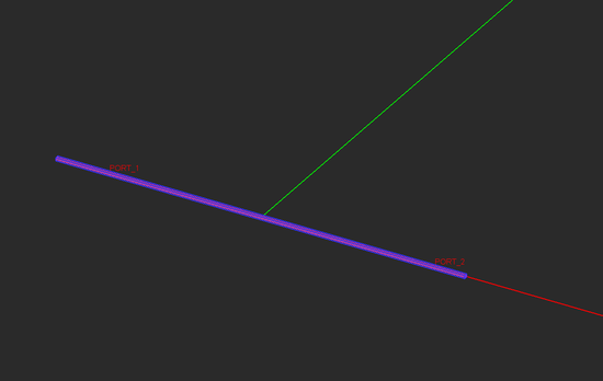
After changing the waveguide dimensions and domain offsets, your waveguide geometry should look like the figure below:
Examining the Sources and Observables
A "Waveguide Port Source" is a distributed source that enforces the dominant modal field of the TE10 propagating mode on a specified plane across the waveguide structure. Waveguide sources are particularly useful when calculating the S-parameters of waveguide circuits. A waveguide source must be associated with a box object whose axis is parallel to one of the three principal axes and has a least one uncapped end. The wizard automatically placed two waveguide port source on the two box objects called "Feed_1" and "Feed_2", which represent the two end sections of the waveguide. The offset parameters of the sources have been set to place them at the center of the two end sections. You can open the property dialog of the waveguide sources "WG_1" and "WG_2" and examine their properties.
The wizard also initiated two field sensors planes, called "SENS_1" and "SENS_2", one Z-directed and the other Y-directed, and both centered at the origin. Define a new third field sensor observable, called "SENS_3", which is X-directed and centered at (0,0,0). Open the property dialog of all three sensors, and change the Plot Type from the default Intensity option to Vector. Also, change the value of Max Size to 0.5 and change the Cone Length Ratio and the Cone Radius Ratio to 0.5 and o.25, respectively. This will generate vector field plots at the end of the FDTD simulation.
Running an FDTD Analysis of the Two-Port Waveguide Structure
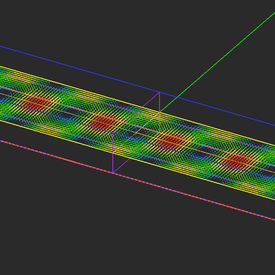
For this project, select the High Precision Mesh Settings from the Mesh Settings dialog. Keep all the default simulation engine settings (power threshold = -30dB and Max. No. Time Steps = 10,000). Run a wideband FDTD Analysis of your waveguide structure. Examine the electric and magnetic field distributions on all the three sensor planes. The electric field distributions on the vertical plane at the center of middle section can easily be identified with a TE10 E-field distribution.
Analyzing the TE10 Modal Fields
The modal fields of the dominant propagating TE10 mode of a rectangular waveguide of dimensions a × b are given by:
[math] E_z = -A \frac{j\omega \mu_0 a}{\pi} \cos \left( \frac{\pi y}{a} \right) e^{-j\beta x} [/math]
[math] H_x = A \sin \left( \frac{\pi y}{a} \right) e^{-j\beta x} [/math]
[math] H_y = A \frac{j\beta a}{\pi} \cos \left( \frac{\pi y}{a} \right) e^{-j\beta x} [/math]
where A is a constant, the waveguide is assumed to be symmetric about the X-axis, and
[math] \beta = \sqrt{k_0^2 - \left( \frac{\pi}{a} \right)^2} [/math]
and ω = 2πf and k0 = ω/c.
The field distributions shown above were computed at the center frequency of fc = 33GHz. At this frequency, the free-space wavelength is λ0 = 9.09mm and k0 = 2πλ0 = 691.15 m-1. Also, kc,TE10 = 2πfc,TE10/c = π/a = 441.23 m-1, and one finds:
[math] \beta = \sqrt{k_0^2 - k_c^2} = 531.98 m^{-1} [/math]
and
[math] \lambda_g= \frac{2\pi}{\beta} = 11.81 mm[/math]
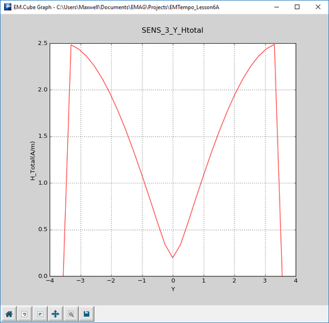
EM.Tempo also generated 2D data files of the total electric and magnetic field distributions along the crosshair axes of the field sensor planes. The position of the crosshair axes can be varied using the coordinates of the field sensor observable. Open the Data Manager and plot the data files "SENS_3_Y_ETotal.DAT" and "SENS_3_Y_HTotal.DAT". From the following figure you can clearly see the cosine variation of the electric field and sine variation of the magnetic field along the Y direction.
Next, plot the data files "SENS_1_X_ETotal.DAT" and "SENS_1_X_HTotal.DAT". These figures show the longitudinal variation of the electric and magnetic fields. Note that the maximum locations of the electric field occur at the minimum locations of the magnetic field and vice versa. This is due to the 90° phase different between the Ez and Hy field components.
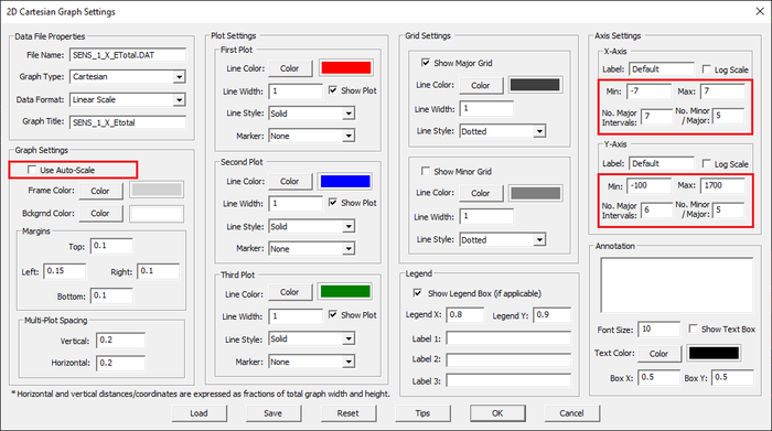
The PyPlot window has a number of controls that let you change the settings of your graph using your mouse. For example, using the Pan/Zoom button ![]() , you can pan the graph with the left mouse button and zoom it in or out with the right mouse button. A combination of the two operations usually gives you an ideal scaling of your graph. As you move the mouse on the graph, you can read the value of the horizontal axis (X) and the corresponding value of the total electric field distribution along the X direction. You can also customize the graphs and change the scale of the graph axes. Click the Graph Settings button and uncheck the Auto box. Enter values -7 and 7 for Min and Max, respectively, for X-Axis and set the No. Major Intervals to 7 in "Axis Settings" panel. Similarly, for Y-Axis enter values -100, 1700, and 6 for Min and Max, and No. Major Intervals respectively.
, you can pan the graph with the left mouse button and zoom it in or out with the right mouse button. A combination of the two operations usually gives you an ideal scaling of your graph. As you move the mouse on the graph, you can read the value of the horizontal axis (X) and the corresponding value of the total electric field distribution along the X direction. You can also customize the graphs and change the scale of the graph axes. Click the Graph Settings button and uncheck the Auto box. Enter values -7 and 7 for Min and Max, respectively, for X-Axis and set the No. Major Intervals to 7 in "Axis Settings" panel. Similarly, for Y-Axis enter values -100, 1700, and 6 for Min and Max, and No. Major Intervals respectively.
The distance between two consecutive field maxima is equivalent to λg/2. First click on the ![]() button to get an enlarged view of middle position of the graph. Move the mouse to the top of one of the field maxima in the graph and read the values on the lower right corner of the status bar, in this case (0.,1464.45). Then move the mouse to the next field maximum and read the values (5.88519,1464.45). You will see Δx = 5.9mm., which is equal to half the calculated guide wavelength.
button to get an enlarged view of middle position of the graph. Move the mouse to the top of one of the field maxima in the graph and read the values on the lower right corner of the status bar, in this case (0.,1464.45). Then move the mouse to the next field maximum and read the values (5.88519,1464.45). You will see Δx = 5.9mm., which is equal to half the calculated guide wavelength.
Alternatively, in the data manager, you can "view" the contents of the data file "SENS_1_X_ETotal.DAT" in the spreadsheet as shown below.
Adding Metallic Irises
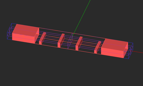
Draw four solid (capped) box objects according to the table below:
| Part | Object Type | Material Type | Dimensions | Coordinates | Rotation Angles | Top End Cap | Bottom End Cap |
|---|---|---|---|---|---|---|---|
| Box1 | Box | PEC | 1mm × 7.12mm × 1.53mm | (-12.41mm, 0, -1.78mm) | (0°, 0°, 0°) | Yes | Yes |
| Box2 | Box | PEC | 1mm × 7.12mm × 1.53mm | (12.41mm, 0, -1.78mm) | (0°, 0°, 0°) | Yes | Yes |
| Box3 | Box | PEC | 1mm × 7.12mm × 2.4mm | (-4.03mm, 0, -1.78mm) | (0°, 0°, 0°) | Yes | Yes |
| Box4 | Box | PEC | 1mm × 7.12mm × 2.4mm | (4.03mm, 0, -1.78mm) | (0°, 0°, 0°) | Yes | Yes |
To draw a box object, click the Box ![]() button of the Object Toolbar or select the menu item Object → Solid → Box.
button of the Object Toolbar or select the menu item Object → Solid → Box.
With the Box tool selected, click on a blank space in the project workspace and drag the mouse to draw the rectangular base of your box object. A property dialog pops up at the lower right corner of your screen. As you drag the mouse, you will see that the X-dimension and Y-dimension of your new object continuously change. When the base reaches the desired size or something close to that, click the mouse. Next, you have to give the right height to your box. Drag the mouse upward until you reach the desired height (Z-dimension). Then, click once more (i.e. drop the mouse). At this time, the drawing of your box is complete. You can always enter values for the dimensions or LCS coordinates at any time.
Your two-port waveguide structure will now look like this:
Running an FDTD Analysis of the Waveguide Filter Structure
Keep the same mesh settings and same FDTD engine settings as the previous part. Run a wideband analysis of your filter structure. After the completion of the simulation, plot the S11 and S21 graphs in PyPlot. The bandpass response of the waveguide filter is clearly visible from the figures below.
