EM.Tempo
Fast Multicore & GPU-Accelerated FDTD Solvers for Simulating the Most Complex Electromagnetic Modeling Problems
Contents
- 1 Product Overview
- 2 EM.Tempo Features at a Glance
- 3 Building the Physical Structure in EM.Tempo
- 4 EM.Tempo's Computational Domain & Boundary Conditions
- 5 EM.Tempo's Excitation Sources
- 6 EM.Tempo's Active & Passive Devices
- 7 EM.Tempo's Observables & Simulation Data Types
- 8 Generating the FDTD Mesh in EM.Tempo
- 9 Running FDTD Simulations in EM.Tempo
- 10 Modeling 3D Periodic Structures in EM.Tempo
Product Overview
EM.Tempo in a Nutshell
EM.Tempo is a powerful electromagnetic simulator for full-wave modeling of 3D radiation, scattering and propagation problems. It features a highly efficient Finite Difference Time Domain (FDTD) simulation engine that has been optimized for speed and memory usage. EM.Tempo brings to your desktop the ultimate in computational power. Its FDTD solver has been parallelized to take full advantage of multi-core processor architectures. With a large variety of geometrical, material and excitation features including open-boundary and periodic structures, you can use EM.Tempo as a general purpose 3D field simulator for most of your electromagnetic modeling needs. EM.Tempo's new advanced simulation capabilities are the key to a thorough understanding of the interaction of electromagnetic waves with complex media such as anisotropic composites, metamaterials or biological environments or with passive and active devices and nonlinear circuits.
EM.Tempo has undergone several evolutionary development cycles since its inception in 2004. The original simulation engine utilized an FDTD formulation based on the uniaxial perfectly matched layer (UPML) boundary termination. Subsequently, a more advanced boundary termination based on the convolutional perfectly matched layer (CPML) was implemented with a far superior performance for all oblique wave incidences in different types of media. EM.Tempo now has the ability to model laterally infinite layered structures using CPML walls that touch material media. A novel formulation of periodic boundary conditions was implemented based on the constant transverse wavenumber method (or direct spectral FDTD). In 2013 we introduced an Open-MP optimized multi-core version of the FDTD engine as well as a hardware-accelerated solver that runs on CUDA-enabled graphical processing unit (GPU) platforms. Both of these fast solvers are now a standard part of the EM.Tempo Pro package.
![]() Click here for an overview of the Basic FDTD Theory.
Click here for an overview of the Basic FDTD Theory.
EM.Tempo as the FDTD Module of EM.Cube
EM.Tempo is a general-purpose EM simulator than can solve most types of electromagnetic modeling problems involving arbitrary geometries and complex material variations in both time and frequency domains. It has also been integrated within the EM.Cube simulation environment as its full-wave "FDTD Module". EM.Tempo shares the visual interface, 3D parametric CAD modeler, data visualization tools, and many more utilities and features collectively known as CubeCAD with all of EM.Cube's other computational modules.
![]() Click here to learn more about EM.Cube Modeling Environment.
Click here to learn more about EM.Cube Modeling Environment.
The Advantages & Limitations of EM.Tempo's FDTD Simulator
A time domain simulation like FDTD offers several advantages over frequency domain simulations. In certain applications, the time domain signature or behavior of a system, e.g. the transient response of a circuit or an antenna, is sought. In other applications, you may need to determine the wideband frequency response of a system. In such cases, using a frequency domain technique, you have to run the simulation engine many times to adequately sample the specified frequency range. In contrast, using the FDTD method requires a single-run simulation. The temporal field data are transformed into the Fourier domain to obtain the wideband frequency response of the simulated system. Among other advantages of the FDTD method are its versatility in handling complex material compositions as well as its superb numerical stability. It is worth noting that unlike most frequency domain methods, the FDTD technique does not involve numerical solution of large ill-conditioned matrix equations that are often very sensitive to the mesh quality.
Like every numerical technique, the FDTD method has disadvantages, too. Adding the fourth dimension, time, to the computations increases the size of the numerical problem significantly. Unfortunately, this translates to both larger memory usage and longer computation times. Note that the field data are generated in both the 3D space and time. EM.Tempo uses a staircase "Yee" mesh to discretize the physical structure. This works perfectly fine for rectangular objects that are oriented along the three principal axes. In the case of highly curved structures or slanted surfaces and lines, however, this may compromise the geometrical fidelity of your structure. EM.Tempo provides a default adaptive FDTD mesher that can capture the fine details of geometric contours, slanted thin layers, surfaces, etc. to arbitrary precision. However, with smaller mesh cells, the stability criterion leads to smaller time steps; hence, longer computation times. Another disadvantage of the FDTD technique compared to naturally open-boundary methods like the method of moments (MoM) is its finite-extent computational domain. This means that to model open boundary problems like radiation or scattering, absorbing boundary conditions are needed to dissipate the incident waves at the walls of the computational domain and prevent them from reflecting back into the domain. The accuracy of the FDTD simulation results depends on the quality of these absorbers and their distance from the actual physical structure. EM.Tempo provides high quality perfectly matched layer (PML) terminations at the boundaries, which can be placed fairly close to your physical structure to reduce the total size of the computational domain.
EM.Tempo Features at a Glance
Physical Structure Definition
- PEC, PMC and dielectric materials and thin wires
- Uniaxial and fully anisotropic materials with four complete constitutive tensors
- Dispersive materials of Debye, Drude and Lorentz types with arbitrary number of poles
- Generalized uniaxial and doubly negative refractive index metamaterials with arbitrary numbers of both electric and magnetic poles
- Two types of gyrotropic materials: ferrites and magnetoplasmas
- PEC, PMC and convolutional perfectly match layer (CPML) boundary conditions
- Doubly periodic structures
Sources, Ports & Devices
- Lumped voltage sources with internal resistance placed on a PEC line or thin wire object with an arbitrary orientation
- Distributed sources with uniform, sinusoidal and edge-singular profiles
- Microstrip, coplanar Waveguide (CPW) and coaxial ports
- Waveguide sources with the dominant TE10 modal profile
- Multi-port and coupled port definitions
- Two types of filamentary current sources: Hertzian short dipole radiators with arbitrary orientation and long wire current sources aligned along one of the principal axes with a uniform, triangular or sinusoidal current distribution profile
- Plane wave excitation with linear and circular polarizations
- Multi-ray excitation capability (ray data imported from EM.Terrano or external files)
- Gaussian beam excitation
- Huygens sources
- Source arrays with weight distribution & phase progression
- Periodic sources with user defined beam scan angles
- Standard excitation waveforms (Gaussian pulse, modulated Gaussian and sinusoidal) for optimal frequency domain computations
- Arbitrary user-defined temporal excitation waveforms using mathematical expressions and Python functions
- Passive lumped devices: R, L, C, series RL and parallel RC and nonlinear diode device
- Active lumped one-port and two-port devices placed on PEC lines aligned along one of the principal axes with arbitrary Netlist definitions
- Active distributed one-port and two-port devices placed under microstrip lines with arbitrary Netlist definitions
Mesh Generation
- Fast generation of Yee grid mesh of solids, surfaces and curves
- Geometry-aware and material-aware adaptive mesh generator with gradual grid transitions
- Fixed-cell uniform mesh generator with three unequal cell dimensions
- Mesh view with three principal grid profilers
- Manual control of mesh parameters and fixed grid points
3D FDTD Simulation
- Wideband full-wave simulation of 3D structures
- Transient analysis with arbitrary user defined excitation waveforms
- Multi-frequency computation of frequency domain quantities in a single FDTD simulation run
- OpenMP-parallelized multi-core and multi-thread FDTD simulation engine
- GPU-accelerated FDTD simulation engine based on NVIDIA CUDA platforms
- Total-field-scattered-field analysis of plane wave and Gaussian beam excitation
- Full-wave analysis of periodic structures with arbitrary plane wave incidence angles using the Direct Spectral FDTD method
- Infinite material half-space Green's functions for calculation of far fields in presence of a lossy ground
- Accelerated computation of S-parameters of resonant structures based on Prony's method of exponential interpolation
- Parametric sweeps of variable object properties or source parameters including frequency and angular sweeps
- Multi-variable and multi-goal optimization of structures
- Automated generation of compact reduced order surrogate models from full-wave simulation data
Data Generation & Visualization
- Near-field intensity (colorgrid), contour and surface plots (vectorial - amplitude & phase)
- Near-field probes for monitoring field components in both time & frequency domains
- Far-field radiation patterns: 3D pattern visualization and 2D polar and Cartesian graphs
- Far-field characteristics such as directivity, beam width, axial ratio, side lobe levels and null parameters, etc.
- Radiation pattern of arbitrary array configurations of the FDTD structure or periodic unit cell
- Bistatic and monostatic radar cross section
- Huygens surface data generation for use in other EM.Cube modules
- Periodic reflection/transmission coefficients and k-β diagrams
- Port characteristics: S/Y/Z parameters, VSWR and Smith chart
- Time and frequency domain port voltages, currents and powers
- Touchstone-style S-parameter text files for direct export to RF.Spice A/D
- Interanl node voltages and currents of Netlist-based one-port and two-port networks
- Computation of electric, magnetic and total energy densities, dissipated power density (Ohmic loss), specific absorption rate (SAR) density and complex Poynting vector on field sensor planes
- Animation of temporal evolution of fields
- Custom output parameters defined as mathematical expressions or Python functions of standard outputs
Building the Physical Structure in EM.Tempo
Material Variety in EM.Tempo
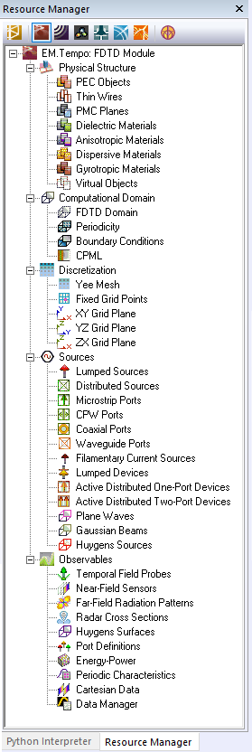
Your physical structure in EM.Tempo can be made up of several geometric objects with different material compositions. In other words, the geometric objects you draw or import from external files are grouped together based on a common material composition. EM.Tempo's material types are divided into seven categories:
| Icon | Material Type | Applications | Geometric Object Types Allowed |
|---|---|---|---|
| |
Perfect Electric Conductor (PEC) | Modeling perfect metals | Solid, surface and curve objects |
| |
Thin Wire | Modeling wire radiators | Lines parallel to one of the three principal axes |
| |
Perfect Magnetic Conductor (PMC) | Modeling perfect magnetic sheets | Rectangle strips parallel to one of the three principal planes |
| |
Dielectric Material | Modeling any homogeneous material | Solid objects |
| |
Anisotropic Material | Modeling unaxial or generalized anisotriopic materials | Solid objects |
| |
Dispersive Material | Modeling Debye, Drude and Lorentz materials and generalized metamaterials | Solid objects |
| |
Gyrotropic Material | Modeling ferrites and magnetoplasmas | Solid objects |
| |
Virtual Object | Used for representing non-physical items | All types of objects |
Click on each category to learn more details about it in the Glossary of EM.Cube's Materials, Sources, Devices & Other Physical Object Types.
Organizing the Physical Structure by Material Groups
EM.Tempo groups your geometric objects in the project workspace based on their material type. All the objects belonging to the same material group share the same color and same material properties. Under each material node in the navigation tree, you can create new material groups of the same type but with different properties such as color, texture, or electric and magnetic constitutive parameters.
Once a new material node has been created on the navigation tree, it becomes the "Active" material group of the project workspace, which is always listed in bold letters. When you draw a new geometric object such as a box or a sphere, its name is added under the currently active material type. There is only one material group that is active at any time. Any material can be made active by right clicking on its name in the navigation tree and selecting the Activate item of the contextual menu. It is recommended that you first create material groups, and then draw new objects under the active material group. However, if you start a new EM.Tempo project from scratch, and start drawing a new object without having previously defined any material groups, a new default PEC group is created and added to the navigation tree to hold your new object.
| |
You can import external objects only to CubeCAD. You can then move the imported objects form CubeCAD to EM.Tempo. |
![]() Click here to access the Glossary of EM.Cube's Materials, Sources, Devices & Other Physical Object Types.
Click here to access the Glossary of EM.Cube's Materials, Sources, Devices & Other Physical Object Types.
Material Hierarchy in EM.Tempo
EM.Tempo allows overlapping objects although it is generally recommended that object overlaps be avoided in favor of clearly defined geometries and object boundaries. If two or more objects of the same material type and group overlap, they are merged using the Boolean union operation during the mesh generation process. If two overlapping objects belong to two different material categories, then the material properties of the FDTD cells in the overlap region will follow the EM.Tempo's material hierarchy rule. In that case, the overlap area cells will always be regarded as having the material type of the higher priority. According to this rule, the material types are ordered from the highest priority to the lowest in the following manner:
- PEC
- PMC
- Dispersive
- Gyrotropic
- General Anisotropic
- Uniaxial Anisotropic
- Dielectric
If planned carefully, taking advantage of EM.Tempo's material hierarchy rule would make the construction of complex objects easier. For example, a dielectric coated metallic cylinder can be modeled by two concentric cylinders: an inner PEC of smaller radius and an outer dielectric of larger radius as shown in the illustration below. The portion of the dielectric cylinder that overlaps the inner PEC cylinder is ignored by the FDTD engine because the PEC cylinder takes precedence over the dielectric in the material hierarchy. Alternatively, you can model the same structure by an inner solid PEC cylinder enclosed by an outer hollow pipe-shaped dielectric cylinder.
Moving Objects Among Different Material Groups or EM.Cube Modules
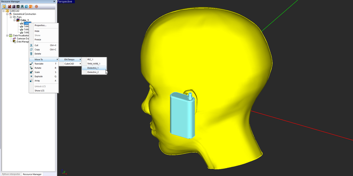
You can move any geometric object or a selection of objects from one material group to another. You can also transfer objects among EM.Cube's different modules. For example, you often need to move imported CAD models from CubeCAD to EM.Tempo. To transfer objects, first select them in the project workspace or select their names in the navigation tree. Then right-click on them and select Move To → Module Name → Object Group from the contextual menu. For example, if you want to move a selected object to a material group called "Dielectric_1" in EM.Tempo, then you have to select the menu item Move To → EM.Tempo → Dielectric_1 as shown in the figure below. Note that you can transfer several objects altogether using the keyboards's Ctrl or Shift keys to make multiple selections.
EM.Tempo's Computational Domain & Boundary Conditions
The FDTD Solution Domain
The FDTD method requires a finite-extent solution domain. This is rather straightforward for shielded structures, where a typical PEC enclosure box defines the computational domain. For open-boundary structures like antennas and scatterers, the computational domain must be truncated using appropriate termination boundary conditions. The objective of termination boundary conditions is to eliminate the reflections from the walls of the domain box back to the computational domain.
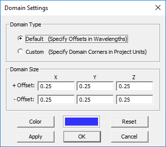
In EM.Tempo, you can define two types of domain box. A Default-type domain is a box that is placed at a specified offset distance from the largest extents of your physical structure (global bounding box). The offset is specified in free-space wavelengths. A Custom-type domain, on the other hand, is defined as a fixed-size and fixed-location box in the World Coordinate System (WCS). In this case, you have to specify the coordinates of the lower left front corner (Corner 1) and upper right back corner (Corner 2) of the domain box.
When you start a new project in EM.Tempo, a default-type domain is automatically created with a default offset value set equal to a quarter free-space wavelength (0.25λ0). As soon as you draw your first object, a blue domain box shows up in the project workspace and encloses your object. As you add more objects and increase the overall size of your structure, the domain box grows accordingly to encompass your entire physical structure. When you delete objects from the project workspace, the domain box also shrinks accordingly.
Changing the Domain Settings
To set the solution domain of your FDTD project, follow these steps:
- Click the Domain
 button of the Simulate Toolbar or select the menu item Simulate → Computational Domain → Domain Settings... or right click on the FDTD Domain item of the Navigation Tree and select Domain Settings... from the contextual menu, or use the keyboard shortcut Ctrl+A. The Domain Settings Dialog opens up, showing the current domain type selection.
- Select one of the two options for Domain Type: Default or Custom.
- If you select the "Default" domain type, the domain box is defined in terms of the offsets along the X, Y and Z directions from the largest extents of your physical structure. Select one of the two options for Offset Units: Grid and Wavelength. In the section titled "Domain Size", enter the amount of domain extension beyond the largest extents of the structure along the ±X, ±Y and ±Z directions. Note that in the case of a default-type domain box, the offset values based on your current project settings (frequency and units).
- When the Wavelength option is selected for Offset Units, additional free space is added around the structure by the specified ±X, ±Y and ±Z offsets in free space wavelengths. Note that the free space wavelength for this purpose is calculated at the center frequency of the project. The default value of the offset in this case is a quarter free space wavelength. Note that with this option, the number of the additional cells and their cell size is not fixed; they vary from structure to structure.
- When the Grid option is selected for Offset Units, the six offset values represent the number of additional free-space mesh cells that are placed in each direction beyond the largest bounding box around the physical structure. The default value of the offset in this case is eight grid cells along the ±X, ±Y and ±Z directions.
- If you select the "Custom" domain type instead, you need to enter values for the coordinates of the lower-left-front corner, Corner 1, and the upper-right-back corner, Corner 2, of the domain box.
- After you change values or settings, click the Apply button to make the changes effective. To recover the default values, click the Defaults button of the dialog. Click OK to save the settings and close the dialog.
By default, the domain box is shown as a wireframe box with blue lines. You can change the color of the domain box or hide it.
![]() Click here to learn more about Domain Settings.
Click here to learn more about Domain Settings.
Settings the Domain Boundary Conditions
EM.Tempo supports four types of domain boundary conditions: PEC, PMC, Convolutional Perfectly Matched Layers (CPML) and Periodic Boundary Conditions (PBC). By default, all the six sides of the computational domain box are set to CPML, representing a completely open-boundary structure. Different boundary conditions can be assigned to each of the six walls of the domain box. The periodic boundary conditions are special ones that are assigned through EM.Tempo's Periodicity Dialog and will be discussed later under modeling of periodic structures. The current release of EM.Cube allows periodic boundary conditions only on the side walls of the computational domain, and not on the top or bottom walls.
To define the boundary conditions of the solution domain, follow these steps:
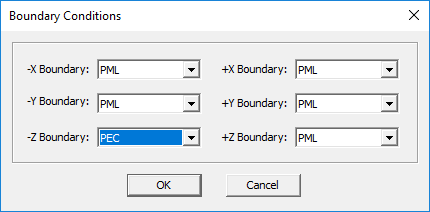
- Select the menu item Simulate → Computational Domain → Boundary Conditions or right click on the Boundary Conditions item in the Computational Domain section of the Navigation Tree and select Boundary Conditions... from the contextual menu. The Boundary Conditions Dialog opens.
- You need to assign the type of boundary condition on each of the six domain boundaries: ±X, ±Y and ±Z. For each face, choose one of the three options available: PEC, PMC or PML.
The PEC and PMC boundary conditions are the most straightforward to set up and use. Assigning the PEC boundary to one of the bounding walls of the solution domain simply forces the tangential component of the electric field to vanish at all points along that wall. Similarly, assigning the PMC boundary to one of the bounding walls of the solution domain forces the tangential component of the magnetic field to vanish at all points along that wall. For planar structures with a conductor-backed substrate, you can use the PEC boundary condition to designate the bottom of the substrate (the -Z Domain Wall) as a PEC ground. For shielded waveguide structures, you can designate all the lateral walls as PEC. Similarly to model shielded cavity resonators, you designate all the six walls as PEC.
Advanced CPML Setup
In open-boundary electromagnetic modeling problems, you need a boundary condition that simply absorbs all the incoming radiation. For problems of this nature, an absorbing boundary condition (ABC) is often chosen that effectively minimizes wave reflections at the boundary. EM.Tempo uses Convolutional Perfectly Matched Layers (CPML) for absorbing boundary conditions. Usually two or more ABC layers must be placed at the boundaries of the physical structure to maximize wave absorption. The boundary CPML cells in the project workspace are not visible to the user. But, in effect, multiple rows of CPML cells are placed on the exterior side of each face of the visible domain box.
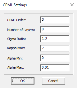
You can set the number of CPML layers as well as their order. This is done through the CPML Settings Dialog, which can be accessed by right clicking on the CPML item in the Computational Domain section of the navigation tree and selecting CPML Settings... from the contextual menu. By default, eight CPML layers of the third order are placed outside the FDTD problem domain. It is recommended that you always try a four-layer CPML first to assess the computational efficiency. The number of CPML layers may be increased if a very low reflection is required (<-40dB).
![]() Click here to learn more about the theory of Perfectly Matched Layer Termination.
Click here to learn more about the theory of Perfectly Matched Layer Termination.
Using CPML to Model Structures of Infinite Extents
You can use EM.Tempo to model planar structures of infinite extents. A planar substrate usually consists of one or more dielectric layers, possibly with a PEC ground plane at its bottom. To model a laterally infinite dielectric substrate, you must assign a PML boundary condition to the four lateral sides of the domain box and set the lateral domain offset values along the ±X and ±Y directions all equal to zero. If the planar structure ends in an infinite dielectric half-space from the bottom, you must assign a PML boundary condition to the bottom side of the domain box and set the -Z offset equal to zero. This leaves only the +Z offset with a nonzero value.
When a domain boundary wall is designated as CPML and its has a zero domain offset, meaning it touches a material block, the CPML cells outside the domain wall are reflected back inside the computational domain. In other words, the effective number of CPML layers will be twice the one specified in the CPML Settings dialog. This will effectively extend the material block infinitely beyond the boundary wall and will create an open boundary effect in the specified direction. It goes without saying that only "substrate" objects are supposed to touch the boundary walls in such a scenario. Because of the rolled-back CPML cells inside the domain, it is very important to make sure that other finite-sized parts and objects stay clear from the domain walls as well as from the invisible "interior" CPML cells.
EM.Tempo's Excitation Sources
Source Variety in EM.Tempo
Before you can run an FDTD simulation, you have to define a source to excite your project’s physical structure. EM.Tempo offers a variety of excitation mechanisms for your physical structure depending on your particular type of modeling problem or application:
| Icon | Source Type | Applications | Host Object | Spatial Domain | Restrictions / Additional Requirements |
|---|---|---|---|---|---|
| |
Lumped Source | General-purpose point voltage source | PEC or thin wire line parallel to a principal axis | A single point | None |
| |
Distributed Source | General-purpose distributed planar source with a uniform, edge-singular or sinusoidal impressed field profile | Virtual rectangle strip parallel to a principal plane | A rectangular area | None |
| |
Microstrip Port Source | Used for S-parameter computations in microstrip-type structures | PEC rectangle strip parallel to a principal plane | A vertical rectangular area underneath the host strip | Requires a PEC ground plane strip underneath the host strip |
| |
Coplanar Waveguide (CPW) Port Source | Used for S-parameter computations in CPW-type structures | PEC rectangle strip parallel to a principal plane | Two parallel horizontal rectangular areas attached to the opposite lateral edges the host center strip | Requires two parallel PEC ground strips on the two sides of the host center strip |
| |
Coaxial Port Source | Used for S-parameter computations in coaxial-type structures | PEC Cylinder oriented along a principal axis | A circular ring area enveloping the host inner conductor cylinder | Requires a concentric hollow outer conductor cylinder |
| |
Waveguide Port Source | Used for S-parameter computations in waveguide structures | Hollow PEC box oriented along a principal axis | A rectangular area at the cross section of the host hollow box | The host box object can have one capped end at most. |
| |
Filamentary Current Source | General-purpose wire current source of two types: Hertzian short dipole radiator and long wire current source with a uniform, triangular or sinusoidal current distribution profile | None (stand-alone source) | A line | Hertzian short dipole radiators can have an arbitrary orientation, but long wire current sources must be aligned along one of the principal axes |
| |
Plane Wave Source | Used for modeling electromagnetic scattering & computation of reflection/transmission characteristics of periodic surfaces | None (stand-alone source) | Surface of a cube enclosing the physical structure | None |
| |
Gaussian Beam Source | Used for modeling focused beams | None (stand-alone source) | Surface of a cube enclosing the physical structure | None |
| |
Huygens Source | Used for modeling equivalent sources imported from other EM.Cube modules | None (stand-alone source) | Surface of a cube | Imported from a Huygens surface data file |
Click on each category to learn more details about each source type and how to define one.
![]() More information about all the source types can be found in the Glossary of EM.Cube's Materials, Sources, Devices & Other Physical Object Types.
More information about all the source types can be found in the Glossary of EM.Cube's Materials, Sources, Devices & Other Physical Object Types.
In the most general sense, one can consider two fundamental types of excitation sources for an FDTD simulation: a lumped source and a distributed source. A lumped sources is localized at a single mesh point in the computational domain, while a distributed source is spread over several mesh cells. Among the source types of the above list, the microstrip port, CPW port, coaxial port, waveguide port, plane wave and Gaussian beam sources are indeed special cases of a distributed source for specific applications.
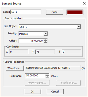
A lumped source is the most commonly used way of exciting a structure in EM.Tempo. A lumped source is a voltage source with a series internal resistor that must be placed on a PEC or thin wire line object that is parallel to one of the three principal axes. A lumped source is displayed as a small red arrow on the host line. Lumped sources are typically used to define ports and compute the port characteristics like S/Y/Z parameters. Using simple lumped sources, you can simulate a variety of transmission line structures including filters, couplers or antenna feeds. This approach may become less accurate at higher frequencies when the details of the feed structure become important and can no longer be modeled with highly localized lumped ports. In such cases, it is recommended to use “Distributed Sources”, which utilize accurate modal field distributions at the ports for calculation of the incident and reflected waves. Waveguide source is used to excite the dominant TE10 mode of a hollow rectangular waveguide. Other special types of distributed sources are microstrip port, CPW port and coaxial ports that can be used effectively to excite their respective transmission line structures.
When you create an array of an object type that can host one of the above source types, you can also associate a source array with that array object.
![]() Click here to learn more about Modeling Finite-Sized Source Arrays.
Click here to learn more about Modeling Finite-Sized Source Arrays.
A plane wave source is a popular excitation method that is used for calculation of the radar cross section of targets or reflection and transmission characteristics of periodic surfaces. A Gaussian beam source is another source type that is highly localized as opposed to the uniform plane wave. For both plane wave and Gaussian beam sources,[EM.Tempo requires a finite incidence surface to calculate the excitation. When you create either of these sources, a plane wave box or a Gaussian beam box is created as part of their definition. A trident symbol on the box shows the propagation vector as well as the E-field and H-field polarization vectors. The time domain plane wave or Gaussian beam excitation is calculated on the surface of this box and injected into the computational domain. The plane wave box is displayed in the project workspace as a purple wireframe box enclosing the structure, while the Gaussian beam box appears as a green wireframe box. Both boxes have an initial default size with an offset of 0.2λ0 from the largest bounding box enclosing your entire physical structure. In both source dialogs, the radio button Size: Default is selected by default. The radio button Size: Custom allows you to set the excitation box manually. The values for the coordinates of Corner 1 and Corner 2 can now be changed. Corner 1 is the front lower left corner and Corner 2 is the rear upper right corner of the box. The corner coordinates are defined in the world coordinate system (WCS).
Simulating a Multiport Structure in EM.Tempo
Ports are used to order and index sources for circuit parameter calculations like S/Y/Z parameters. In EM.Tempo, you can define ports at the location of the following types of sources:
- Lumped sources
- Distributed sources
- Microstrip port sources
- CPW port sources
- Coaxial port sources
- Waveguide port sources
Every time you create a new source with one of the above types, the program asks if you want to initiate a new port and associate it with the newly created source. If the physical structure of your project workspace has N sources, then N default ports are defined, with one port assigned to each source according to their order in the navigation tree. You can define any number of ports equal to or less than the total number of sources in your project.
If your physical structure has two or more sources, but you have not defined any ports, all the sources will excite the structure simultaneously during the simulation. However, when you assign N ports to the sources, then you have a multiport structure that is characterized by an N×N scattering matrix, an N×N impedance matrix, and an N×N admittance matrix. To calculate these matrices, EM.Tempo uses a binary excitation scheme in conjunction with the principle of linear superposition. In this binary scheme, the structure is analyzed a total of N times. Each time one of the N port-assigned sources is excited, and all the other port-assigned sources are turned off. In other words, the FDTD solver runs a "port sweep" internally. When the jth port is excited, all the Sij parameters are calculated together based on the following definition:
- [math] S_{ij} = \sqrt{\frac{Re(Z_i)}{Re(Z_j)}} \cdot \frac{V_j - Z_j^*I_j}{V_i+Z_i I_i} [/math]
where Vi is the voltage across Port i, Ii is the current flowing into Port i and Zi is the characteristic impedance of Port i. The sweep loop then moves to the next port until all ports have been excited.
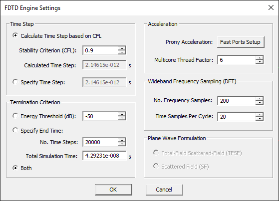
In summary, to analyze an N-port structure, EM.Tempo runs N separate FDTD time marching loops. The S/Z/Y parameters are frequency-domain quantities. The port voltages and currents are Fourier-transformed to the frequency domain over the frequency range [fc-bw/2, fc+bw/2], where fc is the center frequency and bw is the bandwidth of your project. You can reduce the frequency range of the Fourier transform by settings new values for Start and End frequencies in the "Port Definition" dialog as long as these are within the range [fc-bw/2, fc+bw/2]. By default, 200 frequency samples are taken over the specified frequency range. This number can be modified from the FDTD simulation engine settings dialog.
![]() Click here to learn more about the Port Definition Observable.
Click here to learn more about the Port Definition Observable.
![]() Click here to learn more about Modeling Coupled Sources & Ports.
Click here to learn more about Modeling Coupled Sources & Ports.
Excitation Waveform & Frequency Domain Computations
When an FDTD simulation starts, your project's source starts pumping energy into the computational domain at t > 0. Maxwell's equations are solved in all cells at every time step until the solution converges, or the maximum number of time steps is reached. A physical source has a zero value at t = 0, but it rises from zero at t > 0 according to a specified waveform. EM.Tempo currently offers four types of temporal waveform:
- Sinusoidal
- Gaussian Pulse
- Modulated Gaussian Pulse
- Arbitrary User-Defined Function
A sinusoidal waveform is single-tone and periodic. Its spectrum is concentrated around a single frequency, which is equal to your project's center frequency. A Gaussian pulse decays exponentially as t → ∞, but it has a lowpass frequency spectrum which is concentrated around f = 0. A modulated Gaussian pulse decays exponentially as t → ∞, and it has a bandpass frequency spectrum concentrated around your project's center frequency. For most practical problems, a modulated Gaussian pulse waveform with EM.Tempo's default parameters provides an adequate performance.
The accuracy of the FDTD simulation results depends on the right choice of temporal waveform. EM.Tempo's default waveform choice is a modulated Gaussian pulse. At the end of an FDTD simulation, the time domain field data are transformed into the frequency domain at your specified frequency or bandwidth to produce the desired observables.
| |
All of EM.Tempo's excitation sources have a default modulated Gaussian pulse waveform unless you change them. |
![]() Click here to learn more about EM.Tempo's Standard & Custom Waveforms and Discrete Fourier Transforms.
Click here to learn more about EM.Tempo's Standard & Custom Waveforms and Discrete Fourier Transforms.
Defining Custom Waveforms in EM.Tempo
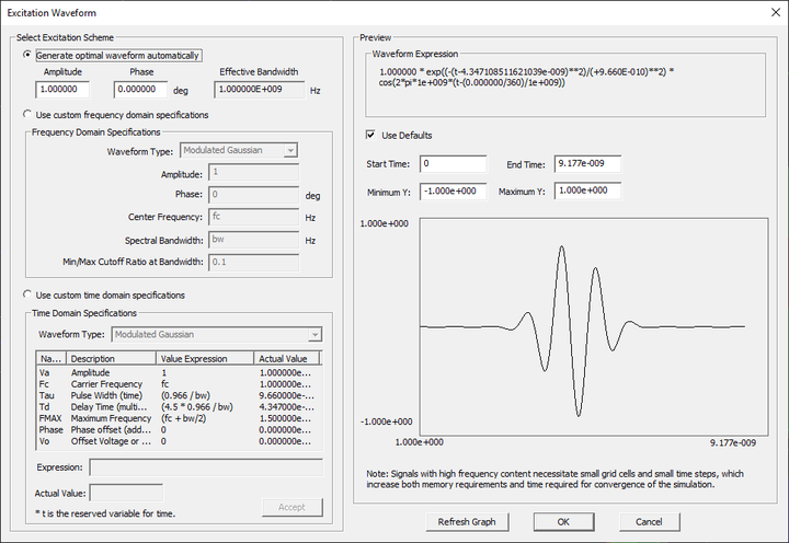
In some time-domain applications, you may want to simulate the propagation of a certain kind of waveform in a circuit or structure. In addition to the default waveforms, EM.Tempo allows you to define custom waveforms by either time or frequency specifications for each individual source in your project. If you open up the property dialog of any source type in EM.Tempo, you will see an Excitation Waveform... button located in the "Source Properties" section of the dialog. Clicking this button opens up EM.Tempo's Excitation Waveform dialog. From this dialog, you can override EM.Tempo's default waveform and customize your own temporal waveform. The Excitation Waveform dialog offers three different options for defining the waveform:
- Automatically Generate Optimal Waveform
- Use Custom Frequency Domain Specifications
- Use Custom Time Domain Specifications
The first option, which is also the default option, constructs an optimal modulated Gaussian pulse waveform based on your project's specified center frequency and bandwidth. This optimal waveform guarantees the most accurate frequency domain computations for your simulation. The second option gives you a choice of the three standard waveforms and lets you define their waveform parameters in terms of frequency domain characteristics like center frequency and bandwidth and spectral contents. The third option lets you define a completely arbitrary temporal waveform for your source.
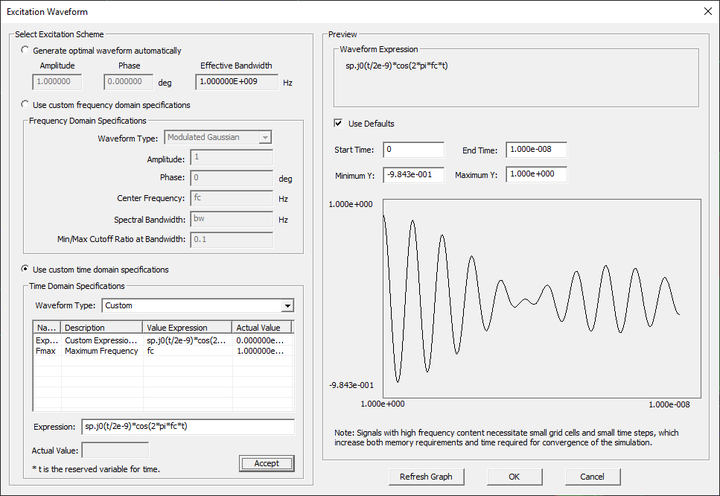
Select the third option of waveform definition and then choose the Custom option from the Waveform Type dropdown list. Enter a mathematical expression for your custom waveform a function of the time variable "T" or "t" in the box labeled Expression. You can use arithmetic operations, standard and library functions as well as user-defined Python functions.
![]() Click here to learn more about Creating Custom Python Functions.
Click here to learn more about Creating Custom Python Functions.
When you define a custom waveform in the Excitation Waveform dialog, make sure to click the Accept button of the dialog to make your changes effective. A graph of your custom waveform is plotted in the right panel of the dialog for your review. It is important to keep in mind that typical time scales in the FDTD simulation of RF structures are on the order of nanosecond or smaller. Using the variable "fc" in the expression of your waveform definition usually takes care of this required scaling. Otherwise, you need to use scaling factors like 1e-9 explicitly in your expression. For example, in the figure below, we have defined a modulated Bessel waveform in the form of "sp.j0(t/2e-9)*sin(2*pi*fc*t)", where sp.j0(x) denotes the zeroth-order Bessel function of the first kind burrowed from Python's special functions module.
![]() Click here to learn more about Python's Standard & Advanced Mathematical Functions.
Click here to learn more about Python's Standard & Advanced Mathematical Functions.
| |
If you define a custom excitation waveform for your source, none of the standard frequency domain output data and parameters will be computed at the end of your FDTD simulation. |
EM.Tempo's Active & Passive Devices
Defining Lumped Devices
In EM.Tempo, you can define eigth types of lumped devices:
- Resistor
- Inductor
- Capacitor
- Series RL Device
- Parallel RC Device
- Nonlinear Diode
- Active Lumped One-Port Device
- Active Lumped Two-Port Device
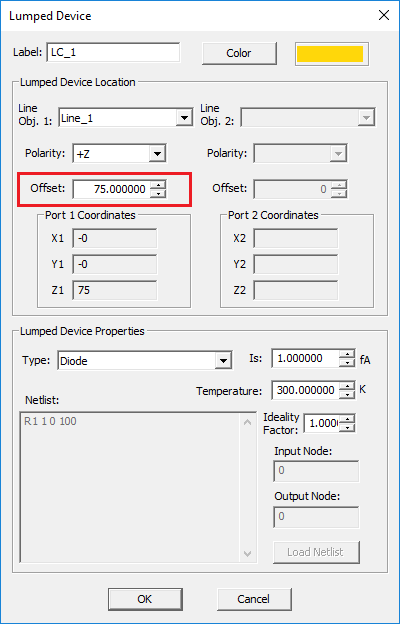
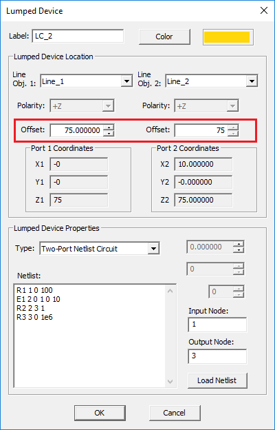
Lumped devices are connected between two adjacent FDTD mesh nodes. Although lumped devices are not sources and the passive types do not excite a structure, their properties are similar to lumped sources. That is why they are listed under the Sources section of the navigation tree. A lumped device has to be associated with a PEC line object that is parallel to one of the three principal axes. Similar to lumped sources, lumped devices have an Offset parameter that is equal to the distance between their location on the host line and its start point.
A lumped device is characterized by a v-i equation of the form:
- [math]i(t) = L \{ v(t) \} [/math]
where V(t) is the voltage across the device, i(t) is the current flowing through it and L is an operator function, which may involve differential or integral operators. Lumped devices are incorporated into the FDTD grid across two adjacent nodes in a similar manner to lumped sources. At the location of a lumped device, the FDTD solver enforces the device's governing equation by relating the device voltage and current to the electric and magnetic field components and updating the fields accordingly at every time step.
![]() Click here for a general discussion of Linear & Nonlinear Passive & Active Devices.
Click here for a general discussion of Linear & Nonlinear Passive & Active Devices.
Defining Active Distributed Multiport Networks
EM.Tempo also provides two types of active distributed multiport network devices:
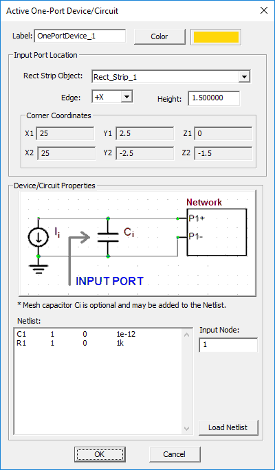
Unlike the active lumped devices, these devices are rather distributed and their behavior is similar to a microstrip port source. In other words, the active distributed one-port device requires a rectangle strip object as a host, while the active distributed two-port device requires two rectangle strip objects for its definition. You can choose one of the edges of the strip object for establishing the circuit port. In the case of a two-port device, you need two parallel and end-to-end aligned strip objects.
The circuit behavior of these devices is defined by a Netlist file. Their property dialog provides a text editor for simply writing the Netlist description of the device. You can also import an existing external Netlist file with a ".CIR" or ".TXT" file extension using the button labeled Load Netlist..
| |
RF.Spice A/D can generate a Netlist file corresponding to an existing circuit project, which can then be saved to a text file with a ".TXT" file extension. |
A Note on Using Active Devices
When your physical structure contains an active device, EM.Tempo performs an EM-circuit co-simulation that involves both the full-wave FDTD EM solver and the SPICE circuit solver. In a global self-consistent co-simulation, at each time step of the FDTD time marching loop, the electric and magnetic fields at the location of the device ports are used to compute the port voltages and currents. These quantities are then used in the SPCIE circuit solver to update all the voltages and currents at the internal nodes of the active device. The updated port voltages and currents are finally used to update the electric and magnetic fields in the physical mesh cells and the time marching loop proceeds to the next time step.
EM.Tempo can handle several active one-ports and two-ports simultaneously. In that case, all the devices are automatically compiled into a single Netlist that serves as the input of the SPICE solver. The individual internal nodes of each device need to be renamed for the global Netlist. Besides the main circuit, the Netlist of each device may contain several "subcircuits". Note that the subcircuit nodes are not re-indexed for the global Netlist as is expected.
| |
If you want to use a B-type nonlinear dependent source in the Netlist definition of an active one-port or two-port, it must be contained in a subcircuit definition rather than in the main circuit. |
The figure below shows the geometry of a two-port amplifier device with microstrip input and output transmission lines. The Netlist of the two-port device is given below:
C1 1 0 1p
R1 1 0 50
E1 2 0 1 0 20
RS 2 3 10
R2 3 0 50
C2 3 0 1p
In this case, a linear voltage-controlled voltage source (E1) with a voltage gain of 20 has been used. The input and output nodes are 1 and 3, respectively.
The same Netlist can be written using a B-type nonlinear dependent source as follows:
C1 1 0 1p
X1 1 0 2 0 amp_dev
.subckt amp_dev 1 2 3 4
R1 1 2 50
B1 3 4 v = 20*v(1,2)
.ends
RS 2 3 10
R2 3 0 50
C2 3 0 1p
| |
You can use active one-ports to define custom voltage or current sources for your entire physical structure rather than using one of the physical excitation source types of the navigation tree. |
EM.Tempo's Observables & Simulation Data Types
Understanding the FDTD Observable Types
EM.Tempo's FDTD simulation engine calculates all the six electric and magnetic field components (Ex, Ey, Ez, Hx, Hy and Hz) at every mesh grid node at all time steps from t = 0 until the end of the time marching loop. However, in order to save memory usage, the engine discards the temporal field data from each time step to the next. Storage, manipulation and visualization of 3D data can become overwhelming for complex structures and larger computational domains. Furthermore, calculation of some field characteristics such as radiation patterns or radar cross section (RCS) can be sizable, time-consuming, post-processing tasks. That is why EM.Tempo asks you to define project observables to instruct what types of output data you want in each simulation process.
EM.Tempo offers the following types of output simulation data:
| Icon | Simulation Data Type | Associated Observable Type | Applications | Restrictions |
|---|---|---|---|---|
| |
Temporal Waveforms | Temporal Field Probe | Computing electric and magnetic field components at a fixed location in the time domain | None |
| |
Point Fields | Temporal Field Probe | Computing the amplitude and phase of electric and magnetic field components at a fixed location in the frequency domain | None |
| |
Near-Field Distribution Maps | Near-Field Sensor | Computing the amplitude and phase of electric and magnetic field components on a planar cross section of the computational domain in the frequency domain | None |
| |
Time-Domain Near-Field Animation | Near-Field Sensor | Computing either total electric or total magnetic field distribution on a planar cross section of the computational domain in the time domain | The field maps are generated at certain specified time intervals |
| |
Far-Field Radiation Patterns | Far-Field Radiation Pattern | Computing the 3D radiation pattern in spherical coordinates | Requires one of these source types: lumped, distributed, microstrip, CPW, coaxial or waveguide port |
| |
Far-Field Radiation Characteristics | Far-Field Radiation Pattern | Computing additional radiation characteristics such as directivity, axial ratio, side lobe levels, etc. | Requires one of these source types: lumped, distributed, microstrip, CPW, coaxial or waveguide port |
| |
Far-Field Scattering Patterns | Far-Field Radiation Pattern | Computing the 3D scattering pattern in spherical coordinates | Requires a plane wave or Gaussian beam source |
| |
Radar Cross Section | RCS | Computing the bistatic and monostatic RCS of a target | Requires a plane wave source |
| |
Polarimetric Scattering Matrix Data | RCS | Computing the scattering matrix of a target for various plane wave source incident angles | Requires a plane wave source |
| |
Port Characteristics | Port Definition | Computing the S/Y/Z parameters and voltage standing wave ratio (VSWR) | Requires one of these source types: lumped, distributed, microstrip, CPW, coaxial or waveguide port |
| |
Port Voltages, Currents & Powers | Port Definition | Computing the port voltages, port currents and total port powers in both time and frequency domains | Requires one of these source types: lumped, distributed, microstrip, CPW, coaxial or waveguide port |
| |
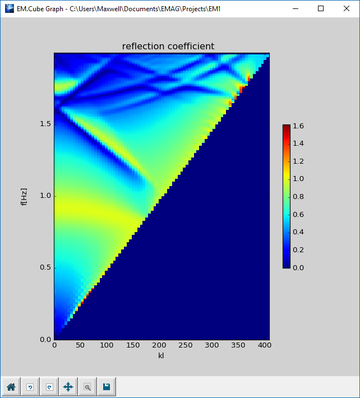
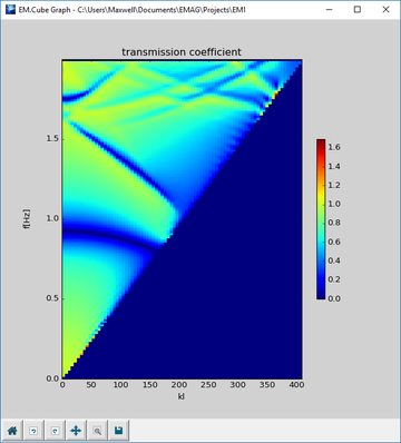
Periodic Reflection & Transmission Coefficients | Periodic Characteristics (No observable definition required) | Computing the reflection and transmission coefficients of a periodic surface | Requires a plane wave source and periodic boundary conditions |
| |
Electric and Magnetic Energy | Energy-Power | Computing the electric, magnetic and total energy inside the entire computational domain in the time domain | None |
| |
Dissipated Power | Energy-Power | Computing the total dissipated power inside the entire computational domain in the time domain | None |
| |
Electric and Magnetic Energy Density | Energy-Power | Computing the electric, magnetic and total energy density on a field sensor plane in the frequency domain | Requires at least one field sensor observable |
| |
Dissipated Power (Ohmic Loss) Density and Specific Absorption Rate (SAR) Density | Energy-Power | Computing the dissipated power density and SAR density on a field sensor plane in the frequency domain | Requires at least one field sensor observable |
| |
Poynting Vector | Energy-Power | Computing the complex Poynting vector on a field sensor plane in the frequency domain | Requires at least one field sensor observable |
| |
Equivalent Electric and Magnetic Surface Currents | Huygens Surface | Collecting tangential field data on a box to be used later as a Huygens source in other EM.Cube modules | None |
| |
Generic 3D Cartesian Spatial Data | 3D Cartesian Data | Visualizing the contents of generic 3D Cartesian spatial data files overlaid on the project workspace | Requires import of an existing ".CAR" data file |
Click on each category to learn more details about it in the Glossary of EM.Cube's Simulation Observables & Graph Types.
Of EM.Tempo's frequency domain observables, the near fields, far fields and all of their associated parameters like directivity, RCS, etc., are calculated at a certain single frequency that is specified as part of the definition of the observable. To compute those frequency domain data at several frequencies, you need to define multiple observables, one for each frequency. On the other hand, port characteristics like S/Y/Z parameters and VSWR are calculated over the entire specified bandwidth of your project. Of EM.Tempo's source types, lumped sources, waveguide sources and distributed sources let you define one or more ports for your physical structure and compute its port characteristics. One of EM.Tempo's real advantages over frequency-domain solvers is its ability of generate wideband S/Z/Y parameter data in a single simulation run.
Examining the Near Fields in Time and Frequency Domains
EM.Tempo's FDTD time marching loop computes all the six electric and magnetic field components at every Yee cell of your structure's mesh at every time step. This amounts to a formidable amount of data that is computationally very inefficient to store. Instead, you can instruct EM.Tempo to save a small potion of these data for visualization and plotting purposes. Using a Field Probe at a specified point, you can record the a time-domain field component over the entire FDTD loop. The time-domain results are also transformed to the frequency domain within the specified bandwidth using a discrete Fourier transform (DFT).
In EM.Tempo, you can visualize the near fields at a specific frequency in a specific plane of the computational domain. To do so, you need to define a Field Sensor observable. EM.Tempo's field sensor defines a plane across the entire computational domain parallel to one of the three principal planes. The magnitude and phase of all the six components of the electric and magnetic fields on the mesh grid points on the sensor plane are computed and displayed.
Computing Far-Field Characteristics in FDTD
Far fields are the asymptotic form the fields when r → ∞ or k0r >> 1. Under these assumptions, the fields propagate outward as transverse electromagnetic (TEM) waves:
[math] \mathbf{H^{ff}(r)} = \frac{1}{\eta_0} \mathbf{ \hat{k} \times E^{ff}(r)} [/math]
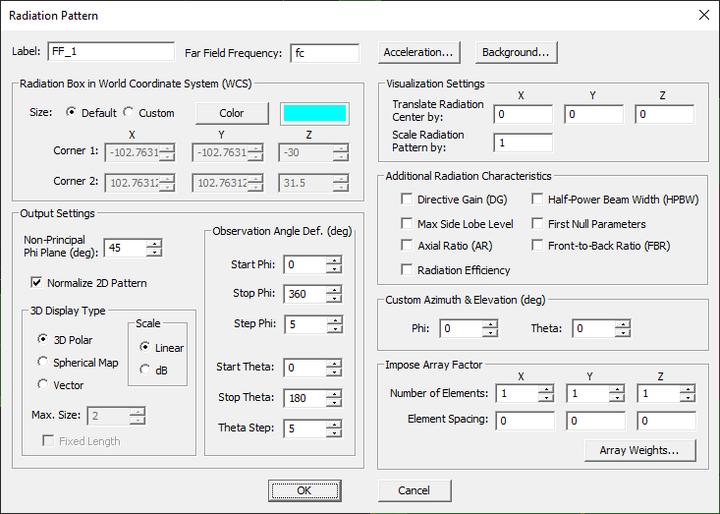
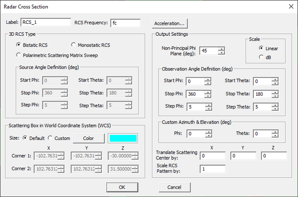
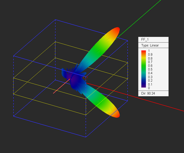
Far fields are typically computed in the spherical coordinate system as functions of the elevation and azimuth observation angles θ and φ. Only far-zone electric fields are normally considered. When your physical structure is excited using a lumped source, a waveguide source, a distributed source, a short dipole source, or an array of such sources, the far fields represent the radiation pattern of your source(s) in the far zone. In that case, you need to define a Radiation Pattern - Far Field Observable for your project. When your physical structure is illuminated by a plane wave source or a Gaussian beam source, the far fields represent the scattered fields. In the case of a plane source, you can compute the radar cross section (RCS) of your target structure. In that case, you need to define an RCS - Far Field Observable for your project.
In the FDTD method, the far fields are calculated using a near-field-to-far-field transformation of the field quantities on a given closed surface. EM.Tempo uses rectangular boxes to define these closed surfaces. You can use EM.Tempo's default radiation box or define your own custom box. Normally, the radiation box must enclose the entire FDTD structure. In this case, the calculated radiation pattern corresponds to the entire radiating structure. Alternatively, you can define a custom radiation box that may contain only parts of a structure, which results in a partial radiation pattern.
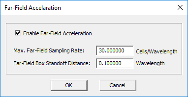
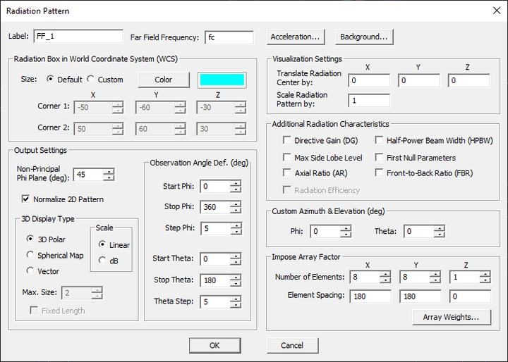
The default radiation box is placed at an offset of 0.1λ0 from the largest bounding box of your physical structure. You can change the offset value from the "Far Field Acceleration" dialog, which can be accessed by clicking the Acceleration... button of EM.Tempo's Radiation Pattern dialog. Calculation of far-field characteristics at high angular resolutions can be a very time consuming computational task. You can accelerate this process by setting a lower Max. Far Field Sampling Rate from the same dialog. The default sampling rate is 30 samples per wavelength. A low sampling rate will under-sample the mesh grid points on the radiation box.
Radiation Pattern Above a Half-Space Medium
In EM.Tempo, you can use CPML boundary conditions with zero offsets to model a structure with infinite lateral extents. The calculation of the far fields using the near-field-to-far-field transformation requires the dyadic Green's function of the background structure. By default, the FDTD engine uses the free space dyadic Green's function for the far field calculation. In general, the EM.Tempo provides the dyadic Green's functions for four scenarios:
- Free space background
- Free space background terminated in an infinite PEC ground plane at the bottom
- Free space background terminated in an infinite PMC ground plane at the bottom
- Free space background terminated in an infinite dielectric half-space medium
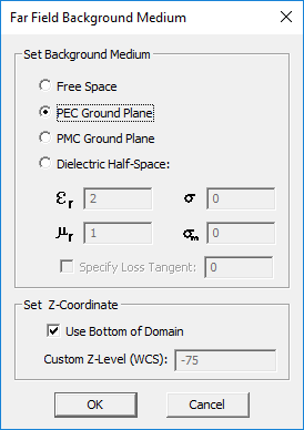
In other words, EM.Tempo lets you calculate the far field radiation pattern of a structure in the presence of any of the above four background structure types. You can set these choices in EM.Tempo's "Far Field Background Medium" dialog. To access this dialog, open the Radiation Pattern dialog and click the button labeled Background.... From this dialog, you can also set the Z-coordinate of the top of the terminating half-space medium. If you set the -Z boundary condition of your computational domain to PEC or PMC types, the cases of infinite PEC or PMC ground planes from the above list are automatically selected, respectively, and the Z-coordinates of the ground plane and the bottom face of the computational domain will be identical.
The fourth case applies when your computational domain ends from the bottom in a dielectric layer with a CPML -Z boundary along with a -Z domain offset equal to zero. If you set the lateral domain offset values along the ±X and ±Y directions equal to zero, too, , then your structure is, in effect, terminated at an infinite half-space dielectric medium. In that case, you have to specify the permittivity εr and electric conductivity σ of the terminating medium in the Background Medium dialog. You may additionally want to set the Z-coordinate of the top of that dielectric layer as the position of the interface between the free space and the lower dielectric half-space. Note that the current version of EM.Tempo does not calculate the far-field Green's function of a conductor-backed, dielectric substrate with a finite layer thickness. To use the background medium feature of EM.Tempo, your structure can have either an infinite PEC/PMC ground or a dielectric half-space termination.
Generating and Working with Multi-Frequency Simulation Data
One of the primary advantages of the FDTD method is its ability to run wideband EM simulations. The frequency domain data are computed by transforming the time-domain data to the Fourier domain. This is done automatically when EM.Tempo computes the port characteristics such as S/Z/Y parameters. The following frequency-domain observables are defined at a single frequency:
- Near-Field Sensor
- Far-field Radiation Pattern
- RCS
- Huygens Surface
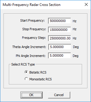
The default computation frequency of the above observables is the project's center frequency (fc). You can change the observable frequency from the observable's property dialog and enter any frequency in Hz. The reason these types of simulation data are computed at a single frequency is their typically very large size. However, you can define as many instances of these observables and set different frequency values for each one. In the case of radiation pattern and RCS, there are two dialogs that can be accessed from the navigation tree. Right-click on the "Fer-Field Radiation Patterns" or "Radar Cross Sections" items of the navigation tree and select Insert Multi-Frequency Radiation Pattern... or Insert Multi-Frequency RCS... from the contextual menu.
Using the multi-frequency dialogs, you can set the value of Start Frequency, Stop Frequency and Step Frequency in Hz. You can also set the values of Theta Angle Increment and Phi Angle Increment in degrees. The default values of both quantities are 5°. In the case of RCS, you have choose one of the two options: Bistatic RCS or Monostatic RCS.
To facilitate the process of all the defining multi-frequency observables in EM.Tempo, you can also use the following Python functions at the command line:
emag_field_sensor_multi_freq(f1,f2,df,dir_coordinate,x0,y0,z0)
emag_farfield_multi_freq(f1,f2,df,theta_incr,phi_incr)
emag_rcs_bistatic_multi_freq(f1,f2,df,theta_incr,phi_incr)
emag_rcs_monostatic_multi_freq(f1,f2,df,theta_incr,phi_incr)
emag_huygens_surface_multi_freq(f1,f2,df,x1,y1,z1,x2,y2,z2)
In the above Python functions, f1 and f2 are the start and stop frequencies, respectively, and df is the frequency increment, all expressed in Hz. Note that the above commands simply create and insert the specified observables in the navigation tree. They do not run perform a simulation. The created observables have the same "base name" with ordered numeric indices. For example, far-field radiation patterns are names as Multi_FF_1, Multi_FF_2, ...
EM.Tempo also provides some additional Python functions for the far-field radiation patterns and RCS observables.
emag_farfield_consolidate(x1,x2,dx,base_name)
emag_rcs_consolidate(x1,x2,dx,base_name)
emag_farfield_explode(base_name)
emag_rcs_explode(base_name)
emag_farfield_average(n,base_name)
emag_rcs_average(n,base_name)
The two "consolidate" Python functions take the results of multi-frequency simulation observables and merge them into a single data file. The base name in the case of far-field radiation patterns is "Multi_FF" as pointed out earlier. The name of the resulting consolidated data file is the same as the base name with a "_All" suffix and a ".DAT" file extension. In the case of far-field radiation patterns, it is "Multi_FF_All.DAT". The two "explode" Python functions take a consolidated data file names as "base_name_All.DAT" and break it up into several single-frequency ".RAD" or ".RCS" data files. Finally, the two "average" Python functions take several radiation pattern or RCS files with a common base name in the current project folder, compute their average and save the results to a new data file named "base_name_ave" with a ".RAD" or ".RCS" file extensions, respectively.
Generating the FDTD Mesh in EM.Tempo
EM.Tempo's Mesh Types
EM.Tempo generates a brick volume mesh for FDTD simulation. The FDTD mesh is a rectangular Yee mesh that extends to the entire computational domain. It is primarily constructed from three mesh grid profiles in the XY, YZ and ZX principal planes. These projections together create a 3D mesh space consisting of a large number of cubic volume cells (voxels) carefully assembled in a way that approximates the shape of the original structure.
In EM.Tempo, you can choose one of the three FDTD mesh types:
- Adaptive Mesh
- Regular Mesh
- Fixed-Cell Mesh
EM.Tempo's default mesh generator produces an adaptive brick mesh of your physical structure, whose mesh resolution varies with the frequency. As the operating frequency of your project increases, the default Adaptive FDTD mesh generator creates a larger number of smaller voxels for a given physical structure. The adaptive mesh is optimized in such a way as to capture all the geometric details, curvatures and thin slanted plates or sheets, which often pose a challenge to staircase meshing. It usually provides a reasonably accurate discretization of most complex structures.
Occasionally, you may opt for a more regularized FDTD mesh with almost equal grid line spacings everywhere, but still with a frequency-dependent cell size. In that case, you can use EM.Tempo's Regular FDTD mesh generator, which is indeed a simplified version of its adaptive mesh generator. The regular FDTD mesh enforces only two criteria: minimum mesh density and absolute minimum grid spacing. The grid cell sizes in this mesh are almost uniform in objects of the same material composition or in free-space regions.
EM.Tempo also offers a uniform, frequency-independent, Fixed-Cell FDTD mesh generator. The fixed-cell mesh consists of three uniform grids in the XY, YZ and ZX principal planes. However, the uniform mesh cell dimensions along the three direction, i.e. Δx, Δy and Δz do not have to be equal. The fixed-cell mesh generator tries to fit your physical structure to the mesh grid rather than adapting the mesh to your physical structure.
![]() Click here to learn more about Working with Mesh Generator.
Click here to learn more about Working with Mesh Generator.
![]() Click here to learn more about the properties of EM.Tempo's Adaptive Brick Mesh Generator.
Click here to learn more about the properties of EM.Tempo's Adaptive Brick Mesh Generator.
![]() Click here to learn more about the properties of EM.Tempo's Fixed-Cell Brick Mesh Generator.
Click here to learn more about the properties of EM.Tempo's Fixed-Cell Brick Mesh Generator.
Discretizing the Physical Structure Using the Adaptive Yee Mesh
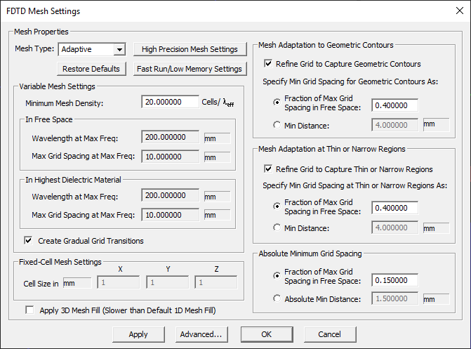
EM.Tempo's default mesh generator creates an adaptive brick volume mesh that uses a variable staircase profile, where the grid line spacings vary with the curvature (derivative) of the object edges or faces. As a result, a higher mesh resolution is produced at "curved" areas to better capture the geometrical details. The resolution of the adaptive FDTD mesh is driven by the Mesh Density, expressed in cells per effective wavelength. Since FDTD is a time-domain method and the excitation waveform may have a wideband spectral content, the effective wavelength is calculated based on the highest frequency of the project: fmax = f0 + Δf/2, where f0 (or fc) is your project's center frequency and Δf (or bw) is its specified bandwidth. In other words, the effective wavelength in the free space is λ0,eff = c / fmax, c being the speed of light in the free space. The effective wavelength in a dielectric material with relative permittivity εr and permeability μr is given by λd,eff = λ0,eff / √εrμr.
The adaptive FDTD mesh, by default, produces different grid cell sizes in the free space regions than inside dielectric regions. The effective wavelength in a dielectric material with relative permittivity er and permeability µr is given by λd,eff = λ0,eff / √εrμr. Therefore, the average ratio of the cell size in a dielectric region to the cell size in the free space is 1/√(εrμr). The adaptive FDTD mesh generator also takes note of the geometrical features of the objects it discretizes. This is more visible in the case of curved solids, curves surfaces and curved wires or obliquely oriented planes and lines which need to be approximated using a staircase profile. The mesh resolution varies with the slope of the geometrical shapes and tries to capture the curved segments in the best way. Another important feature of the adaptive FDTD mesher is generation of gradual grid transitions between low-density and high-density mesh regions. For example, this often happens around the interface between the free space and high permittivity dielectric objects. Gradual mesh transitions provide better accuracy especially in the case of highly resonant structures.
A carefully calculated, "Adaptive" mesh of your physical structure is generated in order to satisfy the following criteria:
- Optimize the number of mesh cells in each dimension. The product of the number of cells in all the three dimension determines the total mesh size. The larger the mesh size, the longer the simulation time, especially with the CPU version of the FDTD engine. Also, a very large mesh size requires more RAM, which may exceed your GPU memory capacity. Set the Minimum Mesh Density to a moderately low value to keep the mesh size manageable, but be careful not to set it too low (see the next item below).
- Ensure simulation accuracy by requiring an acceptable minimum number of cells per wavelength through each object and in the empty (free) space between them and the computational domain boundaries. An effective wavelength is defined for each material at the highest frequency of the project's specified spectrum. We recommend a Minimum Mesh Density of at least 15-20 cells/ wavelength. But for some resonant structures, 25 or even 30 cells per wavelength may be required to achieve acceptable accuracy. As you reduce the mesh density, the simulation accuracy decreases.
- Accurately represent and approximate the boundaries of edges or surfaces that are not grid-aligned by closely adhering to their geometric contours. This is controlled by the Minimum Grid Spacing Over Geometric Contours, which can be specified either as a fraction of the free space grid spacing or as an absolute length value in project units.
- Maximize the minimum grid spacing in any dimension inside the computational domain and thus maximize the simulation time step. The time step size is dictated by the CFL stability criterion and is driven by the smallest grid spacing in each dimension. The smaller the time step, the larger the number of time steps required for convergence. This is controlled using the Absolute Minimum Grid Spacing, which can be specified either as a fraction of the free space grid spacing or as an absolute value. It is critical to accurately represent and precisely maintain the object edge/surface boundaries in certain structures like resonant antennas and filters, as the phase of the reflected fields/waves is affected by the object boundary positions. When object boundaries are very close to each other, the mesh needs to represent them by two separate, but very closely spaced, grid lines. To control the minimum allowed grid spacing, use the Absolute Minimum Grid Spacing settings,
- Maintain a smooth grid with no abrupt jumps from low-density to high-density regions. This feature is enabled with the Create Gradual Grid Transitions check box (always checked by default).
When EM.Cube generates an FDTD mesh, a large number of geometrical considerations are taken into account. These include the bounding box of each object and its corners, the ends of a line, the apex of a cone or pyramid, or the locations of lumped sources, field probes and sensors, vertices of plane wave or far field boxes, to name a few examples. These points are “locked” as fixed grid nodes in the FDTD mesh. EM.Cube determines these points internally to generate a mesh that best approximates the original structure. As you saw earlier, you can use the FDTD mesh settings to control the shape and resolution of the mesh, for example, around the curved portions of your structure, or on slanted lines or faces, etc. These settings are global and apply to all the objects making up your physical structure.
You can control the global mesh more selectively using the Advanced FDTD Mesh Settings Dialog. To open this dialog, click the Advanced button at the bottom of the FDTD Mesh Settings dialog. For example, you can control the quality of the gradual grid transitions by setting the value of Max Adjacent Cell Size Ratio. The default value of this parameter is 1.3, which maintains a smooth grid line spacing scheme with no more than 1:1.3 ratio for adjacent cells. By default, grid lines are enforced at all source and observable locations. You have the option to disable this feature and round up source locations to their closest grid lines. You may also uncheck the box labeled "Adapt mesh resolution to material properties". In that case, the same effective wavelength will be used to determine the mesh resolution inside all materials as well as the free-space regions.
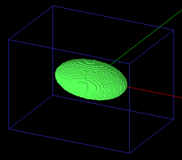
The figures below compare the three types of the FDTD mesh for a dielectric ellipsoid with εr = 4. Note that the cell size inside the dielectric region is half the cell size in the air region.
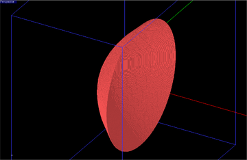
The figures below compare the low resolution and high resolution adaptive FDTD meshes of a PEC parabolic reflector. This structure involves both a curved surface and a very thin surface.
Adding Fixed Grid Points to the Adaptive Yee Mesh
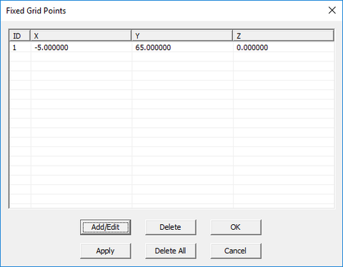
Adding fixed grid points to an FDTD mesh increases its resolution locally. Each fixed grid point adds three grid lines along the three principal axes passing through that point. You can add as many fixed grid points as you desire and create dense meshes at certain regions. Fixed grid points appear as grey points in the project workspace. To insert a new fixed grid point, follow these steps:
- Open the Fixed Grid Points Dialog by selecting Menu > Simulate > Discretization > Fixed Grid Points... or by right-clicking on the FDTD Mesh item of the navigation tree and selecting Fixed Grid Points Settings...
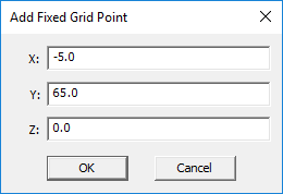
- Click the Add/Edit button to open the "Add Fixed Grid Point" dialog.
- Enter the (X, Y, Z) coordinates of the new fixed point in the coordinate boxes and click the OK button.
- To modify the coordinates of an existing fixed grid point, select it from the table and click the Add/Edit button.
- You can also remove a fix grid point from the FDTD mesh using the Delete button.
According to the Courant-Friedrichs-Levy (CFL) stability criterion, the FDTD time step is determined by the smallest cell size in your FDTD mesh. Occasionally, EM.Tempo's adaptive mesh generator may create extremely tiny grid cells that would result in extremely small time steps. This would then translate into a very long computation time. EM.Cube offers the "Regular" FDTD mesh generator, which is a simplified version of the adaptive mesh generator. In a regular FDTD mesh, the grid cell sizes stay rather the same in objects of the same material composition. The mesh resolution increases in materials of higher permittivity and/or permeability based on the effective wavelength in exactly the same way as the adaptive mesh.
Profiling the Brick Mesh
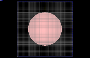
A volumetric brick mesh is overwhelming for visualization in the 3D space. For this reason, EM.Cube's mesh view shows only the outline of the cells on exterior surface of the (staircased) meshed objects. The mesh grid planes provide a 2D profile of the mesh cells along the principal coordinate planes. To display a mesh grid plane, select Menu > Simulate > Discretization > Grid Planes > and pick one of the three options: XY Plane, YZ Plane or ZX Plane. You may also right click on one of the XY Plane, YZ Plane or ZX Plane items in the Discretization section of the navigation tree and select Show from the contextual menu.
While a mesh grid plane is visible, you can move it back and forth between the two boundary planes at the two opposite sides of the computational domain. You can do this in one of the following four ways:
- Using the keyboard's Page Up PgUp key and Page Down PgDn key.
- By selecting Menu > Simulate > Discretization > Grid Planes > Increment Grid or Decrement Grid.
- By right clicking on one of the XY Plane, YZ Plane or ZX Plane items in the Discretization section of the navigation tree and selecting Increment Grid or Decrement Grid from the contextual menu.
- Using the keyboard shortcut > or <.
As you “step through” or profile the mesh grid, you can see how the structure is discretized along internal planes of the computational domain.
The FDTD Grid Coordinate System (GCS)
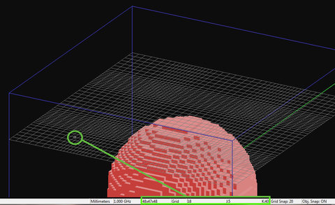
When your physical structure is discretized using the brick mesh generator, a second coordinate system becomes available to you. The mesh grid coordinate system allows you to specify any location in the computational domain in terms of node indices on the mesh grid. EM.Cube displays the total number of mesh grid lines of the simulation domain (Nx × Ny × Nz) along the three principal axes on the Status Bar. Therefore, the number of cells in each direction is one less than the number of grid lines, i.e. (Nx-1)× (Ny-1) × (Nz-1). The lower left front corner of the domain box (Xmin, Ymin, Zmin) becomes the origin of the mesh grid coordinate system (I = 0, J = 0, K = 0). The upper right back corner of the domain box (Xmax, Ymax, Zmax) therefore becomes (I = Nx-1, J = Ny-1, K = Nz-1).
EM.Cube allows you to navigate through the mesh grid and evaluate the grid points individually. Every time you display one of the three mesh grid planes, the "Grid Coordinate System (GCS)" is automatically activated. On the Status Bar, you will see ![]() instead of the default
instead of the default ![]() . This means that the current coordinates reported on Status Bar are now expressed in grid coordinate system. The current grid point is displayed by a small white circle on the current mesh grid plane, and it always starts from (I = 0, J = 0, K = 0). Using the keyboard's Arrow Keys, you can move the white circle through the mesh grid plane and read the current node's (I, J, K) indices on the status bar. You can switch back to the "World Coordinate System (WCS)" or change to the "Domain Coordinate System" by double-clicking the status bar box that shows the current coordinate system and cycling through the three options. The domain coordinate system is one that establishes its origin at the lower left front corner of the computational domain and measure distances in project unit just like the WCS.
. This means that the current coordinates reported on Status Bar are now expressed in grid coordinate system. The current grid point is displayed by a small white circle on the current mesh grid plane, and it always starts from (I = 0, J = 0, K = 0). Using the keyboard's Arrow Keys, you can move the white circle through the mesh grid plane and read the current node's (I, J, K) indices on the status bar. You can switch back to the "World Coordinate System (WCS)" or change to the "Domain Coordinate System" by double-clicking the status bar box that shows the current coordinate system and cycling through the three options. The domain coordinate system is one that establishes its origin at the lower left front corner of the computational domain and measure distances in project unit just like the WCS.
Running FDTD Simulations in EM.Tempo
EM.Tempo's Simulation Modes
Once you build your physical structure in the project workspace and define an excitation source, you are ready to run an FDTD simulation. The simulation engine will run even if you have not defined any observables. Obviously, no simulation data will be generated in that case. EM.Tempo currently offers several different simulation modes as follows:
| Simulation Mode | Usage | Number of Engine Runs | Frequency | Restrictions |
|---|---|---|---|---|
| Wideband Analysis | Simulates the physical structure "As Is" | Single run | Generates data for many frequency samples | None |
| Parametric Sweep | Varies the value(s) of one or more project variables | Multiple runs | Runs at the center frequency fc | None |
| Optimization | Optimizes the value(s) of one or more project variables to achieve a design goal | Multiple runs | Runs at the center frequency fc | None |
| HDMR Sweep | Varies the value(s) of one or more project variables to generate a compact model | Multiple runs | Runs at the center frequency fc | None |
| Dispersion Sweep | Varies the value of wavenumber in a periodic structure | Multiple runs | Runs at multiple frequency points corresponding to constant wavenumber values | Only for periodic structures excited by a plane wave source |
Running a Wideband FDTD Analysis
The FDTD method is one of the most versatile numerical techniques for solving electromagnetic modeling problems. Choosing the right settings and optimal values for certain numerical parameters will have a significant impact on both accuracy and computational efficiency of an FDTD simulation. Below are a number of steps that you should typically follow by order when planning your FDTD simulation:
- Identify material types and proper domain boundary conditions.
- Identify the source type and excitation mechanism.
- Define the project observables.
- Mesh the physical structure and examine the quality of the generated mesh and it geometric fidelity.
- Determine the proper temporal waveform.
- Select the simulation mode and run the FDTD engine.
Wideband analysis is EM.Tempo's simplest and most straightforward simulation mode. It runs the FDTD time marching loop once. At the end of the simulation, the time-domain field data are transformed into the frequency domain using a discrete Fourier transform (DFT). As a result, you can generate wideband frequency data from a single time-domain simulation run. The other simulation modes will be explained later in this manual.
To open the Simulation Run Dialog, click the Run ![]() button of the Simulate Toolbar or select the menu item Simulate → Run... from the menu bar or use the keyboard shortcut Ctrl+R. To start the FDTD simulation, click the Run button at the bottom of this dialog. Once the simulation starts, the "Output Message Window" pops up and reports messages during the different stages of the FDTD simulation. During the FDTD time marching loop, after every 10th time step, the output window updates the values of the time step, elapsed time, the engine performance in Mega-cells per seconds, and the value of the convergence ratio Un/Umax in dB. An EM.Tempo simulation is terminated when the ratio Un/Umax falls below the specified power threshold or when the maximum number of time steps is reached. You can, however, terminate the FDTD engine earlier by clicking the Abort Simulation button.
button of the Simulate Toolbar or select the menu item Simulate → Run... from the menu bar or use the keyboard shortcut Ctrl+R. To start the FDTD simulation, click the Run button at the bottom of this dialog. Once the simulation starts, the "Output Message Window" pops up and reports messages during the different stages of the FDTD simulation. During the FDTD time marching loop, after every 10th time step, the output window updates the values of the time step, elapsed time, the engine performance in Mega-cells per seconds, and the value of the convergence ratio Un/Umax in dB. An EM.Tempo simulation is terminated when the ratio Un/Umax falls below the specified power threshold or when the maximum number of time steps is reached. You can, however, terminate the FDTD engine earlier by clicking the Abort Simulation button.
The FDTD Simulation Engine Settings
An FDTD simulation involves a number of numerical parameters that can be accessed and modified from the FDTD Engine Settings Dialog. To open this dialog, select Menu > Simulate > Simulation Engine Settings... or open the Run Dialog, and click the Settings button next to the engine dropdown list.
In the " Convergence " section of the dialog, you can set the Termination Criterion for the FDTD time loop. The time loop must stop after a certain point in time. If you use a decaying waveform like a Gaussian pulse or a Modulated Gaussian pulse, after certain number of time steps, the total energy of the computational domain drops to very negligible values, and continuing the time loop thereafter would not generate any new information about your physical structure. By contrast, a sinusoidal waveform will keep pumping energy into the computational domain forever, and you have to force the simulation engine to exit the time loop. EM.Tempo provides two mechanism to terminated the time loop. In the first approach, an energy-like quantity defined as Un = Σ [ ε0|Ei,n|2 + μ0|Hi,n|2 ].ΔVi is calculated and recorded at a large random set of points in the computational domain. Here i is the space index and n is the time index. The quantity Un has a zero value at t = 0 (i.e. n = 0), and its value starts to build up over time. With a Gaussian or Modulated Gaussian pulse waveform, Un reach a maximum value Umax at some time step and starts to decline thereafter. The ratio 10.log( Un/ Umax) expressed in dB is used as the convergence criterion. When its value drops below certain Power Threshold, the time loop is exited. The default value of Power Threshold is -30dB, meaning that the FDTD engine will exit the time loop if the quantity Un drops to 1/1000 of its maximum value ever. The second termination criterion is simply reaching a Maximum Number of Time Steps , whose default value set to 10,000. A third option, which is EM.Tempo's default setting (labeled "Both"), terminates the simulation as soon as either of the first two criteria is met first.
| |
Keep in mind that for highly resonant structures, you may have to increase the maximum number of time steps to very large values above 20,000. |
The "Acceleration" section of the FDTD Simulation Engine Settings dialog give three options for the FDTD kernel:
- Serial CPU Solver
- Multi-Core CPU Solver
- GPU Solver
The serial CPU solver is EM.Tempo's basic FDTD kernel that run the time marching loop on a single central processing unit (CPU) of your computer. The default option is the multi-core CPU solver. This is a highly parallelized version of the FDTD kernel based on the Open-MP framework. It takes full advantage of a multi-core, multi-CPU architecture, if your computer does have one. The GPU solver is a hardware-accelerated FDTD kernel optimized for CUDA-enabled graphical processing unit (GPU) cards. If your computer has a fast NVIDIA GPU card with enough onboard RAM, the GPU kernel can speed up your FDTD simulations up to 50 times or more over the single CPU solver.
For structures excited with a plane wave source, there are two standard FDTD formulations: Scattered Field (SF) formulation and Total Field - Scattered Field (TF-SF) formulation. EM.Tempo offers both formulations. The TF-SF solver is the default choice and is typically much faster than the SF solver for most problems. In two cases, when the structure has periodic boundary conditions or infinite CPML boundary conditions (zero domain offsets), only the SF solver is available.
Modeling 3D Periodic Structures in EM.Tempo
EM.Tempo allows you to simulate doubly periodic structures with periodicities along the X and Y directions. In the FDTD method, this is accomplished by applying periodic boundary conditions (PBC) at the side walls of the computational domain.
| |
EM.Tempo can only handle regular, non-skewed periodic lattices with no secondary offsets. |
![]() Click here to learn more about the theory of Time Domain Simulation of Periodic Structures.
Click here to learn more about the theory of Time Domain Simulation of Periodic Structures.
Defining a Periodic Structure in EM.Tempo
By default, your physical structure in the project workspace is not periodic, and you have to instruct EM.Tempo to turn it into a periodic structure using its Periodicity Dialog. By designating a structure as periodic, you enforce periodic boundary conditions (PBC) on the side walls of its computational domain. Your structure in the project workspace then turns into a periodic unit cell. The periodic side walls are displayed with dashed blues lines.
To define a periodic structure, follow these steps:
- Select Menu > Simulate > Computational Domain > Periodicity Settings... or right click on the Periodicity item in the Computational Domain section of the Navigation Tree and select Periodicity Settings... from the contextual menu. This open up the Periodicity Settings Dialog.
- Check the box labeled Periodic Structure and click the Apply button of this dialog. The default domain box initially shrinks to the edges of the physical structure in the project workspace. The default periods along the X and Y axes appear in the dialog, which are equal to the dimensions of the structure's bounding box.
- Enter new values for X Spacing and Y Spacing in project units and close the dialog.
- Periodic boundary conditions (PBC) are established on the ±X and ±Y faces of the domain box. You still have to designate the boundary conditions on the ±Z faces of the computational domain. These are CPML by default. But you can change them to PEC or PMC.
Exciting Periodic Structures as Radiators in EM.Tempo
In EM.Tempo, a periodic structure can be excited using various source types. Exciting the unit cell structure using a lumped source, a waveguide source, or a distributed source, you can model an infinite periodic antenna array. For most practical antenna types, you excite your periodic structure with a lumped source or waveguide source. In this case, you can define a port for the lumped source or waveguide source and calculate the S11 parameter or input impedance of the periodic antenna array. You can also compute the near-field and far-field data.
EM.Tempo's periodic FDTD simulator uses periodic boundary conditions (PBC) to model an infinite periodic array. All the periodic replicas of the unit cell structure are excited. In this case, you can impose a phase progression across the infinite array to steer its beam. You can do this from the property dialog of the lumped source or waveguide source. At the bottom of the Lumped Source Dialog or Waveguide Source Dialog, there is a section titled Periodic Beam Scan Angles. This section is grayed out when the project structure is not periodic. You can enter desired beam scan angle values for both Theta and Phi in degrees. To visualize the radiation pattern of the beam-steered array, you have to define a finite-sized array factor. You do this in the "Impose Array Factor" section of the Radiation Pattern Dialog.
| |
For large θ scan angles, the periodic FDTD time marching loop may take far more time steps to converge. |
Exciting Periodic Structures Using Plane Waves in EM.Tempo
Using a plane wave source to excite a periodic structure in EM.Tempo, you can model frequency selective surfaces, electromagnetic band-gap (EBG) structures, metamaterials, etc. Exciting periodic structures with plane wave sources requires careful attention. EM.Tempo's FDTD simulation engine uses the direct spectral domain FDTD or constant transverse wavenumber method for analyzing periodic structures. In this technique, instead of a plane wave box, one defines a plane wave surface parallel to the X-Y plane. At the end of the FDTD simulation of a periodic structure with plane wave excitation, the reflection and transmission coefficients of the structure are calculated and saved into ASCII data files.
Using a plane wave source to excite a periodic structure in EM.Tempo, you can model frequency selective surfaces, electromagnetic band-gap (EBG) structures, metamaterials, etc. Exciting periodic structures with plane wave sources requires careful attention. EM.Tempo's FDTD simulation engine uses the direct spectral domain FDTD or constant transverse wavenumber method for analyzing periodic structures. In this technique, instead of a plane wave box, one defines a plane wave surface parallel to the X-Y plane. If the plane wave source illuminates the periodic unit cell from the top (90° < θ < 180°), the excitation surface is placed above the structure's bounding box. If the plane wave source illuminates the periodic unit cell from the bottom up (0° < θ < 90°), the excitation surface is placed below the structure's bounding box. In either case, the plane wave must intercept the excitation surface before hitting the unit cell's physical structure. It is highly recommended that you accept EM.Tempo's default settings for the plane wave box of periodic structures. Nevertheless, you can change the location of the excitation surface if you wish. To do so, you have to open the Plane Wave Dialog. In the Excitation Box section of the dialog, select the Size: Custom option. Only the Z Coordinate of Corner 1 is available for editing. The rest of the coordinates are enforced by the periodic domain. You can enter the incidence angles Theta and Phi in degrees. For periodic structures, only the TMz and TEz polarization options are available.
One of the pitfalls of the direct spectral FDTD method is the possibility of horizontal resonances, which may lead to indefinite oscillation or even divergence of field values during the time marching loop. This happens in the case of oblique plane wave incidence when θ > 0°. EM.Cube's FDTD engine automatically detects such cases and avoids those resonances by shifting the modulation frequency of the modulated Gaussian pulse waveform away from the resonant frequency. However, in some cases, the size of oscillations may still remain large after a large number of time steps. Occasionally, a late-time diverging behavior may appear. To avoid situations like these, it is highly recommended that you place a time-domain field probe above your structure and monitor the temporal field behavior during the time marching loop as shown in the figure below.
| |
It is very important to keep in mind that only in the case of normal incidence does EM.Cube compute the reflection and transmission coefficients over the entire specified bandwidth of the project. At oblique incidences when θ > 0, the computed R/T coefficients after the discrete Fourier transformation are valid only at the center frequency of the project for the given value of the incident θ0 angle. In other words, the computed R/T coefficients at all the other frequencies away from the center frequency correspond to different values of the incident θ angle. As a result, EM.Cube only saves the reflection and transmission coefficients at the center frequency into the output data files "reflection_coefficient.CPX" and "transmission_coefficient.CPX". |
Running a Dispersion Sweep in EM.Tempo
The Dispersion Sweep option of the Simulation Mode drop-down list performs a sweep of constant kl wavenumber values. This is a specialized sweep for the constant transverse wavenumber method that EM.Tempo uses to model periodic structures illuminated by a plane wave source. The real advantage of a dispersion sweep is that through a one-dimensional sweep of kli, you can find the reflection and transmission coefficients for all combinations of frequency fj and incident angle θj such that (2π/c) . fj. sin θj = kli. This provides a complete picture of the dispersion behavior of your periodic structure. The sweep data can be graphed as a wavenumber-frequency intensity plot (also known as beta-k diagram) that projects the eigenvalues of the periodic structure. The horizontal axis represents the constant transverse wavenumber kl (or beta). The vertical axis represents frequency. Sometimes, the free space wave number k0 = (2π/c).f is used as the vertical axis, hence, the term beta-k diagram. However, EM.Cube plots frequency vs. wavenumber. Both the horizontal and vertical axes start from 0 and extend to fmax and kl,max, respectively, where fmax = f0 + Δf/2, and Δf is the specified bandwidth of the project. For this sweep option you have to specify the number of wavenumber samples. Note that the dispersion sweep is run for a fixed given value of the plane wave incident angle φ as specified in EM.Tempo's Plane Wave Dialog.

