Glossary of EM.Cube's Materials, Sources, Devices & Other Physical Object Types
Contents
- 1 Active Distributed One-Port Device
- 2 Active Distributed Two-Port Device
- 3 Active Lumped One-Port Device
- 4 Active Lumped Two-Port Device
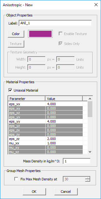
- 5 Anisotropic Material
- 6 Capacitor
- 7 Coaxial Port
- 8 Conductive Sheet Trace
- 9 Coplanar Waveguide (CPW) Port
- 10 Dielectric Material
- 11 Diode
- 12 Dispersive Material
- 13 Distributed Source
- 14 Embedded Dielectric Object Set
- 15 Embedded PEC Via Set
- 16 Ferrite Material
- 17 Filamentary Current Source
- 18 Fixed-Potential PEC
- 19 Fixed-Temperature PTC
- 20 Gaussian Beam
- 21 Gyrotropic Material
- 22 Hertzian Short Dipole Source
- 23 Huygens Source
- 24 Impedance/Dielectric Surface
- 25 Impenetrable Surface
- 26 Inductor
- 27 Lumped Source
- 28 Magnetoplasma Material
- 29 Microstrip Port
- 30 Parallel RC Device
- 31 Penetrable Surface
- 32 Penetrable Volume
- 33 Perfect Electric Conductor (PEC)
- 34 Perfect Magnetic Conductor (PMC)
- 35 Permanent Magnet
- 36 Plane Wave
- 37 Point Radiator Set
- 38 Point Scatterer Set
- 39 Point Transmitter Set
- 40 Probe Gap Circuit Load
- 41 Probe Gap Circuit Source
- 42 Resistor
- 43 Scattering Wave Port
- 44 Series RL Device
- 45 Slot Trace
- 46 Strip Gap Circuit Load
- 47 Strip Gap Circuit Source
- 48 Terrain Surface
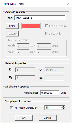
- 49 Thin Wire
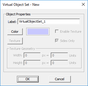
- 50 Virtual Object Group
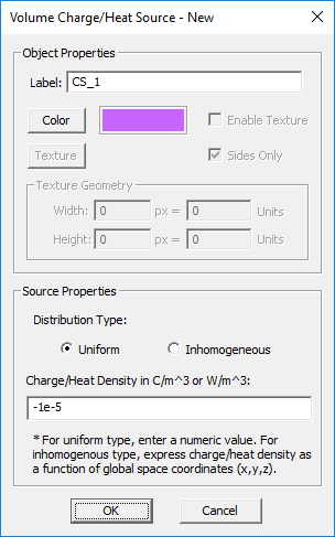
- 51 Volume Charge
- 52 Volume Current
- 53 Volume Heat Source
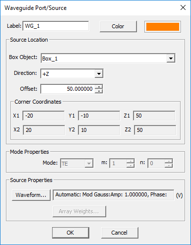
- 54 Waveguide Port
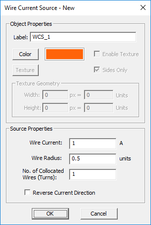
- 55 Wire Current
- 56 Wire Gap Circuit Load
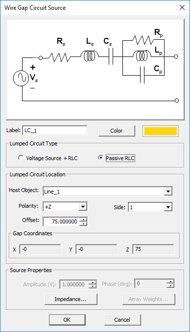
- 57 Wire Gap Circuit Source
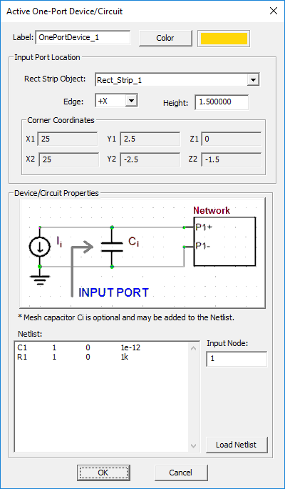
Active Distributed One-Port Device
MODULE: EM.Tempo
FUNCTION: Places an active distributed one-port device or circuit with a Netlist definition at an edge of a specified strip object that is parallel to one of the three principal axes
TO DEFINE AN ACTIVE DISTRIBUTED ONE-PORT DEVICE:
- Right-click on the Active One-Ports item in the navigation tree.
- Select Insert New Source... to open up the Active One-Port Device/Circuit Dialog.
- From the Rect Strip drop-down list, select a rectangle strip object. Note that only strip objects parallel to one of the three principal axes are listed.
- Select one of the edges of the rectangle strip where you want to place the active device.
- Enter a value for Height in project units. This is the height of the microstrip transmission line above its ground plane. It determines the size of the "active sheet".
- Enter the Netlist description of the device in the dialog's text editor.
- Alternatively, you can import an existing external Netlist file with a ".CIR" or ".TXT" file extension using the Load Netlist button.
- In the box labeled Input Node, enter the circuit node used in the Netlist that corresponds to the physical microstrip port. The ground is assumed to be Node 0.
- Click the OK button of the dialog to return to the project workspace.
PYTHON COMMAND: distributed_one_port(label,rect_object,height,edge,netlist_filename,input_node)
ACTIVE DISTRIBUTED ONE-PORT DEVICE PARAMETERS
| Parameter Name | Value Type | Units | Default Value | Notes |
|---|---|---|---|---|
| height | real numeric | project units | 1.5 | the height of the microstrip transmission line above its ground plane |
| input_port | integer numeric | - | 1 | Netlist circuit node that is connected to the FDTD mesh |
Active Distributed Two-Port Device
MODULE: EM.Tempo
FUNCTION: Places an active distributed two-port device or circuit with a Netlist definition at the edges of two specified strip objects that are both parallel to one of the three principal axes
TO DEFINE AN ACTIVE DISTRIBUTED TWO-PORT DEVICE:
- Right-click on the Active Two-Ports item in the navigation tree.
- Select Insert New Source... to open up the Active Two-Port Device/Circuit Dialog.
- In the Input and Output Port sections of the dialog, select two distinct rectangle strip objects from the two Rect Strip drop-down lists. Note that only strip objects parallel to one of the three principal axes are listed.
- Select one of the edges of each rectangle strip where you want to place the input and output ports of the active device.
- Enter a value for Height in project units. This is the height of the two microstrip transmission lines above their common ground plane. It determines the size of the two "active sheets".
- Enter the Netlist description of the two-port device in the dialog's text editor.
- Alternatively, you can import an existing external Netlist file with a ".CIR" or ".TXT" file extension using the Load Netlist button.
- In the boxes labeled Input Node and Output Node, enter the circuit nodes used in the Netlist that corresponds to the two physical microstrip ports. The ground is assumed to be Node 0.
- Click the OK button of the dialog to return to the project workspace.
PYTHON COMMAND: distributed_two_port(label,rect_object_1,height_1,edge_1,rect_object_2,height_2,edge_2,netlist_filename,input_node,output_node)
ACTIVE DISTRIBUTED TWO-PORT DEVICE PARAMETERS
| Parameter Name | Value Type | Units | Default Value | Notes |
|---|---|---|---|---|
| height_1 | real numeric | project units | 1.5 | the height of the input microstrip transmission line above its ground plane |
| height_2 | real numeric | project units | 1.5 | the height of the output microstrip transmission line above its ground plane |
| input_port | integer numeric | - | 1 | Netlist circuit node that is connected to the FDTD mesh at Port 1 |
| output_port | integer numeric | - | 2 | Netlist circuit node that is connected to the FDTD mesh at Port 2 |
Active Lumped One-Port Device
MODULE: EM.Tempo
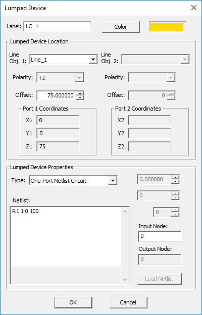
FUNCTION: Places a lumped active one-port device or circuit with a Netlist definition at a specified point on a PEC line object that is parallel to one of the three principal axes
TO DEFINE AN ACTIVE LUMPED ONE-PORT DEVICE:
- Right-click on the Lumped Devices item in the navigation tree.
- Select Insert New Source... to open up the Lumped Device Dialog.
- From the Host drop-down list, select a line object. Note that only lines parallel to one of the three principal axes are listed.
- From the Type drop-down list, select One-Port Netlist Circuit.
- By default, the lumped device is placed at the midpoint of the host line object. You can modify the Offset parameter, which is measured from the start point of the line and is always positive.
- Enter the Netlist definition of your one-port circuit in the box labeled Netlist'.
- Alternatively, you can import a Netlist text file. Click the Load Netlist button of the dialog. The standard Windows Open dialog opens up. You can import text files with a ".CIR" or ".TXT" file extension.
- Enter an integer value for Input Node of your circuit. The device will be connected to the FDTD mesh at the specified input node and the ground node (0).
- Click the OK button of the dialog to return to the project workspace.
PYTHON COMMAND: lumped_one_port(label,line_object,offset,netlist_filename,input_node)
ACTIVE LUMPED ONE-PORT DEVICE PARAMETERS
| Parameter Name | Value Type | Units | Default Value | Notes |
|---|---|---|---|---|
| offset | real numeric | project units | half the length of host line object | distance between the device and the start point of the host line object |
| input_port | integer numeric | - | 1 | Netlist circuit node that is connected to the FDTD mesh |
Active Lumped Two-Port Device
MODULE: EM.Tempo
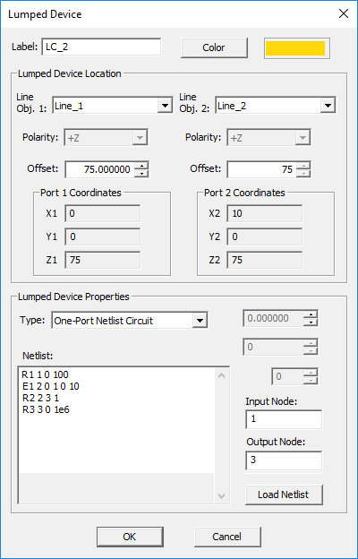
FUNCTION: Places a lumped active two-port device or circuit with a Netlist definition at a specified point on a PEC line object that is parallel to one of the three principal axes
TO DEFINE AN ACTIVE LUMPED ONE-PORT DEVICE:
- Right-click on the Lumped Devices item in the navigation tree.
- Select Insert New Source... to open up the Lumped Device Dialog.
- From the Host Obj. 1 drop-down list, select a line object. Note that only lines parallel to one of the three principal axes are listed.
- From the Type drop-down list, select Two-Port Netlist Circuit.
- For a two-port device, you need to select a second host line from the drop-down list labeled Host Obj. 2.
- By default, the lumped device is placed at the midpoint of the host line object. You can modify the two Offset parameters, which are measured from the start point of the host lines and are always positive.
- Enter the Netlist definition of your two-port circuit in the box labeled Netlist'.
- Alternatively, you can import a Netlist text file. Click the Load Netlist button of the dialog. The standard Windows Open dialog opens up. You can import text files with a ".CIR" or ".TXT" file extension.
- Enter two integer values for Input Node' and Output Node of your circuit. The two-pot device will be connected to the FDTD mesh at the specified input and output nodes and the ground node (0).
- Click the OK button of the dialog to return to the project workspace.
PYTHON COMMAND: lumped_two_port(label,line_object_1,offset_1,line_object_2,offset_2,netlist_filename,input_node,output_node)
ACTIVE LUMPED TWO-PORT DEVICE PARAMETERS
| Parameter Name | Value Type | Units | Default Value | Notes |
|---|---|---|---|---|
| offset1 | real numeric | project units | half the length of host line object | distance between Port 1 and the start point of the first host line object |
| offset2 | real numeric | project units | half the length of host line object | distance between Port 2 and the start point of the second host line object |
| input_port | integer numeric | - | 1 | Netlist circuit node that is connected to the FDTD mesh at Port 1 |
| output_port | integer numeric | - | 2 | Netlist circuit node that is connected to the FDTD mesh at Port 2 |
Anisotropic Material
MODULE: EM.Tempo
FUNCTION: Defines an isotropic material object group with four constitutive tensors
TO DEFINE AN ANISOTROPIC MATERIAL GROUP:
- Right-click on the Anisotropic Materials item in the navigation tree.
- Select Insert New Isotropic Material... to open up the Isotropic Material dialog.
- Click the OK button of the dialog to return to the project workspace.
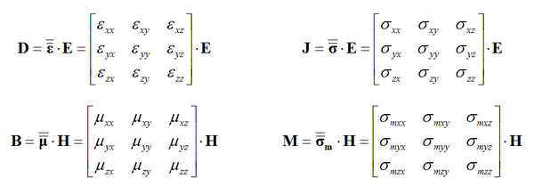
NOTES, SPECIAL CASES OR EXCEPTIONS: EM.Tempo allows you to define a general anisotropic material, whose constitutive parameters, i.e. permittivity (ε), permeability (μ), electrical conductivity (σ) and magnetic conductivity (σm), are all tensorial in nature. Each constitutive parameter in this case is represented by a 3×3 matrix:
A Uniaxial material is a special case of an anisotropic material whose constitutive parameters are all diagonal matrices. Specifying an anisotropic material as Uniaxial in the FDTD Module has a very important computational implication. There are six field update equations for uniaxial materials at each time steps: three for the electric field and three for the magnetic field. In this respect, a uniaxial material is similar to an isotropic dielectric material. On the other hand, a fully anisotropic material with non-zero off-diagonal constitutive matrix elements requires twelve update equations at each time step: three equations for the three components of each of the four vector fields E, D, H and B. As a result, the time loop for fully anisotropic materials takes much longer time than uniaxial materials.
PYTHON COMMAND: None
ANISOTROPIC MATERIAL PARAMETERS
| Parameter Name | Value Type | Units | Default Value | Notes |
|---|---|---|---|---|
| Locked mesh density | Real Numeric | cells/effective wavelength | 30 | Only if "Lock Mesh" enabled |
Capacitor
MODULE: EM.Tempo
FUNCTION: Places a capacitor at a specified point on a PEC line object that is parallel to one of the three principal axes
TO DEFINE A CAPACITOR:
- Right-click on the Lumped Devices item in the navigation tree.
- Select Insert New Source... to open up the Lumped Device Dialog.
- From the Host drop-down list, select a line object. Note that only lines parallel to one of the three principal axes are listed.
- From the Type drop-down list, select Capacitor.
- By default, the lumped device is placed at the midpoint of the host line object. You can modify the Offset parameter, which is measured from the start point of the line and is always positive.
- Enter a value for Capacitance in pF. The default capacitance is 1pF.
- Click the OK button of the dialog to return to the project workspace.
PYTHON COMMAND: capacitor(label,line_object,offset,capacitance_pF)
LUMPED CAPACITOR PARAMETERS
| Parameter Name | Value Type | Units | Default Value | Notes |
|---|---|---|---|---|
| offset | real numeric | project units | half the length of host line object | distance between the device and the start point of the host line object |
| capacitance | real numeric | pF | 1 | - |
Coaxial Port
MODULE: EM.Tempo
FUNCTION: Places a special distributed circular source of a specified width pointing away radially at one of the bases of a PEC cylinder object that is parallel to one of the three principal axes
TO DEFINE A COAXIAL PORT:
- Right-click on the Coaxial Ports item in the navigation tree of EM.Tempo.
- Select Insert New Source... to open up the Coaxial Port Dialog.
- From the Host drop-down list, select a cylinder object. Note that only PEC cylinder objects parallel to one of the three principal axes are listed.
- You have to specify the outer radius of the coaxial port, which is the same as the outer conductor radius of the coaxial transmission line. The inner conductor radius of the coaxial line is the same as the radius of the host cylinder object.
- A coaxial port can be placed at one of the two bases of the host cylinder. You can select the desired location from the Local Edge drop-down list.
- Click the OK button of the dialog to return to the project workspace.
PYTHON COMMAND: coaxial_src(label,cylinder_object,outer_radius,edge[,magnitude,phase,resistance])
COAXIAL PORT PARAMETERS
| Parameter Name | Value Type | Units | Default Value | Notes |
|---|---|---|---|---|
| outer radius | real numeric | project units | 2 * host cylinder radius | coaxial line's outer conductor radius |
| resistance | real numeric | Ohms | 50 | internal impedance of the distributed voltage source |
Conductive Sheet Trace
MODULE: EM.Picasso
FUNCTION: Defines a conductive sheet trace group
TO DEFINE A CONDUCTIVE SHEET GROUP:
- Right-click on the Conductive Sheet Traces item in the navigation tree.
- Select Insert New Conductive Sheet Trace... to open up the Conductive Sheet Trace dialog.
- Besides the color and texture properties, you have to enter values for the Electric Conductivity σ in S/m and the sheet Thickness in the project units.
- Click the OK button of the dialog to return to the project workspace.
NOTES, SPECIAL CASES OR EXCEPTIONS: In EM.Picasso, you may model imperfect metals using conductive sheet traces, which are an example of impedance surfaces. Keep in mind that you can typically model most lossless metallic traces such as micstorip lines and planar patches using PEC groups. A PEC trace is assumed to have an infinite electric conductivity and a zero metallization thickness. But also remember that since EM.Picasso's simulation engine is based on the 2.5-D method of moments (MoM), lossy embedded dielectric objects with a large σ cannot represent an imperfect metal because can only support vertical currents. A Conductive Sheet Trace group has a finite electric conductivity σ and a small nonzero finite thickness expressed in the project units.
The conductive sheet traces are modeled using the surface impedance boundary condition stated above. If the thickness of the sheet is greater than the skin depth of the metal at the project frequency, then the surface impedance is given by
- [math] Z_s = \dfrac{1+j}{\sigma \delta}, \quad \delta = \sqrt{\dfrac{2}{k_0 Z_0 \sigma}} [/math]
If the thickness t of the sheet is less than the skin depth, then the conductive sheet transition boundary condition is used instead, and the surface impedance is given by
- [math] Z_s = \dfrac{1}{[j k_0 Y_0 (\varepsilon_r - 1) + \sigma] \tau} = \dfrac{1}{\sigma_{tot} \tau} [/math]
PYTHON COMMAND: conductive_sheet_group(label,sigma,thickness)
CONDUCTIVE SHEET PARAMETERS
| Parameter Name | Value Type | Units | Default Value | Notes |
|---|---|---|---|---|
| sigma (σ) | Real Numeric | S/m | 5.8e+7 | electric conductivity |
| thickness | Real Numeric | project units | 1.0 | finite metallization thickness |
| Locked mesh density | Real Numeric | cells/effective wavelength | 30 | Only if "Lock Mesh" enabled |
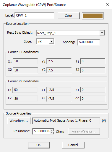
Coplanar Waveguide (CPW) Port
MODULE: EM.Tempo
FUNCTION: Places two coupled special distributed sources of a specified width pointing opposite directions on the two sides of one of the edges of a PEC rectangle strip object that is parallel to one of the three principal planes
TO DEFINE A CPW PORT:
- Right-click on the CPW Ports item in the navigation tree of EM.Tempo.
- Select Insert New Source... to open up the CPW Port Dialog.
- From the Host drop-down list, select a rectangle strip object. Note that only PEC rectangle strip objects parallel to one of the three principal planes are listed.
- You have to specify the width of the CPW port, which is the same as the slot width of the coplanar waveguide transmission line.
- A CPW port can be placed at one of the four edges of the host rectangle strip. You can select the desired location from the Edge drop-down list.
- Click the OK button of the dialog to return to the project workspace.
PYTHON COMMAND: cpw_src(label,rect_object,spacing,edge[,magnitude,phase,resistance])
CPW PORT PARAMETERS
| Parameter Name | Value Type | Units | Default Value | Notes |
|---|---|---|---|---|
| width | real numeric | project units | 5 | coplanar waveguide's slot width |
| resistance | real numeric | Ohms | 50 | internal impedance of the distributed voltage source |
Dielectric Material
MODULE: EM.Tempo, EM.Ferma, EM.Libera
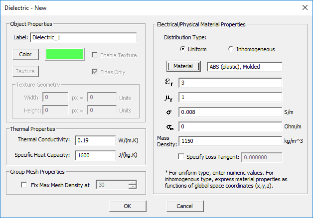
FUNCTION: Defines a dielectric material object group with specified constitutive parameters
TO DEFINE A DIELECTRIC GROUP:
- Right-click on the Dielectric Materials or Dielectric Objects item in the navigation tree.
- Select Insert New Dielectric... to open up the New Dielectric Material dialog.
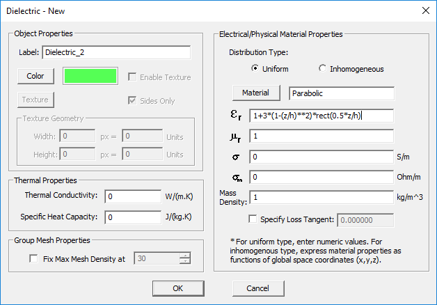
- You have two options to choose from: Uniform and Inhomogeneous.
- If you choose the uniform option, you have to enter numeric values for relative permittivity εr, electric conductivity σ in S/m, relative permittivity μr, magnetic conductivity σm in Ω/m and mass density in kg/m3. The default values are εr = μr = 1, σ = σm = 0, and ρV = 1. You can also enter numeric values for Thermal Conductivity in W/(m.K) and Specific Heat Capacity in J/(kg.K). These parameters are used for thermal simulation in EM.Ferma.
- If you choose the inhomogeneous option, you have to enter mathematical or Python expressions in the global (x,y,z) coordinates for all the constituent parameters.
- Change the color of the material group if necessary.
- Click the OK button of the dialog to return to the project workspace.
NOTES, SPECIAL CASES OR EXCEPTIONS: The inhomogeneous option is available only in EM.Tempo and EM.Ferma. Although in this mode you may enter numeric values as valid mathematical or Python expressions, beware of the fact that the Python expressions are evaluated at every single mesh point. This may take a very long processing time for large meshes.
PYTHON COMMAND: dielectric_group(label,eps,sigma,mu,sigma_m[,rr,gg,bb])
DIELECTRIC PARAMETERS
| Parameter Name | Value Type | Units | Default Value | Notes |
|---|---|---|---|---|
| eps (εr) | Real Numeric | - | 1.0 | relative permittivity |
| sigma (σ) | Real Numeric | S/m | 0.0 | electric conductivity |
| mu (μr) | Real Numeric | - | 1.0 | relative permeability |
| sigma_m (σm) | Real Numeric | Ohm/m | 0.0 | magnetic conductivity |
| loss_tangent | Real Numeric | - | 0.0 | dielectric loss tangent |
| mass_dens (ρV) | Real Numeric | kg/m3 | 1.0 | volume mass density |
| thermal_cond | Real Numeric | W/(m.K) | 0.0 | thermal conductivity |
| spec_cap | Real Numeric | J/(kg.K) | 0.0 | specific heat capacity |
| Locked mesh density | Real Numeric | cells/effective wavelength | 30 | Only if "Lock Mesh" enabled |
Diode
MODULE: EM.Tempo
FUNCTION: Places an nonlinear diode at a specified point on a PEC line object that is parallel to one of the three principal axes
TO DEFINE A DIODE:
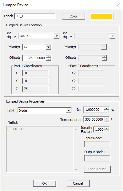
- Right-click on the Lumped Devices item in the navigation tree.
- Select Insert New Source... to open up the Lumped Device Dialog.
- From the Host drop-down list, select a line object. Note that only line parallel to one of the three principal axes are listed.
- From the Type drop-down list, select Diode.
- By default, the lumped device is placed at the midpoint of the host line object. You can modify the Offset parameter, which is measured from the start point of the line and is always positive.
- Enter values for Saturation Current in fA, ambient Temperature in degrees Kelvin and a value between 1 and 2 for the diode's Ideality Factor.
- Click the OK button of the dialog to return to the project workspace.
PYTHON COMMAND: inductor(label,line_object,offset,inductance_nH)
LUMPED NONLINEAR DIODE PARAMETERS
| Parameter Name | Value Type | Units | Default Value | Notes |
|---|---|---|---|---|
| offset | real numeric | project units | half the length of host line object | distance between the device and the start point of the host line object |
| saturation current | real numeric | fA | 1 | - |
| temperature | real numeric | deg K | 300 | - |
| ideality factor | real numeric | - | 1 | must be between 1 and 2 |
Dispersive Material
MODULE: EM.Tempo
FUNCTION: Defines a dispersive material object group with specified poles
TO DEFINE A DISPERSIVE MATERIAL GROUP:
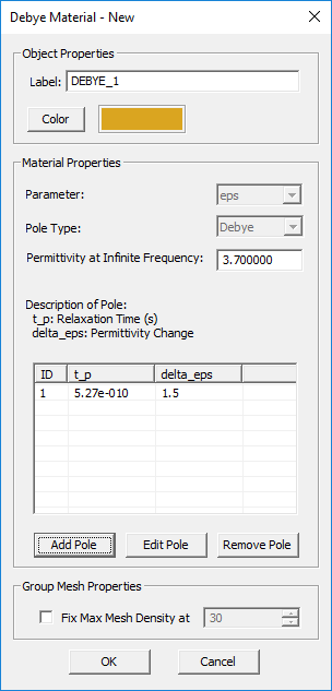
- Right-click on the Dispersive Materials item in the navigation tree.
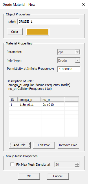
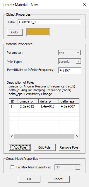
- Select Insert New Debye Material... or Insert New Drude Material... or Insert New Lorentz Material... or Insert New Generalized Metamaterial... or to open up one of the four Dispersive Material dialogs.
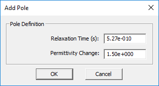
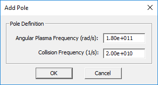
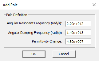
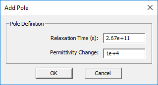
- You have to define each pole of the dispersive material individually. You can add as many poles as you want using the Add Pole button of the dialog.
- Click the OK button of the dialog to return to the project workspace.
NOTES, SPECIAL CASES OR EXCEPTIONS: EM.Tempo currently offers four types of dispersive material:
- Debye Material
- Drude Material (Unmagnetized Plasma)
- Lorentz Material
- Generalized Metamaterial
The FDTD simulation engine uses the Auxiliary Differential Equation (ADE) method to model dispersive materials. EM.Cube allows you to define an arbitrary number of poles for each of the above dispersive material types. Keep in mind that all the objects belonging to the same dispersive material group have the same dispersion properties.
The complex permittivity of a Debye material with N poles is given by:
- [math] \varepsilon (\omega) = \varepsilon_\infty + \sum_{p=1}^N \dfrac{\Delta \varepsilon_p}{1 + j\omega \tau_p}, \quad \Delta \varepsilon_p = \varepsilon_{sp} - \varepsilon_\infty [/math]
where [math]\varepsilon_{\infty}[/math] is the value of the permittivity at infinite frequency, [math]\tau_p[/math] is the relaxation time corresponding to the pth pole having the unit of seconds, and [math]\varepsilon_{sp}[/math] is the value of the static permittivity (at DC) corresponding to the pth pole. [math]\Delta \varepsilon_p = \varepsilon_{sp} - \varepsilon_{\infty}[/math] represents the change in permittivity due to the pth pole.
Unmagnetized plasmas are typically modeled as Drude materials. The complex permittivity of a Drude material with N poles is given by:
- [math] \varepsilon(\omega) = \varepsilon_{\infty} - \sum_{p=1}^N \dfrac{{\omega_p}^2}{\omega^2 - j\omega \nu_p} [/math]
where [math]\omega_p[/math] and [math]\nu_p[/math] are the angular plasma frequency and angular collision frequency corresponding to the pth pole, respectively, and both are expressed in rad/s. For an unmagnetized plasma, [math]\varepsilon_{\infty} = 1[/math].
The complex permittivity of a Lorentz material with N poles is given by:
- [math] \varepsilon(\omega) = \varepsilon_{\infty} - \sum_{p=1}^N \dfrac{\Delta \varepsilon_p {\omega_p}^2}{\omega^2 - 2j\omega \delta_p - {\omega_p}^2}, \quad \Delta \varepsilon_p = \varepsilon_{sp} - \varepsilon_{\infty} [/math]
where [math]\omega _p[/math] and [math]\delta_p[/math] are the angular resonant frequency and angular damping frequency corresponding to the pth pole, respectively, and both are expressed in rad/s. Similar to a Debye material, [math]\Delta \varepsilon_p = \varepsilon_{sp} - \varepsilon_{\infty}[/math] represents the change in permittivity due to the pth pole.
The Debye, Drude and Lorentz dispersive materials are all isotropic dielectric materials having a scalar relative permittivity that varies with the frequency. A generalized metamaterial in EM.Tempo is defined as a uniaxial dispersive material that has three relative permittivities εr,xx, εr,yy, εr,zz and three relative permeabilities μr,xx, μr,yy, and μr,zz. These six quantities can independently be functions of the frequency in general or non-dispersive. Moreover, you can define poles of different kind for each constitutive parameter. The pole type can be Debye, Drude or Lorentz.
PYTHON COMMAND: None
DISPERSIVE MATERIAL PARAMETERS
| Parameter Name | Value Type | Units | Default Value | Notes |
|---|---|---|---|---|
| Locked mesh density | Real Numeric | cells/effective wavelength | 30 | Only if "Lock Mesh" enabled |
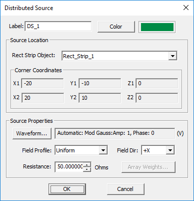
Distributed Source
MODULE: EM.Tempo
FUNCTION: Places a distributed voltage source with a distributed internal resistor over a virtual rectangle strip object that is parallel to one of the three principal planes
TO DEFINE A DISTRIBUTED SOURCE:
- Right-click on the Distributed Sources item in the navigation tree of EM.Tempo.
- Select Insert New Source... to open up the Distributed Source Dialog.
- From the Host drop-down list, select a rectangle strip object. Note that only rectangle strip objects of virtual type and parallel to one of the three principal planes are listed.
- A distributed source has a field profile with three options: uniform, sinusoidal and edge-singular. The default option is uniform.
- The direction of the impressed electric field can be aligned along one of the edges of its host rectangle strip object, either in the positive or negative direction. You can select the desired direction from the Field Dir drop-down list.
- Click the OK button of the dialog to return to the project workspace.
NOTES, SPECIAL CASES OR EXCEPTIONS: The current version of EM.Tempo provides three spatial field profiles for a distributed source:
- Uniform: E = E0
- Sinusoidal: E = E0 cos(πy/w)
- Edge-Singular: E = E0 / √ [ 1-(2y/w)^2 ]
In the above functional forms, E0 is a constant, y is the coordinate along the direction of field variation measured from the center of the rectangular area and w is its total width along the y direction.
PYTHON COMMAND: distributed_src(label,rect_object,field_dir,profile[,magnitude,phase,resistance])
DISTRIBUTED SOURCE PARAMETERS
| Parameter Name | Value Type | Units | Default Value | Notes |
|---|---|---|---|---|
| profile | List: uniform, sinusoidal, edge-singular | V/m | uniform | field distribution profile in the host rectangular region |
| offset | real numeric | project units | half the length of host line object | distance between the source and the start point of the host line object |
| resistance | real numeric | Ohms | 50 | internal impedance of the distributed voltage source |
Embedded Dielectric Object Set
MODULE: EM.Picasso
FUNCTION: Defines an embedded dielectric object set group
TO DEFINE AN EMBEDDED DIELECTRIC SET:
- Right-click on the Embedded Object Sets item in the navigation tree.
- Select Insert New Dielectric Set... to open up the New Dielectric Object Set dialog.
- From the drop-down list labeled Host Layer, select the substrate layer to embed the new object set.
- Enter values for relative permittivity εr and electric conductivity σ in S/m. The default values are εr = 1 and σ = 0, representing an air void.
- Click the OK button of the dialog to return to the project workspace.
PYTHON COMMAND:
pec_via_group(label,host_layer)
EMBEDDED DIELECTRIC SET PARAMETERS
| Parameter Name | Value Type | Units | Default Value | Notes |
|---|---|---|---|---|
| eps (εr) | Real Numeric | - | 1.0 | relative permittivity |
| sigma (σ) | Real Numeric | S/m | 0.0 | electric conductivity |
| Locked mesh density | Real Numeric | cells/effective wavelength | 30 | Only if "Lock Mesh" enabled |
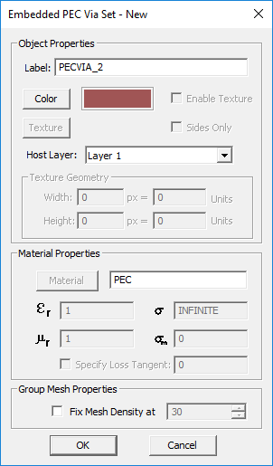
Embedded PEC Via Set
MODULE: EM.Picasso
FUNCTION: Defines an embedded PEC via object set group
TO DEFINE A PEC VIA SET:
- Right-click on the Embedded Object Sets item in the navigation tree.
- Select Insert New PEC Via Set... to open up the New PEC Vias Set Dialog.
- From the drop-down list labeled Host Layer, select the substrate layer to embed the new via set.
- Change the color or texture of the via set if desired.
- Click the OK button of the dialog to return to the project workspace.
PYTHON COMMAND:
pec_via_group(label,host_layer)
EMBEDDED PEC VIA SET PARAMETERS
| Parameter Name | Value Type | Units | Default Value | Notes |
|---|---|---|---|---|
| Locked mesh density | Real Numeric | cells/effective wavelength | 30 | Only if "Lock Mesh" enabled |
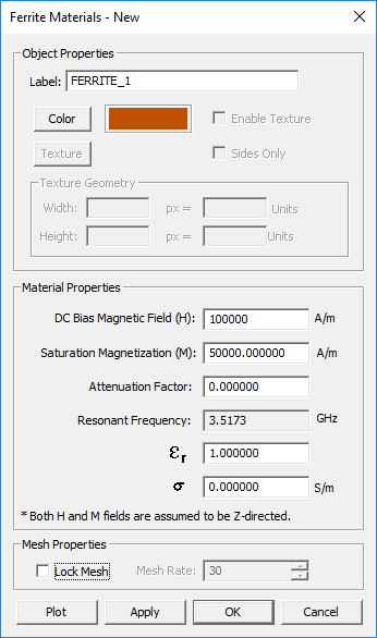
Ferrite Material
MODULE: EM.Tempo
FUNCTION: Defines a ferrite material
TO DEFINE A FERRITE MATERIAL GROUP:
- Right-click on the Gyrotropic Materials item in the navigation tree.
- Select Insert New Ferrite Material... to open up the New Ferrite dialog.
- Enter values for the DC Bias Magnetic Field and Saturation Magnetization.
- If necessary, change the default values of attenuation factor, permittivity and electric conductivity.
- Change the color of the material group if desired.
- Clicking the Plot button generates plots of the components of the permeability tensor over the frequency range of the project.
- Click the OK button of the dialog to return to the project workspace.
PYTHON COMMAND: None
VOXEL DATABASE PARAMETERS
| Parameter Name | Value Type | Units | Default Value | Notes |
|---|---|---|---|---|
| DC Bias Magnetic Field | Real Numeric | A/m | 100000 | Assumed to be Z-directed |
| Saturation Magnetization | Real Numeric | A/m | 50000 | Assumed to be Z-directed |
| Attenuation Factor | Real Numeric | - | 0 | - |
| eps (εr) | Real Numeric | - | 1.0 | relative permittivity |
| sigma (σ) | Real Numeric | S/m | 0.0 | electric conductivity |
| Locked mesh density | Real Numeric | cells/effective wavelength | 30 | Only if "Lock Mesh" enabled |
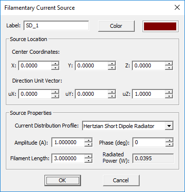
Filamentary Current Source
MODULE: EM.Tempo
FUNCTION: Places a filamentary current source at a specified location in the project workspace
TO DEFINE A FILAMENTARY CURRENT SOURCE:
- Right-click on the Filamentary Current Sources item in the navigation tree.
- Either select Insert New Hertzian Short Dipole Source... or select Insert New Long Wire Current Source... to open up the Filamentary Current Source Dialog.
- By default, the filamentary current source is placed at the origin of coordinates. You can modify the source's center coordinates.
- The "Current Distribution Profile" dropdown list provides four options: Hertzian Short Dipole Radiator, Uniform Long Wire Current, Triangular Long Wire Current and Sinusoidal Long Wire Current. Select the desired type.
- By default, a vertical Z-directed current is defined. You can change the components of the unit vector along the dipole to reorient it along any arbitrary direction. In the case of a long wire current source, it has to be oriented along one of the three principal axes. In other words, only one of uX, uY or uZ components must be one and the other two must be zero.
- You may also modify the current amplitude and phase as well as the filament length.
- Click the OK button of the dialog to return to the project workspace.
NOTES, SPECIAL CASES OR EXCEPTIONS: A filamentary current source with Hertzian short dipole radiator profile is equivalent to Hertzian Short Dipole Source in the other computational modules of EM.Cube.
PYTHON COMMAND: None
SHORT DIPOLE PARAMETERS
| Parameter Name | Value Type | Units | Default Value | Notes |
|---|---|---|---|---|
| x0 | real numeric | project units | 0 | X-coordinate of source location |
| y0 | real numeric | project units | 0 | Y-coordinate of source location |
| z0 | real numeric | project units | 0 | Z-coordinate of source location |
| amplitude | real numeric | Amperes | 1 | amplitude of filamentary current |
| phase | real numeric | degrees | 0 | phase of filamentary current |
| length | real numeric | project units | 3 | filament length |
| uX | real numeric | - | 0 | X-component of unit direction vector |
| uY | real numeric | - | 0 | Y-component of unit direction vector |
| uZ | real numeric | - | 1 | Z-component of unit direction vector |
Fixed-Potential PEC
MODULE: EM.Ferma
FUNCTION: Defines an equi-potential perfect electric conductor object group with a specified voltage
TO DEFINE A FIXED-POTENTIAL PEC GROUP:
- Right-click on the Fixed-Potential PEC Objects item in the navigation tree.
- Select Insert New Fixed-Potential PEC... to open up the Fixed-Potential PEC dialog.
- Besides the color and texture properties, you have to enter a value for the fixed Voltage in Volts. The default voltage is 0V.
- Click the OK button of the dialog to return to the project workspace.
PYTHON COMMAND: pec_voltage_group(label,voltage)
FIXED-POTENTIAL PEC PARAMETERS
| Parameter Name | Value Type | Units | Default Value | Notes |
|---|---|---|---|---|
| voltage | Real Numeric | Volts | 0 | - |
| Locked mesh density | Real Numeric | cells/effective wavelength | 30 | Only if "Lock Mesh" enabled |
Fixed-Temperature PTC
MODULE: EM.Ferma
FUNCTION: Defines an iso-thermal perfect thermal conductor object group with a specified temperature
TO DEFINE A FIXED-TEMPERATURE PTC GROUP:
- Right-click on the Fixed-Temperature PTC Objects item in the navigation tree.
- Select Insert New Fixed-Potential PEC/PTC... to open up the Fixed-Temperature PTC dialog.
- Besides the color and texture properties, you have to enter a value for the fixed Temperature in degrees C. The default voltage is 0°C.
- Click the OK button of the dialog to return to the project workspace.
PYTHON COMMAND: pec_voltage_group(label,voltage)
FIXED-TEMPERATURE PTC PARAMETERS
| Parameter Name | Value Type | Units | Default Value | Notes |
|---|---|---|---|---|
| temperature | Real Numeric | Deg C | 0 | - |
| Locked mesh density | Real Numeric | cells/effective wavelength | 30 | Only if "Lock Mesh" enabled |
Gaussian Beam
MODULE: EM.Tempo
FUNCTION: Defines a focused Gaussian beam source with specified incidence angles, polarization, beam focus point and beam radius
TO DEFINE A GAUSSIAN BEAM:
- Right-click on the Plane Waves item in the navigation tree.
- Select Insert New Source... to open up the Plane Wave Dialog.
- By default, a TMz-polarized plane wave source is defined with normal incidence along the negative Z-axis.
- You can change the Polarization type and incident Theta and Phi angles in the spherical coordinate system.
- Click the OK button of the dialog to return to the project workspace.
NOTES, SPECIAL CASES OR EXCEPTIONS: Unlike plane waves, a Gaussian beam is a localized field. By default, the dominant fundamental Hermite-Gauss mode H00 is assumed. You can define a higher-order Hermite-Gauss mode by assigning nonzero values for the modal indices p and q.
| |
The beam radius has to be at least λ0/π; otherwise, strong fields appear outside the excitation box. |
PYTHON COMMAND: gauss_beam(label,theta,phi,polarization,focus_x,focus_y,focus_z,radius,p_mode,q_mode)
GAUSSIAN BEAM PARAMETERS
| Parameter Name | Value Type | Units | Default Value | Notes |
|---|---|---|---|---|
| polarization | List: TMz, TEz, Custom Linear | - | TMz | select one of the linear or circular polarization types |
| theta | real numeric | degrees | 180 | incident elevation angle |
| phi | real numeric | degrees | 0 | incident azimuth angle |
| focus_x | real numeric | project units | 0 | X-coordinate of beam focus point |
| focus_y | real numeric | project units | 0 | Y-coordinate of beam focus point |
| focus_z | real numeric | project units | 0 | Z-coordinate of beam focus point |
| radius | real numeric | project units | 10 | beam waist radius |
| p | integer numeric | - | 0 | first index of Hermite-Gauss mode |
| q | integer numeric | - | 0 | second index of Hermite-Gauss mode |
Gyrotropic Material
MODULE: EM.Tempo
FUNCTION: Defines a gyrotropic material (either a ferrite or a magnetoplasma)
TO DEFINE A GYROTROPIC MATERIAL GROUP:
- Right-click on the Gyrotropic Materials item in the navigation tree.
- Select either Insert New Ferrite Material... or Insert New Magnetoplasma... to open up the New Ferrite dialog or New Magneoplasma dialog, respectively.
- For a ferrite material, follow the procedure at Ferrite Material.
- For a magnetoplasma material, follow the procedure at Magnetoplasma Material.
- Change the color of the material group if desired.
- Click the OK button of the dialog to close it.
NOTES, SPECIAL CASES OR EXCEPTIONS: In the case of a magnetoplasma, the user has two options, either to specify the DC magnetic field or the angular cyclotron frequency. Once either of the two parameter is specified, the value of the other parameter is computed and displayed.
PYTHON COMMAND: None
FERRITE MATERIAL PARAMETERS
| Parameter Name | Value Type | Units | Default Value | Notes |
|---|---|---|---|---|
| DC bias magnetic field | Real Numeric | A/m | 105 | assumed to be Z-directed |
| saturation magnetization | Real Numeric | A/m | 5×10⁴ | assumed to be Z-directed |
| attenuation factor | Real Numeric | - | 0 | must be between 0 and 1 |
| relative permittivity | Real Numeric | - | 1 | - |
| electric conductivity | Real Numeric | S/m | 0 | - |
| Locked mesh density | Real Numeric | cells/effective wavelength | 30 | Only if "Lock Mesh" enabled |
MAGNETOPLASMA MATERIAL PARAMETERS
| Parameter Name | Value Type | Units | Default Value | Notes |
|---|---|---|---|---|
| angular plasma frequency | Real Numeric | rad/s | 3.14×10⁷ | - |
| collision frequency | Real Numeric | 1/s | 105 | - |
| DC bias magnetic field | Real Numeric | A/m | 105 | assumed to be Z-directed |
| angular cyclotron frequency | Real Numeric | rad/s | 8837887.024 | must be specified if the DC magnetic field check box is unchecked |
| Locked mesh density | Real Numeric | cells/effective wavelength | 30 | Only if "Lock Mesh" enabled |
Hertzian Short Dipole Source
MODULE: EM.Tempo, EM.Terrano, EM.Illumina, EM.Picasso, EM.Libera
FUNCTION: Places a short dipole radiator at a specified location in the project workspace
TO DEFINE A SHORT DIPOLE SOURCE:
- Right-click on the Hertzian Short Dipoles item in the navigation tree.
- Select Insert New Source... to open up the Short Dipole Dialog.
- By default, the short dipole radiator is placed at the origin of coordinates. You can modify the source coordinates.
- By default, a vertical Z-directed short dipole radiator is defined. You can change the components of the unit vector along the dipole to reorient it along any arbitrary direction.
- You may also modify the current strength and length of the Hertzian dipole.
- Click the OK button of the dialog to return to the project workspace.
NOTES, SPECIAL CASES OR EXCEPTIONS: A Hertzian dipole is the simplest type of radiator, which consists of a short current element of length Δl, aligned along a unit vector û and carrying a current of I Amperes. The product IΔl is often called the dipole moment and gives a measure of the radiator's strength. A short vertical dipole in the free space generates an azimuth-symmetric, almost omni-directional, far field. The fields radiated by a short Hertzian dipole in a free-space background medium are given by:
- [math] \mathbf{ E^{inc}(r) } = - jk_0 Z_0 (I\Delta l) \left\{ \left[ 1 - \frac{j}{k_0 R} - \frac{1}{(k_0 R)^2} \right] \mathbf{\hat{u}} - \left[ 1 - \frac{3j}{k_0 R} - \frac{3}{(k_0 R)^2} \right] \mathbf{ (\hat{R} \cdot \hat{u}) } \right\} \frac{e^{-jk_0 R}}{4\pi R} [/math]
- [math] \mathbf{ H^{inc}(r) } = - jk_0 (I\Delta l) \left[ 1-\frac{j}{k_0 R} \right] \mathbf{ (\hat{R} \times \hat{u} ) } \frac{e^{-jk_0 R}}{4\pi R} [/math]
where [math] R=|r-r'| \text{, } k_0 = \frac{2\pi}{\lambda_0} \text{ and } Z_0 = 1/Y_0 = \eta_0 [/math], λ0 is the operating wavelength, [math]\mathbf{\hat{u}}[/math] is the unit vector along the dipole, and r0 = (x0, y0, z0) is the position vector of the dipole source.
The radiation resistance of the short dipole is given by:
- [math] R_r = 80\pi^2 \left( \frac{\Delta l}{\lambda_0} \right)^2 [/math]
The radiated power of the short dipole carrying a current I is displayed in the source dialog and is computed as:
- [math] P_{rad} = \frac{1}{2} R_r |I_0|^2 = 40\pi^2 |I|^2 \left( \frac{\Delta l}{\lambda_0} \right)^2 [/math]
The radiated fields of a short dipole above a layered planar background structure are greatly altered by the presence of the substrate layers. The electric and magnetic fields radiated by a short dipole in the presence of a layered background structure are indeed the dyadic Green's functions of that structure:
- [math] \mathbf{E^{inc}(r)} = \int_{\Delta_L} \mathbf{\overline{\overline{G_{EJ}}}(r|r')} \cdot (I\Delta l \mathbf{\hat{u}}) \, dl' [/math]
- [math] \mathbf{H^{inc}(r)} = \int_{\Delta_L} \mathbf{\overline{\overline{G_{HJ}}}(r|r')} \cdot (I\Delta l \mathbf{\hat{u}}) \, dl' [/math]
PYTHON COMMAND: short_dipole(label,x0,y0,z0,length,uX,uY,uZ,amplitude,phase)
SHORT DIPOLE PARAMETERS
| Parameter Name | Value Type | Units | Default Value | Notes |
|---|---|---|---|---|
| x0 | real numeric | project units | 0 | X-coordinate of source location |
| y0 | real numeric | project units | 0 | Y-coordinate of source location |
| z0 | real numeric | project units | 0 | Z-coordinate of source location |
| amplitude | real numeric | Amperes | 1 | amplitude of dipole current |
| phase | real numeric | degrees | 0 | phase of dipole current |
| length | real numeric | project units | 3 | dipole length |
| uX | real numeric | - | 0 | X-component of unit direction vector |
| uY | real numeric | - | 0 | Y-component of unit direction vector |
| uZ | real numeric | - | 1 | Z-component of unit direction vector |
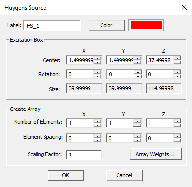
Huygens Source
MODULE: EM.Tempo, EM.Terrano, EM.Illumina, EM.Picasso, EM.Libera
FUNCTION: Defines an equivalent Huygens source based on a specified Huygens surface data file
TO DEFINE A HUYGENS SOURCE:
- Right-click on the Huygens Sources item in the navigation tree.
- Select Import New Source... to open up Window's Open Dialog. The file extension is automatically set to ".HUY".
- Browse your folders to find the desired Huygens surface data file. Select it and click the Open button of the dialog.
- A Huygens source box appears in the project workspace. You can open the property dialog of the Huygens source and change its location and orientation.
PYTHON COMMAND: huygens_src(label,filename,[set_lcs,x0,y0,z0,x_rot,y_rot,z_rot])
HUYGENS SOURCE PARAMETERS
| Parameter Name | Value Type | Units | Default Value | Notes |
|---|---|---|---|---|
| x0 | real numeric | project units | - | X-coordinate of centroid of the Huygens source box |
| y0 | real numeric | project units | - | Y-coordinate of centroid of the Huygens source box |
| z0 | real numeric | project units | - | Z-coordinate of centroid of the Huygens source box |
| rot_x | real numeric | degrees | 0 | rotation angle of the Huygens source box about the local X-axis |
| rot_y | real numeric | degrees | 0 | rotation angle of the Huygens source box about the local Y-axis |
| rot_z | real numeric | degrees | 0 | rotation angle of the Huygens source box about the local Z-axis |
Impedance/Dielectric Surface
MODULE: EM.Illumina
FUNCTION: Defines an impedance surface object group
TO DEFINE AN IMPEDANCE/DIELECTRIC SURFACE GROUP:
- Right-click on the Impedance/Dielectric Surfaces item in the navigation tree.
- Select Insert New Impedance or dielectric Surface... to open up the impedance Surface dialog.
- Besides the color and texture properties, you have to enter values for the real and imaginary parts of Surface Impedance. The default values are 0 + j0 Ω, representing a PEC surface.
- Click the OK button of the dialog to return to the project workspace.
NOTES, SPECIAL CASES OR EXCEPTIONS: An impedance surface is a surface on which the tangential electric and magnetic fields are governed by the surface impedance boundary condition (SIBC):
- [math] \mathbf{\hat{n}} \times \mathbf{\hat{n}} \times \mathbf{E} = -Z_s \mathbf{J_s} = -Z_s \mathbf{\hat{n}} \times \mathbf{H} [/math]
where [math]Z_s[/math] is the surface impedance in Ohms and [math]\mathbf{\hat{n}}[/math] is the unit outward normal on the given surface.
PYTHON COMMAND: impedance_surface_group(label,z_real,z_imag)
IMPEDANCE SURFACE PARAMETERS
| Parameter Name | Value Type | Units | Default Value | Notes |
|---|---|---|---|---|
| resistance | Real Numeric | Ohm | 0.0 | real part of surface impedance |
| reactance | Real Numeric | Ohm | 0.0 | imaginary part of surface impedance |
| Locked mesh density | Real Numeric | cells/effective wavelength | 30 | Only if "Lock Mesh" enabled |
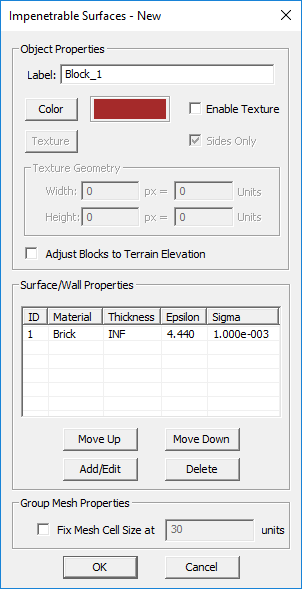
Impenetrable Surface
MODULE: EM.Terrano
FUNCTION: Defines an impenetrable surface block group
TO DEFINE AN IMPENETRABLE SURFACE GROUP:
- Right-click on the Impenetrable Surfaces item in the navigation tree.
- Select Insert New Block... to open up the Impenetrable Surface dialog.
- In the material table, the default setting shows Brick with a relative permittivity of εr = 4.44 and an electric conductivity of σ = 0.001S/m.
- You can change the default material composition by selecting and highlighting it in the table and clicking the Add/Edit button of the dialog.
- In the Material Layer Properties dialog, either enter new values for εr and σ or click the Material button of this dialog to open EM.Cube's Materials List and select one of its entries.
- You can add several layers to your impenetrable surface composition. In that case, you need to define a thickness for each layer. The bottommost layer always has an infinite thickness representing an unbounded half-space medium as seen by an incident ray.
- After you complete the definition of all layers, click the OK button of the dialog to return to the project workspace.
PYTHON COMMAND: impenetrable_surface_group(label,epsilon,sigma[,rr,gg,bb])
IMPENETRABLE SURFACE PARAMETERS
| Parameter Name | Value Type | Units | Default Value | Notes |
|---|---|---|---|---|
| epsilon | Real Numeric | - | 4.44 | relative permittivity |
| sigma | Real Numeric | S/m | 1e-3 | electric conductivity |
| Locked mesh density | Real Numeric | cells/effective wavelength | 30 | Only if "Lock Mesh" enabled |
Inductor
MODULE: EM.Tempo
FUNCTION: Places an inductor at a specified point on a PEC line object that is parallel to one of the three principal axes
TO DEFINE A INDUCTOR:
- Right-click on the Lumped Devices item in the navigation tree.
- Select Insert New Source... to open up the Lumped Device Dialog.
- From the Host drop-down list, select a line object. Note that only line parallel to one of the three principal axes are listed.
- From the Type drop-down list, select Inductor.
- By default, the lumped device is placed at the midpoint of the host line object. You can modify the Offset parameter, which is measured from the start point of the line and is always positive.
- Enter a value for Inductance in nH. The default inductance is 1nH.
- Click the OK button of the dialog to return to the project workspace.
PYTHON COMMAND: inductor(label,line_object,offset,inductance_nH)
LUMPED INDUCTOR PARAMETERS
| Parameter Name | Value Type | Units | Default Value | Notes |
|---|---|---|---|---|
| offset | real numeric | project units | half the length of host line object | distance between the device and the start point of the host line object |
| inductance | real numeric | nH | 1 | - |
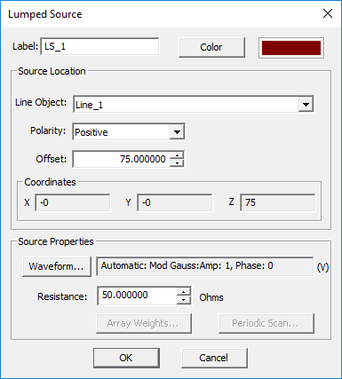
Lumped Source
MODULE: EM.Tempo
FUNCTION: Places an ideal voltage source with a series internal resistor at a specified point on a PEC or thin wire line object that is parallel to one of the three principal axes
TO DEFINE A LUMPED SOURCE:
- Right-click on the Lumped Sources item in the navigation tree.
- Select Insert New Source... to open up the Lumped Source Dialog.
- From the Host drop-down list, select a line object. Note that only line parallel to one of the three principal axes are listed.
- By default, the lumped source is placed at the midpoint of the host line object. You can modify the Offset parameter, which is measured from the start point of the line and is always positive.
- Click the OK button of the dialog to return to the project workspace.
PYTHON COMMAND: lumped_src(label,line_object,offset,polarity[,amplitude,phase,resistance])
LUMPED SOURCE PARAMETERS
| Parameter Name | Value Type | Units | Default Value | Notes |
|---|---|---|---|---|
| polarity | List: pos, neg | - | - | polarity of the voltage source |
| offset | real numeric | project units | half the length of host line object | distance between the source and the start point of the host line object |
| resistance | real numeric | Ohms | 50 | internal impedance of voltage source at the gap |
Magnetoplasma Material
MODULE: EM.Tempo
FUNCTION: Defines a magnetoplasma material
TO DEFINE A FERRITE MATERIAL GROUP:
- Right-click on the Gyrotropic Materials item in the navigation tree.
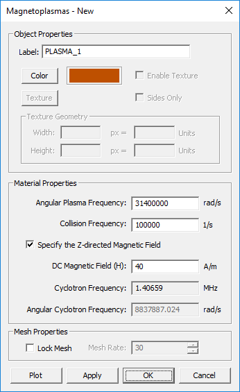
- Select Insert New Magnetoplasma... to open up the New Magnetoplasma dialog.
- Enter values for the Angular Plasma Frequency and Collision Frequency.
- The box labeled "Specify the Z-directed DC Magnetic Field" is checked by default. In that case, you need to enter a value for the DC magnetic field.
- If you uncheck the magnetic field box, then you need to enter a value for Angular Cyclotron Frequency.
- Change the color of the material group if desired.
- Clicking the Plot button generates plots of the components of the permittivity tensor over the frequency range of the project.
- Click the OK button of the dialog to return to the project workspace.
PYTHON COMMAND: None
VOXEL DATABASE PARAMETERS
| Parameter Name | Value Type | Units | Default Value | Notes |
|---|---|---|---|---|
| Angular Plasma Frequency | Real Numeric | rad/s | 31400000 | - |
| Collision Frequency | Real Numeric | 1/s | 100000 | - |
| DC Magnetic Field | Real Numeric | A/m | 40 | Assumed to be Z-directed |
| Angular Cyclotron Frequency | Real Numeric | rad/s | 8837887.024 | Disabled when specifying the DC magnetic field |
| Locked mesh density | Real Numeric | cells/effective wavelength | 30 | Only if "Lock Mesh" enabled |
Microstrip Port
MODULE: EM.Tempo
FUNCTION: Places a special distributed source of a specified height underneath one of the edges of a PEC rectangle strip object that is parallel to one of the three principal planes
TO DEFINE A MICROSTRIP PORT:
- Right-click on the Microstrip Ports item in the navigation tree of EM.Tempo.
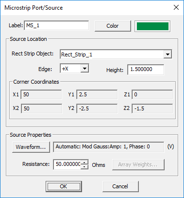
- Select Insert New Source... to open up the Microstrip Port Dialog.
- From the Host drop-down list, select a rectangle strip object. Note that only PEC rectangle strip objects parallel to one of the three principal planes are listed.
- You have to specify the height of the microstrip port, which is the same as the height of the microstrip's substrate.
- A microstrip port can be placed at one of the four edges of the host rectangle strip. You can select the desired location from the Edge drop-down list.
- Click the OK button of the dialog to return to the project workspace.
PYTHON COMMAND: microstrip_src(label,rect_object,height,edge[,magnitude,phase,resistance])
MICROSTRIP PORT PARAMETERS
| Parameter Name | Value Type | Units | Default Value | Notes |
|---|---|---|---|---|
| height | real numeric | project units | 1.5 | microstrip's substrate height |
| resistance | real numeric | Ohms | 50 | internal impedance of the distributed voltage source |
Parallel RC Device
MODULE: EM.Tempo
FUNCTION: Places a collocated parallel combination of a resistor and a capacitor at a specified point on a PEC line object that is parallel to one of the three principal axes
TO DEFINE A SERIES RL DEVICE:
- Right-click on the Lumped Devices item in the navigation tree.
- Select Insert New Source... to open up the Lumped Device Dialog.
- From the Host drop-down list, select a line object. Note that only lines parallel to one of the three principal axes are listed.
- From the Type drop-down list, select Parallel RC.
- By default, the lumped device is placed at the midpoint of the host line object. You can modify the Offset parameter, which is measured from the start point of the line and is always positive.
- Enter a value for Resistance in Ohms and a value for Capacitance in pF. The default values are 100Ω and 1pF, respectively.
- Click the OK button of the dialog to return to the project workspace.
PYTHON COMMAND: None
LUMPED PARALLEL RC DEVICE PARAMETERS
| Parameter Name | Value Type | Units | Default Value | Notes |
|---|---|---|---|---|
| offset | real numeric | project units | half the length of host line object | distance between the device and the start point of the host line object |
| resistance | real numeric | Ohms | 100 | - |
| capacitance | real numeric | pF | 1 | - |
Penetrable Surface
MODULE: EM.Terrano
FUNCTION: Defines a penetrable surface (thin wall) block group of a specified thickness
TO DEFINE AN PENETRABLE SURFACE GROUP:
- Right-click on the Penetrable Surfaces item in the navigation tree.
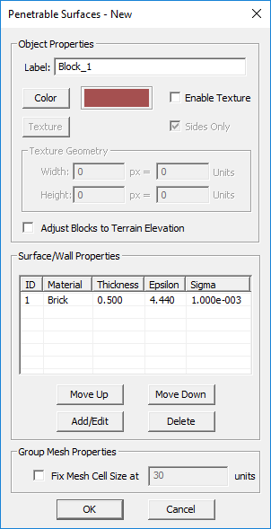
- Select Insert New Block... to open up the Penetrable Surface dialog.
- In the material table, the default setting shows Brick with a relative permittivity of εr = 4.44, an electric conductivity of σ = 0.001S/m and a thickness of 0.5 project units.
- You can change the default material composition by selecting and highlighting it in the table and clicking the Add/Edit button of the dialog.
- In the Material Layer Properties dialog, either enter new values for εr and σ or click the Material button of this dialog to open EM.Cube's Materials List and select one of its entries. You can also change the Wall Thickness from this dialog.
- You can add several layers to your penetrable wall composition. An incident ray first penetrates the topmost layer and finally exits the bottommost layer.
- After you complete the definition of all layers, click the OK button of the dialog to return to the project workspace.
PYTHON COMMAND: penetrable_surface_group(label,epsilon,sigma,thickness[,rr,gg,bb])
PENETRABLE SURFACE PARAMETERS
| Parameter Name | Value Type | Units | Default Value | Notes |
|---|---|---|---|---|
| epsilon | Real Numeric | - | 4.44 | relative permittivity |
| sigma | Real Numeric | S/m | 1e-3 | electric conductivity |
| thickness | Real Numeric | project units | 0.5 | finite thickness of thin walls |
| Locked mesh density | Real Numeric | cells/effective wavelength | 30 | Only if "Lock Mesh" enabled |
Penetrable Volume
MODULE: EM.Terrano
FUNCTION: Defines a penetrable volume block group
TO DEFINE AN PENETRABLE VOLUME GROUP:
- Right-click on the Penetrable Volumes item in the navigation tree.
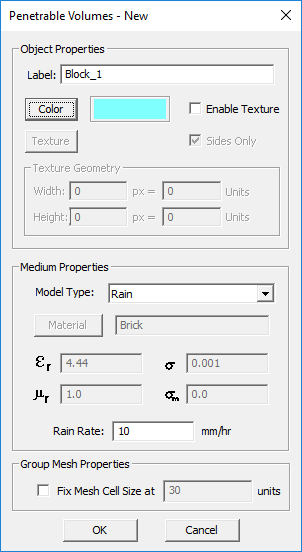
- Select Insert New Block... to open up the Penetrable Volume dialog.
- From the Interface drop-down dialog, choose one of the four options: Standard Material, Rain, Fog, Vegetation.
- The default interface type is the standard material Brick with a relative permittivity of εr = 4.44, an electric conductivity of σ = 0.001S/m.
- You can change the default material composition by entering new values for εr and σ. Or click the Material button of this dialog to open EM.Cube's Materials List and select one of its entries.
- If you choose the Rain option, you have to enter a value for Rain Rate in mm/hr.
- If you choose the Fog option, you have to enter a value for Fog Density in g/m^3.
- If you choose the Vegetation option, Weissberger's model will be used and there is no parameter to set.
- After you complete the definition of all layers, click the OK button of the dialog to return to the project workspace.
NOTES, SPECIAL CASES OR EXCEPTIONS: Inside a penetrable volumes, the rays travel through a non-air medium. As a result, they experience different phase velocities and possibly additional losses. Therefore, the attenuation and propagation constants of the material medium are used for wave computations:
- [math] \gamma = \alpha + j\beta = \alpha + j\frac{\omega}{c}\sqrt{\epsilon_r} [/math]
where α and β are the attenuation and propagation constants in Neper/m and radian/m, respectively, ω = 2*πf, εr is the relative permittivity of the medium and f the operational frequency.
There are four types of penetrable volumes:
- Standard material
- Rain
- Fog
- Vegetation
Standard material blocks reflect, transmit and diffract impinging rays. The ray reflection and edge diffraction mechanisms are identical to the cases of impenetrable or penetrable surfaces with the same material properties. The transmitted rays, however, travel in the material medium until they exit the other side of the penetrable volume object. This is different than the case of penetrable surfaces, where the transmitter ray is assumed to travel the very short thickness of a wall before entering the free space again, and the specular points of the entering and exiting rays are taken to be the same.
Of the above list, rain, fog and vegetation media only attenuate the incoming ray and do not generate reflected or diffracted rays. A rain medium is characterized by the Rain Rate expressed in mm/hr, and a fog medium is characterized by the Fog Density expressed in gr/m3. EM.Terrano uses Weissberger's model for the calculation of attenuation due to propagation in a vegetation medium. This model is only applicable when there is foliage obstruction (blockage by dense, dry and leafy trees) in a line-of-sight link. Weissberger's model is valid in the frequency range from 230MHz to 95GHz and provides accurate results for foliage depths up to 400m. It expressed the propagation loss as
- [math] L = \left\{ \begin{array}{lr} 0.45 f^{0.284}d & d\lt14\text{m} \\ 1.33 f^{0.284}d^{0.588} & 14\text{m} \le d \le 400\text{m} \end{array} \right. [/math]
where L is the total loss in dB, d is the depth of the foliage and f is the operational frequency in GHz.
PYTHON COMMAND: penetrable_volume_group(label,epsilon,sigma[,rr,gg,bb])
PENETRABLE VOLUME PARAMETERS
| Parameter Name | Value Type | Units | Default Value | Notes |
|---|---|---|---|---|
| eps | Real Numeric | - | 4.44 | relative permittivity |
| sigma | Real Numeric | S/m | 1e-3 | electric conductivity |
| Locked mesh density | Real Numeric | cells/effective wavelength | 30 | Only if "Lock Mesh" enabled |
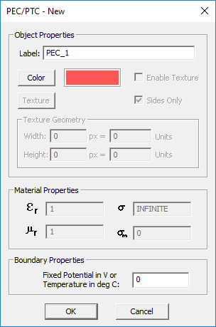
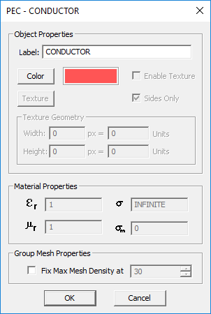
Perfect Electric Conductor (PEC)
MODULE: EM.Tempo, EM.Illumina, EM.Ferma, EM.Picasso, EM.Libera
FUNCTION: Defines a perfect electric conductor object group
TO DEFINE A PEC GROUP:
- Right-click on the PEC Objects or PEC Traces item in the navigation tree.
- Select Insert New PEC... to open up the New PEC Dialog.
- The only properties of a PEC group you can modify is its color and texture.
- Click the OK button of the dialog to return to the project workspace.
PYTHON COMMAND: pec_group(label)
PEC PARAMETERS
| Parameter Name | Value Type | Units | Default Value | Notes |
|---|---|---|---|---|
| Locked mesh density | Real Numeric | cells/effective wavelength | 30 | Only if "Lock Mesh" enabled |
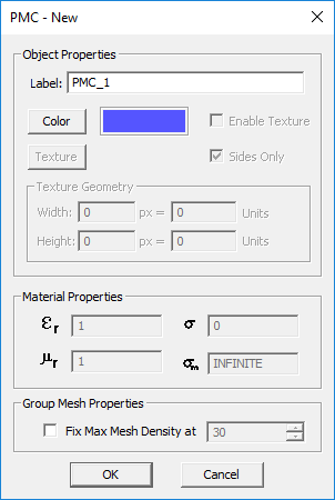
Perfect Magnetic Conductor (PMC)
MODULE: EM.Tempo, EM.Illumina
FUNCTION: Defines a perfect magnetic conductor object group
TO DEFINE A PMC GROUP:
- Right-click on the PMC Planes or PMC Surfaces item in the navigation tree.
- Select Insert New PMC... to open up the New PMC dialog.
- The only properties of a PMC group you can modify is its color and texture.
- Click the OK button of the dialog to return to the project workspace.
PYTHON COMMAND: pmc_group(label)
PMC PARAMETERS
| Parameter Name | Value Type | Units | Default Value | Notes |
|---|---|---|---|---|
| Locked mesh density | Real Numeric | cells/effective wavelength | 30 | Only if "Lock Mesh" enabled |
Permanent Magnet
MODULE: EM.Ferma
FUNCTION: Defines a permanent magnet group with a specified magnetization vector
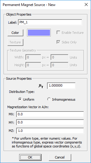
TO DEFINE A PERMANENT MAGNET GROUP:
- Right-click on the Permanent Magnets item in the navigation tree.
- Select Insert New Permanent Magnet... to open up the Permanent Magnet Source dialog.
- Enter a value for relative permeability μr, which has a default value of 1.
- You have two options for Magnetization to choose from: Uniform and Inhomogeneous.
- If you choose the uniform option, you have to enter three numeric values for the three components of the magnetization vector Mx, My and Mz in A/m.
- If you choose the inhomogeneous option, you have to enter three expressions for the three components of the magnetization vector Mx, My and Mz in the global (x,y,z) coordinates.
- Click the OK button of the dialog to return to the project workspace.
NOTES, SPECIAL CASES OR EXCEPTIONS: A permanent magnet is typically a ferromagnetic material with a fixed intrinsic magnetization vector. As a result, it can be used as a source in an magnetostatic problem. When a permeable material has a permanent magnetization, the following relationship holds:
[math] \mathbf{B(r)} = {\mu} (\mathbf{H(r)} + \mathbf{M(r)} ) [/math]
where M(r) is the magnetization vector. In SI units system, the magnetic field H and magnetization M both have the same units of A/m.
It can be shown that for magnetostatic analysis, the effect of the permanent magnetization can be modeled as an equivalent volume current source:
[math] \mathbf{J_{eq}(r)} = \nabla \times \mathbf{M(r)} [/math]
If the magnetization vector is uniform and constant inside the volume, then its curl is zero everywhere inside the volume except on its boundary surface. In this case, the permanent magnetic can be effectively modeled by an equivalent surface current density on the surface of the permanent magnetic object:
[math] \mathbf{J_{s,eq}(r)} = \mathbf{M(r)} \times \hat{\mathbf{n}} [/math]
where [math] \hat{\mathbf{n}} [/math] is the unit outward normal vector at the surface of the permanent magnet object. Note that the volume of the permanent magnet still acts as a permeable material in the magnetostatic analysis.
PYTHON COMMAND: magnet_group(label,mu,Mx,My,Mz)
PERMANENT MAGNET PARAMETERS
| Parameter Name | Value Type | Units | Default Value | Notes |
|---|---|---|---|---|
| mu (μr) | Real Numeric | - | 1.0 | relative permeability |
| Mx | Real Numeric | A/m | 0.0 | X-component of magnetization vector |
| My | Real Numeric | A/m | 0.0 | Y-component of magnetization vector |
| Mz | Real Numeric | A/m | 1.0 | Z-component of magnetization vector |
Plane Wave
MODULE: EM.Tempo, EM.Illumina, EM.Picasso, EM.Libera
FUNCTION: Defines a plane wave source with specified incidence angles and polarization
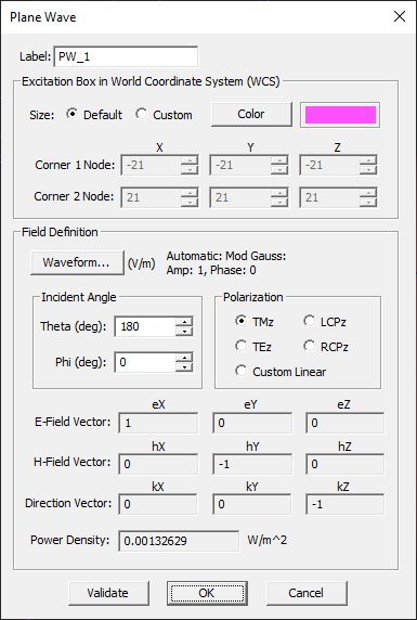
TO DEFINE A PLANE WAVE:
- Right-click on the Plane Waves item in the navigation tree.
- Select Insert New Source... to open up the Plane Wave Dialog.
- By default, a TMz-polarized plane wave source is defined with normal incidence along the negative Z-axis.
- You can change the Polarization type and incident Theta and Phi angles in the spherical coordinate system.
- Click the OK button of the dialog to return to the project workspace.
NOTES, SPECIAL CASES OR EXCEPTIONS: In the case of a free-space background medium, the incident electric and magnetic fields of the plane wave source are given by:
- [math] \mathbf{E^{inc}(r)} = E_0 \mathbf{\hat{e}} e^{ -jk_0 \mathbf{\hat{k}\cdot r} } [/math]
- [math] \mathbf{H^{inc}(r)} = \mathbf{\hat{k} \times \hat{e}} \frac{E_0}{\eta_0} e^{-jk_0 \mathbf{\hat{k} \cdot r} } [/math]
where [math]\eta_0 = 120\pi[/math] is the characteristic impedance of the free space, [math]\mathbf{\hat{k}}[/math] is the unit propagation vector of the incident plane wave, and [math]\mathbf{\hat{e}}[/math] is the polarization vector corresponding to the electric field of that wave.
In EM.Picasso, your plane wave source is placed above a multilayer substrate structure. In that case, the incident plane wave bounces off the layered background structure and part of it also penetrates the substrate layers. The total incident field that is used to calculate the excitation vector is a superposition of the incident, reflected and transmitted plane waves at various regions of your planar structure:
- [math] \mathbf{E^{inc}(r)} = E_0 (\mathbf{\hat{e}_1} e^{ -jk_0 \mathbf{\hat{k}_1\cdot r} } + R \mathbf{\hat{e}_2} e^{ -jk_0 \mathbf{\hat{k}_2\cdot r} } ) [/math]
- [math] \mathbf{H^{inc}(r)} = \frac{E_0}{\eta_0} ( \mathbf{\hat{k}_1 \times \hat{e}_1} e^{-jk_0 \mathbf{\hat{k}_1 \cdot r} } + R \mathbf{\hat{k}_2 \times \hat{e}_2} e^{-jk_0 \mathbf{\hat{k}_2\cdot r} } ) [/math]
where [math]\mathbf{\hat{k}_1}[/math] and [math]\mathbf{\hat{k}_2}[/math] are the unit propagation vectors of the incident plane wave and the wave reflected off the topmost substrate layer, respectively, and [math]\mathbf{\hat{e}_1}[/math] and [math]\mathbf{\hat{e}_2}[/math] are the polarization vectors corresponding to the electric field of those waves. R is the reflection coefficient at the interface between the top half-space and the topmost substrate layer and has different values for the TM and TE polarizations.
PYTHON COMMAND: planewave(label,theta,phi,polarization)
PLANE WAVE PARAMETERS
| Parameter Name | Value Type | Units | Default Value | Notes |
|---|---|---|---|---|
| polarization | List: TMz, TEz, LCPz, RCPz, Custom Linear | - | TMz | select one of the linear or circular polarization types |
| theta | real numeric | degrees | 180 | incident elevation angle |
| phi | real numeric | degrees | 0 | incident azimuth angle |
Point Radiator Set
MODULE: EM.Terrano
FUNCTION: Defines a base location set group to be associated with a transmitter or receiver set
TO DEFINE A BASE LOCATION SET GROUP:
- Right-click on the Base Locataions item in the navigation tree.
- Select Insert New Point Set... to open up the base Location Set dialog.
- The only property of a base location set is its color, which you can change from this dialog.
- Click the OK button of the dialog to return to the project workspace.
- By default, the transmitter set is assumed to be made up of vertical half-wave radiators.
- You may also force the transmitters to adjust their Z-coordinates based on the underlying terrain surface.
- Click the OK button of the dialog to return to the project workspace. The new round symbols appear representing the transmitter set.
- You can open the property dialog of the transmitter set and change the radiator type to User Defined Antenna. In that case, click the Import Pattern button of the dialog to set the file path for a far-field radiation pattern data file of ".RAD" type. You can also additionally rotate the imported radiation pattern about its local X-, Y- and Z-axes.
- An imported radiation pattern file typically contains a total radiated power parameter at its file header. By default, this value is overridden and the Custom Power check box is checked. A default total power of 1W is assigned to each transmitter, which you can change to any arbitrary value. Or you may uncheck Custom Power to use the imported value of the total radiated power.
PYTHON COMMAND radiator_custom_group(label,pattern_file,rot_x,rot_y,rot_z,rr,gg,bb)
POINT RADIATOR SET PARAMETERS:
| Parameter Name | Value Type | Units | Default Value | Notes |
|---|---|---|---|---|
| radiator type | options: vertical half-wave dipole, user define antenna | - | vertical half-wave dipole | - |
| pattern file | file path | - | Models\DPL_STD.RAD | imported far-field radiation pattern data file with a ".RAD" file extension for the case of user defined antenna |
| rot_x | real numeric | degrees | 0 | additional rotation angle of the imported radiation pattern about the local X-axis |
| rot_y | real numeric | degrees | 0 | additional rotation angle of the imported radiation pattern about the local Y-axis |
| rot_z | real numeric | degrees | 0 | additional rotation angle of the imported radiation pattern about the local Z-axis |
Point Scatterer Set
MODULE: EM.Terrano
FUNCTION: Defines a point scatterer set group to be used as one or more targets in a radar simulation
TO DEFINE A POINT SCATTERER SET GROUP:
- Right-click on the Point Scatterers item in the navigation tree.
- Select Insert New Scatterer Set... to open up the Point Scatterer Set dialog.
- You can change the color of the scatterer set from this dialog.
- In the section titled "Polarimetric Scattering Matrix Data File", use the Import... button to browse the folder on your computer. Clicking the Import... button opens the Windows Explorer window. Select a file with a ".DAT" file extension, whose name ends in polar_scat.
- Click the OK button of the dialog to return to the project workspace.
PYTHON COMMAND: scatterer_group(label,polar_scat_file[,rr,gg,bb])
POINT SCATTERER SET PARAMETERS:
| Parameter Name | Value Type | Units | Default Value | Notes |
|---|---|---|---|---|
| scattering matrix file | file path | - | Models\POLAR_SCAT.DAT | imported polarimetric scattering matrix data file with a ".DAT" file extension and a name ending in "polar_scat" |
Point Transmitter Set
MODULE: EM.Terrano
FUNCTION: Defines an transmitter set associated with an existing base location set
TO DEFINE A POINT TRANSMITTER SET:
- Right-click on the Transmitters item in the navigation tree of EM.Terrano.
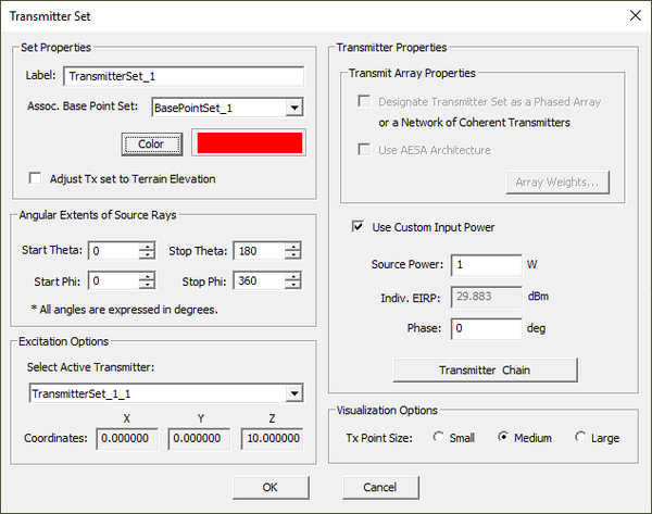
- Select Insert New Transmitter Set... to open up the Transmitter Set Dialog.
- From the drop-down list labeled Select Base Point Set, choose the desired base location set, which can be a single point object or a point array.
PYTHON COMMAND transmitter_set(label,radiator_set[,power,phase,rin_ant,xin_ant])
POINT TRANSMITTER SET PARAMETERS
| Parameter Name | Value Type | Units | Default Value | Notes |
|---|---|---|---|---|
| baseband power | real numeric | Watts | 1 | total transmitted power |
| phase | real numeric | degrees | 0 | phase of transmitted signal |
Probe Gap Circuit Load
MODULE: EM.Picasso
FUNCTION: Places a general series-parallel RLC circuit in the middle of an embedded vertical PEC via object
TO DEFINE A PROBE GAP CIRCUIT:
- Right-click on the Probe Gap Circuits item in the navigation tree.
- Select Insert New Source... to open up the Lumped Device Dialog.
- From the Host drop-down list, select a PEC Via object set.
- For "Lumped Circuit Type", select the Passive RLC radio button.
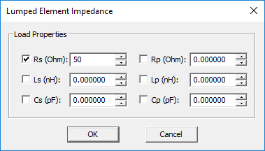
- Click the Impedance... button of the dialog to open up the Lumped Element Impedance dialog. The default series resistance is 50Ω. Check all the boxes for the series or parallel R, L, C elements as desired and enter values for the resistances, capacitances and inductances.
- Click the OK buttons of the dialogs to return to the project workspace.
PYTHON COMMAND: (Only a series resistor when amplitude is set equal to zero.)
probe_src(label,via_object,polarity[,amplitude,phase,resistance])
PROBE GAP LOAD PARAMETERS
| Parameter Name | Value Type | Units | Default Value | Notes |
|---|---|---|---|---|
| Rs | real numeric | Ohms | 50 | series resistor (must be checked) |
| Ls | real numeric | nH | - | series inductor (must be checked) |
| Cs | real numeric | pF | - | series capacitor (must be checked) |
| Rs | real numeric | Ohms | - | parallel resistor (must be checked) |
| Ls | real numeric | nH | - | parallel inductor (must be checked) |
| Cs | real numeric | pF | - | parallel capacitor (must be checked) |
Probe Gap Circuit Source
MODULE: EM.Picasso
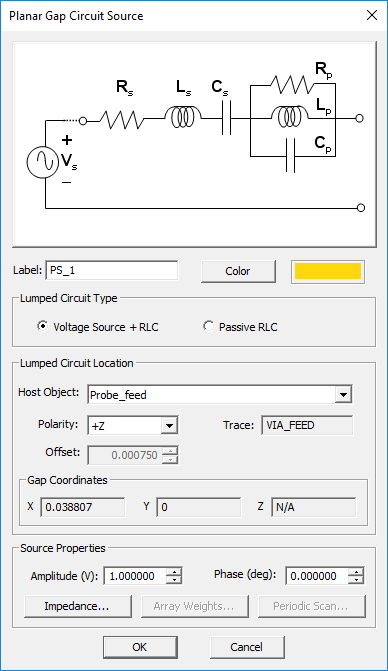
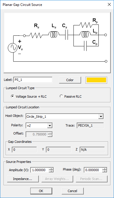
FUNCTION: Creates an infinitesimal gap across the middle of a vertical PEC via object and places an ideal voltage source with a series internal resistor
TO DEFINE A PROBE GAP SOURCE:
- Right-click on the Probe Gap Circuits item in the navigation tree.
- Select Insert New Source... to open up the Probe Gap Source Dialog.
- From the Host drop-down list, select a PEC via object.
- The probe gap source is always placed in the middle of the PEC via object.
- Click the OK button of the dialog to return to the project workspace.
PYTHON COMMAND: probe_src(label,via_object,polarity[,amplitude,phase,resistance])
PROBE GAP SOURCE PARAMETERS
| Parameter Name | Value Type | Units | Default Value | Notes |
|---|---|---|---|---|
| polarity | List: pos, neg | - | pos | polarity of the voltage source |
| amplitude | real numeric | Volts | 1 | amplitude of voltage source at the gap |
| phase | real numeric | degrees | 0 | phase of voltage source at the gap |
Resistor
MODULE: EM.Tempo
FUNCTION: Places a resistor at a specified point on a PEC line object that is parallel to one of the three principal axes
TO DEFINE A RESISTOR:
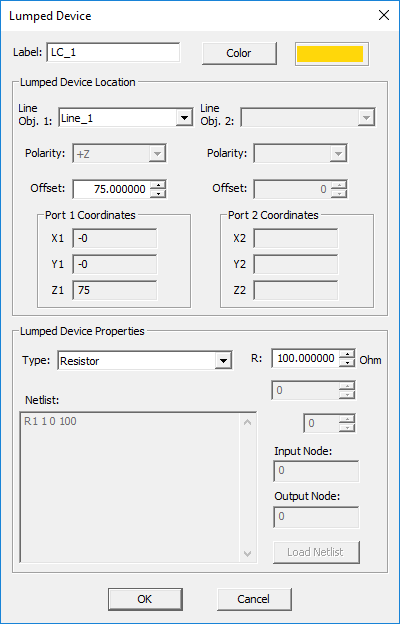
- Right-click on the Lumped Devices item in the navigation tree.
- Select Insert New Source... to open up the Lumped Device Dialog.
- From the Host drop-down list, select a line object. Note that only line parallel to one of the three principal axes are listed.
- From the Type drop-down list, select Resistor.
- By default, the lumped device is placed at the midpoint of the host line object. You can modify the Offset parameter, which is measured from the start point of the line and is always positive.
- Enter a value for Resistance in Ohms. The default resistance is 100Ω.
- Click the OK button of the dialog to return to the project workspace.
PYTHON COMMAND: resistor(label,line_object,offset,resistance)
LUMPED RESISTOR PARAMETERS
| Parameter Name | Value Type | Units | Default Value | Notes |
|---|---|---|---|---|
| offset | real numeric | project units | half the length of host line object | distance between the device and the start point of the host line object |
| resistance | real numeric | Ohms | 50 | - |
Scattering Wave Port
MODULE: EM.Picasso
FUNCTION: Creates an infinitesimal gap across a PEC rectangle strip object at a specified location and places an ideal voltage source with a series internal resistor
TO DEFINE A SCATTERING WAVE PORT:
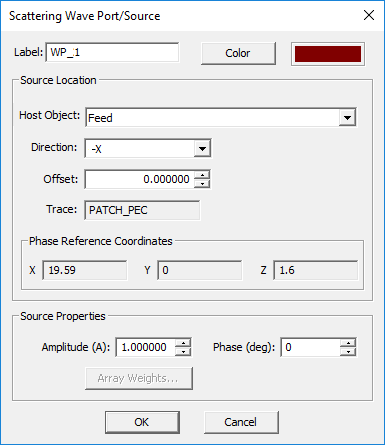
- Right-click on the Scattering Wave Ports item in the navigation tree.
- Select Insert New Source... to open up the Wave Port Dialog.
- From the Host drop-down list, select a PEC rectangle strip object.
- By default, the wave port is placed at one end of the host rect strip object. The incident wave propagates along the host strip towards this end. You can change the direction of the incident wave. You can also modify the Offset parameter, which is measured from the endpoint of the host strip. This establishes the phase reference plane for computation of the scattering parameters.
- Click the OK button of the dialog to return to the project workspace.
NOTES, SPECIAL CASES OR EXCEPTIONS: A scattering wave port is made up of a gap source that is placed close to an open end of a rectangle strip representing a feed line. The other end of the line is typically connected to a planar structure of interest. in the process of planar mesh generation, EM.Picasso automatically extends the length of a port line that hosts a scattering wave port to about two effective wavelengths. This is done to provide enough length for formation of a clean standing wave current pattern. The effective wavelength of a transmission line for length extension purposes is calculated in a similar manner as for the planar mesh resolution. It is defined as [math]\lambda_{eff} = \tfrac{\lambda_0}{\sqrt{\varepsilon_{eff}}}[/math], where εeff is the effective permittivity. For metal and conductive sheet traces, the effective permittivity is defined as the larger of the permittivities of the two substrate layers just above and below the metallic trace. For slot traces, the effective permittivity is defined as the mean (average) of the permittivities of the two substrate layers just above and below the metallic trace. The host port line must always be open from one end to allow for its length extension. You have to make sure that there are no objects standing on the way of the extended port line to avoid any unwanted overlaps.
PYTHON COMMAND: wave_port(label,rect_object,offset,is_negative[,amplitude,phase])
SCATTERING WAVE PORT PARAMETERS
| Parameter Name | Value Type | Units | Default Value | Notes |
|---|---|---|---|---|
| direction | List: pos, neg | - | pos | direction of the incident wave |
| offset | real numeric | project units | 0 | distance between the source and the endpoint of the host strip object |
| amplitude | real numeric | Volts | 1 | amplitude of incident wave |
| phase | real numeric | degrees | 0 | phase of incident wave |
RELATED LINKS: Calculating Scattering Parameters Using Prony's Method
Series RL Device
MODULE: EM.Tempo
FUNCTION: Places a collocated series combination of a resistor and an inductor at a specified point on a PEC line object that is parallel to one of the three principal axes
TO DEFINE A SERIES RL DEVICE:
- Right-click on the Lumped Devices item in the navigation tree.
- Select Insert New Source... to open up the Lumped Device Dialog.
- From the Host drop-down list, select a line object. Note that only lines parallel to one of the three principal axes are listed.
- From the Type drop-down list, select Series RL.
- By default, the lumped device is placed at the midpoint of the host line object. You can modify the Offset parameter, which is measured from the start point of the line and is always positive.
- Enter a value for Resistance in Ohms and a value for Inductance in nH. The default values are 100Ω and 1nF, respectively.
- Click the OK button of the dialog to return to the project workspace.
PYTHON COMMAND: None
LUMPED SERIES RL DEVICE PARAMETERS
| Parameter Name | Value Type | Units | Default Value | Notes |
|---|---|---|---|---|
| offset | real numeric | project units | half the length of host line object | distance between the device and the start point of the host line object |
| resistance | real numeric | Oms | 100 | |
| inductance | real numeric | nH | 1 | - |
Slot Trace
MODULE: EM.Picasso
FUNCTION: Defines a slot trace object group on an infinite PEC ground plane
TO DEFINE A SLOT TRACE GROUP:
- Right-click on the Slot Traces item in the navigation tree.
- Select Insert New Slot Trace... to open up the New Slot Trace dialog.
- The only properties of a slot trace group you can modify is its color and texture.
- Click the OK button of the dialog to return to the project workspace.
PYTHON COMMAND: slot_group(label)
SLOT TRACE PARAMETERS
| Parameter Name | Value Type | Units | Default Value | Notes |
|---|---|---|---|---|
| Locked mesh density | Real Numeric | cells/effective wavelength | 30 | Only if "Lock Mesh" enabled |
Strip Gap Circuit Load
MODULE: EM.Oicasso, EM.Libera
FUNCTION: Places a general series-parallel RLC circuit at a specified point on a PEC rectangle strip object
TO DEFINE A STRIP GAP CIRCUIT:
- Right-click on the Strip Gap Circuits item in the navigation tree.
- Select Insert New Source... to open up the Lumped Device Dialog.
- From the Host drop-down list, select a rectangle strip object.
- For "Lumped Circuit Type", select the Passive RLC radio button.
- By default, the lumped device is placed at the midpoint of the host rectangle strip object. You can modify the Offset parameter, which is measured from the center of the strip and can be either positive or negative.
- Click the Impedance... button of the dialog to open up the Lumped Element Impedance dialog. The default series resistance is 50Ω. Check all the boxes for the series or parallel R, L, C elements as desired and enter values for the resistances, capacitances and inductances.
- Click the OK buttons of the dialogs to return to the project workspace.
PYTHON COMMAND: (Only a series resistor when amplitude is set equal to zero.)
rect_gap_src(label,rect_object,offset,polarity[,amplitude,phase,resistance])
STRIP GAP LOAD PARAMETERS
| Parameter Name | Value Type | Units | Default Value | Notes |
|---|---|---|---|---|
| offset | real numeric | project units | half the length of host rectangle strip object | distance between the device and the center of the host strip object |
| Rs | real numeric | Ohms | 50 | series resistor (must be checked) |
| Ls | real numeric | nH | - | series inductor (must be checked) |
| Cs | real numeric | pF | - | series capacitor (must be checked) |
| Rs | real numeric | Ohms | - | parallel resistor (must be checked) |
| Ls | real numeric | nH | - | parallel inductor (must be checked) |
| Cs | real numeric | pF | - | parallel capacitor (must be checked) |
Strip Gap Circuit Source
MODULE: EM.Picasso, EM.Libera
FUNCTION: Creates an infinitesimal gap across a PEC rectangle strip object at a specified location and places an ideal voltage source with a series internal resistor
TO DEFINE A STRIP GAP SOURCE:
- Right-click on the Strip Gap Circuits item in the navigation tree.
- Select Insert New Source... to open up the Strip Gap Source Dialog.
- From the Host drop-down list, select a PEC rectangle strip object.
- By default, the strip gap source is placed at the midpoint of the host rect strip object. You can modify the Offset parameter, which is measured from the midpoint of the host strip and can be either positive or negative.
- Click the OK button of the dialog to return to the project workspace.
PYTHON COMMAND: rect_gap_src(label,rect_object,offset,polarity[,amplitude,phase,resistance])
STRIP GAP SOURCE PARAMETERS
| Parameter Name | Value Type | Units | Default Value | Notes |
|---|---|---|---|---|
| polarity | List: pos, neg | - | pos | polarity of the voltage source |
| offset | real numeric | project units | 0 | distance between the source and the midpoint of the host strip object |
| amplitude | real numeric | Volts | 1 | amplitude of voltage source at the gap |
| phase | real numeric | degrees | 0 | phase of voltage source at the gap |
Terrain Surface
MODULE: EM.Terrano
FUNCTION: Defines a terrain surface block group
TO DEFINE A TERRAIN SURFACE GROUP:
- Right-click on the Terrain Surfaces item in the navigation tree.
- Select Insert New Terrain... to open up the Terrain Surface dialog.
- In the material table, the default setting shows Rock with a relative permittivity of εr = 5 and an electric conductivity of σ = 0.001S/m.
- You can change the default material composition by selecting and highlighting it in the table and clicking the Add/Edit button of the dialog.
- In the Material Layer Properties dialog, either enter new values for εr and σ or click the Material button of this dialog to open EM.Cube's Materials List and select one of its entries.
- You can add several layers to your terrain surface composition. In that case, you need to define a thickness for each layer. The bottommost layer always has an infinite thickness representing an unbounded half-space medium as seen by an incident ray.
- After you complete the definition of all layers, click the OK button of the dialog to return to the project workspace.
PYTHON COMMAND: terrain_group(label,epsilon,sigma[,rr,gg,bb])
TERRAIN SURFACE PARAMETERS
| Parameter Name | Value Type | Units | Default Value | Notes |
|---|---|---|---|---|
| epsilon | Real Numeric | - | 5 | relative permittivity |
| sigma | Real Numeric | S/m | 5e-3 | electric conductivity |
| Locked mesh density | Real Numeric | cells/effective wavelength | 30 | Only if "Lock Mesh" enabled |
Thin Wire
FUNCTION: Defines a thin wire object group with a specified wire radius
TO DEFINE A THIN WIRE GROUP:
- Right-click on the Thin Wires item in the navigation tree.
- Select Insert New Thin Wire... to open up the Thin Wire dialog.
- Enter a value for the Wire Radius.
- Click the OK button of the dialog to return to the project workspace.
PYTHON COMMAND: thinwire_group(label,radius)
THIN WIRE PARAMETERS
| Parameter Name | Value Type | Units | Default Value | Notes |
|---|---|---|---|---|
| Wire radius | Real Numeric | project units | 0.3 | - |
| Locked mesh density | Real Numeric | cells/effective wavelength | 50 | "Lock Mesh" enabled by default |
Virtual Object Group
MODULE: EM.Terrano
FUNCTION: Defines a virtual object group that will be invisible to the simulation engine
TO DEFINE A VIRTUAL OBJECT GROUP:
- Right-click on the Virtual Objects item in the navigation tree.
- Select Insert a Virtual Material... to open up the Virtual Material dialog.
- Virtual materials have only one property, which is their color. You can the change from this dialog.
- Click the OK button of the dialog to return to the project workspace.
PYTHON COMMAND: virtual_group(label)
VIRTUAL OBJECT PARAMETERS: None
Volume Charge
MODULE: EM.Ferma
FUNCTION: Defines a volume charge source group with a specified charge density
TO DEFINE A VOLUME CHARGE GROUP:
- Right-click on the Volume Charges item in the navigation tree.
- Select Insert New Volume Charge... to open up the Volume Charge Source dialog.
- You have two options to choose from: Uniform and Inhomogeneous.
- If you choose the uniform option, you have to enter a numeric value for Charge Density in C/m^3.
- If you choose the inhomogeneous option, you have to enter an expression for Charge Density in the global (x,y,z) coordinates.
- Click the OK button of the dialog to return to the project workspace.
PYTHON COMMAND: charge_group(label,density)
VOLUME CHARGE PARAMETERS
| Parameter Name | Value Type | Units | Default Value | Notes |
|---|---|---|---|---|
| density | Real Numeric | C/m^3 | -1e-5 | volume charge density with a positive or negative sign |
Volume Current
MODULE: EM.Ferma
FUNCTION: Defines a volume current source group with a specified current density vector
TO DEFINE A VOLUME CURRENT GROUP:
- Right-click on the Volume Currents item in the navigation tree.
- Select Insert New Volume Current... to open up the Volume Current Source dialog.
- You have two options to choose from: Uniform and Inhomogeneous.
- If you choose the uniform option, you have to enter three numeric values for the three components of volume current density Jx, Jy and Jz in A/m^2.
- If you choose the inhomogeneous option, you have to enter three expressions for the three components of volume current density Jx, Jy and Jz in the global (x,y,z) coordinates.
- Click the OK button of the dialog to return to the project workspace.
PYTHON COMMAND: volume_current_group(label,Jx,Jy,Jz)
VOLUME CURRENT PARAMETERS
| Parameter Name | Value Type | Units | Default Value | Notes |
|---|---|---|---|---|
| Jx | Real Numeric | A/m^2 | 0.0 | X-component of volume current density vector |
| Jy | Real Numeric | A/m^2 | 0.0 | Y-component of volume current density vector |
| Jz | Real Numeric | A/m^2 | 1.0 | Z-component of volume current density vector |
Volume Heat Source
MODULE: EM.Ferma
FUNCTION: Defines a volume heat source group with a specified heat density
TO DEFINE A VOLUME HEAT SOURCE GROUP:
- Right-click on the Volume Heat Sources item in the navigation tree.
- Select Insert New Volume Heat Source... to open up the Volume Heat Source dialog.
- You have two options to choose from: Uniform and Inhomogeneous.
- If you choose the uniform option, you have to enter a numeric value for Heat Density in W/m^3.
- If you choose the inhomogeneous option, you have to enter an expression for Heat Density in the global (x,y,z) coordinates.
- Click the OK button of the dialog to return to the project workspace.
PYTHON COMMAND: charge_group(label,density)
VOLUME HEAT SOURCE PARAMETERS
| Parameter Name | Value Type | Units | Default Value | Notes |
|---|---|---|---|---|
| density | Real Numeric | W/m^3 | -1e-5 | volume heat density with a positive or negative sign |
Waveguide Port
MODULE: EM.Tempo
FUNCTION: Places a TE10 modal source at a specified location across a hollow PEC box object that is parallel to one of the three principal axes
TO DEFINE A WAVEGUIDE PORT:
- Right-click on the Waveguide Ports item in the navigation tree of EM.Tempo.
- Select Insert New Source... to open up the Waveguide Port Dialog.
- From the Host drop-down list, select a box object. Note that only hollow PEC box objects parallel to one of the three principal axes are listed.
- By default, the waveguide port is placed in the middle of the host box object parallel to its base. You can modify the Offset parameter, which is measured from the bottom base of the box.
- Click the OK button of the dialog to return to the project workspace.
PYTHON COMMAND: waveguide_src(label,box_object,offset,is_negative[,amplitude,phase])
WAVEGUIDE PORT PARAMETERS
| Parameter Name | Value Type | Units | Default Value | Notes |
|---|---|---|---|---|
| direction | List: pos, neg | - | - | direction of incident wave propagation |
| offset | real numeric | project units | half the height of host box object | distance between the source and the bottom base of the host box object |
Wire Current
MODULE: EM.Ferma
FUNCTION: Defines a wire current source group with a specified current and wire radius
TO DEFINE A WIRE CURRENT GROUP:
- Right-click on the Wire Current item in the navigation tree.
- Select Insert New Wire Current... to open up the Wire Current dialog.
- Enter a value for the total Current flowing in the wire in Amperes as well as a value for Wire Radius in the project units.
- You may assume that the wire current consists of multiple turns or multiple bundled wires. The default number of turns is 1, but you can change it.
- The current flowing in the wire is directional. You may need to check the box labeled Reverse Current if you prefer the opposite direction.
- Click the OK button of the dialog to return to the project workspace.
NOTES, SPECIAL CASES OR EXCEPTIONS: EM.Ferma allows you to define idealized wire current sources. You can use this source type to model filament currents or coils. Wire currents are defined using only line and polyline objects. You also need to define a current value I in Amperes and a wire radius r in the project units. The line or polyline object is then approximated as a volume current with a current density of J = I/(πr2) flowing along the line or polyline side's direction.
| |
If you draw curve CAD objects under a wire current group, they will be permanently converted to polyline objects before running the simulation engine. |
PYTHON COMMAND: wire_current_group(label,current,wire_radius)
WIRE CURRENT PARAMETERS
| Parameter Name | Value Type | Units | Default Value | Notes |
|---|---|---|---|---|
| current | Real Numeric | A | 1.0 | total current flowing through the wire |
| wire_radius | Real Numeric | project units | 0.5 | - |
| wire_count | Integer Numeric | - | 1 | number of collocated wires or loop turns |
Wire Gap Circuit Load
MODULE: EM.Libera
FUNCTION: Places a general series-parallel RLC circuit at a specified point on a PEC line object
TO DEFINE A WIRE GAP CIRCUIT:
- Right-click on the Wire Gap Circuits item in the navigation tree.
- Select Insert New Source... to open up the Lumped Device Dialog.
- From the Host drop-down list, select a line object.
- For "Lumped Circuit Type", select the Passive RLC radio button.
- By default, the lumped device is placed at the midpoint of the host line object. You can modify the Offset parameter, which is measured from the start point of the line and is always positive.
- Click the Impedance... button of the dialog to open up the Lumped Element Impedance dialog. The default series resistance is 50Ω. Check all the boxes for the series or parallel R, L, C elements as desired and enter values for the resistances, capacitances and inductances.
- Click the OK buttons of the dialogs to return to the project workspace.
PYTHON COMMAND: (Only a series resistor when amplitude is set equal to zero.)
wire_gap_src(label,line_object,offset,polarity[,amplitude,phase,resistance])
WIRE GAP LOAD PARAMETERS
| Parameter Name | Value Type | Units | Default Value | Notes |
|---|---|---|---|---|
| offset | real numeric | project units | half the length of host line object | distance between the device and the start point of the host line object |
| Rs | real numeric | Ohms | 50 | series resistor (must be checked) |
| Ls | real numeric | nH | - | series inductor (must be checked) |
| Cs | real numeric | pF | - | series capacitor (must be checked) |
| Rs | real numeric | Ohms | - | parallel resistor (must be checked) |
| Ls | real numeric | nH | - | parallel inductor (must be checked) |
| Cs | real numeric | pF | - | parallel capacitor (must be checked) |
Wire Gap Circuit Source
MODULE: EM.Libera
FUNCTION: Creates an infinitesimal gap across a PEC or thin wire line object at a specified location and places an ideal voltage source with a series internal resistor
TO DEFINE A WIRE GAP SOURCE:
- Right-click on the Wire Gap Circuits item in the navigation tree.
- Select Insert New Source... to open up the Wire Gap Source Dialog.
- From the Host drop-down list, select a PEC or thin wire line object.
- By default, the wire gap source is placed at the midpoint of the host line object. You can modify the Offset parameter, which is measured from the start point of the host line and is always positive.
- Click the OK button of the dialog to return to the project workspace.
PYTHON COMMAND: wire_gap_src(label,line_object,offset,polarity[,amplitude,phase,resistance])
WIRE GAP SOURCE PARAMETERS
| Parameter Name | Value Type | Units | Default Value | Notes |
|---|---|---|---|---|
| polarity | List: pos, neg | - | pos | polarity of the voltage source |
| offset | real numeric | project units | 0 | distance between the source and the start point of the host line object |
| amplitude | real numeric | Volts | 1 | amplitude of voltage source at the gap |
| phase | real numeric | degrees | 0 | phase of voltage source at the gap |
