EM.Libera Tutorial Lesson 1: Analyzing a Center-Fed Resonant Dipole Antenna
Contents
- 1 Objective:
- 2 What You Will Learn:
- 3 Getting Started
- 4 MoM3D Module Navigation
- 5 Creating a Wire Object
- 6 Source Definition
- 7 Mesh Generation
- 8 Defining Project Observables
- 9 Running the Wire MoM Simulation
- 10 Viewing the Simulation Results
- 11 Running a Uniform Frequency Sweep
- 12 Running an Adaptive Frequency Sweep
Objective:
To construct a center‐fed resonant dipole antenna in EM.Cube’s MoM3D Module, analyze it using the Wire MoM solver and visualize its near and far field characteristics.
What You Will Learn:
A simple half‐wave dipole antenna in free space will be analyzed in the first tutorial. This tutorial will guide you through all necessary steps required to set up and perform a basic Wire MoM simulation and visualize and graph the simulation results.
| |
We strongly recommend that you read through the first few tutorials and study them carefully before setting up your own projects. |
Getting Started
Open the EM.Cube application. Click Start, select All Programs, and then the EMAG program group. Select EM.CUBE to start the program. By default, EM.Cube opens up a blank project with the name “UntitledProj1” in its CubeCAD Module.
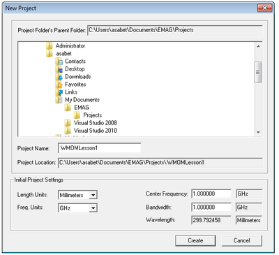
You can start drawing objects and build up your physical structure right away. Or you can initiate a new project by selecting the New ![]() button of the System Toolbar (or using the keyboard shortcut Ctrl+N, or via the menu File → New Project…). This opens up the New Project Dialog, where you can enter a title for your new project and set its path. You can use the Windows Explorer to go to the desired folder where you want to place your new project folder. For this project, use the title “WMOMLesson1”. From the same dialog, you can also set the project’s Length Units, Frequency Units, Center Frequency and Bandwidth. For this tutorial lesson, set the length and frequency units of the project to Millimeters and Gigahertz, respectively, and set both the center frequency and bandwidth to 1GHz. Then, click the Create button of the dialog to accept the settings. A new project folder with your given name is immediately created at your specified path.
button of the System Toolbar (or using the keyboard shortcut Ctrl+N, or via the menu File → New Project…). This opens up the New Project Dialog, where you can enter a title for your new project and set its path. You can use the Windows Explorer to go to the desired folder where you want to place your new project folder. For this project, use the title “WMOMLesson1”. From the same dialog, you can also set the project’s Length Units, Frequency Units, Center Frequency and Bandwidth. For this tutorial lesson, set the length and frequency units of the project to Millimeters and Gigahertz, respectively, and set both the center frequency and bandwidth to 1GHz. Then, click the Create button of the dialog to accept the settings. A new project folder with your given name is immediately created at your specified path.
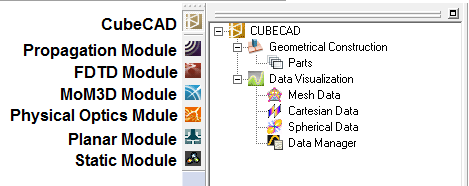
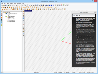 EM.Cube's project workspace. |
EM.Cube’s CubeCAD Module lets you construct 3D geometries, or import them via external model files such as *.stp, *igs, or *.stl. Once these geometries have been modified or completed, they can be moved to other modules within EM.Cube for further simulation. On the other hand, all modules of EM.Cube offer full CAD operations by themselves. Therefore, you can build a new project from the ground up in any of EM.Cube’s computational modules.
To navigate to MoM3D Module, simply select its icon from the Module Toolbar on the left side of the screen. Any module may be selected this way. Selecting the module icon changes the Navigation Tree to represent the types of objects supported by the current module. The Navigation Tree of all computational modules features the following nodes: Physical Structure, Computational Domain, Discretization, Sources, and Observables.
The default view in EM.Cube is a 3D Perspective view of the project workspace. A different view can be selected by one of the 7 window selection buttons on the View Toolbar. Further, the 3D window can be split into the Top, Front, Right, and Perspective viewports by clicking on the “Split Viewport” button. This will display four smaller windows simultaneously, allowing you to view your structure from each of these four angles at once. Clicking the “Merge Viewport” button, right next to the “Split Viewport” button, brings the split view back into a single view.
 EM.Cube's View Toolbar. |
Creating a Wire Object
Select the Line Tool from the Object Toolbar (or use the keyboard shortcut F3, or the menu Object → Curve → Line).

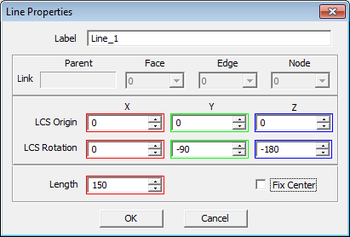
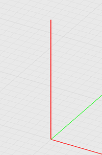
With the line tool selected, click the origin (0,0,0), and drag the mouse to start drawing a line. While still in “Draw Mode”, press and hold the Alt button of the keyboard. This forces the drawn line to be constrained along the alternate Z-axis (normal to the default XY plane on which the mouse pointer moves). Observe the changing Length value in the dialog box as you drag the mouse back and forth. When the length reaches a value of 150 units, left-click to “lock-in” the value. You may also left-click at any point and adjust the length by typing in a value of 150 in the object’s property dialog.
Since the center frequency of the project is 1GHz, the operating wavelength is:
[math] \lambda_0 = \frac{c}{f} = \frac{3e+8}{1e+9} = 0.3m = 300mm [/math]
For your resonant dipole to be half-wave, it can be approximated at 150mm.
Once your drawing is complete, you can zoom to fit your structure into the screen using the keyboard shortcut Ctrl+E or by clicking the Zoom Extents ![]() button of View Toolbar. After you have rotated or panned the view, you can always restore EM.Cube’s standard perspective view using the keyboard’s Home Key or by clicking the Perspective View
button of View Toolbar. After you have rotated or panned the view, you can always restore EM.Cube’s standard perspective view using the keyboard’s Home Key or by clicking the Perspective View ![]() button of View Toolbar.
button of View Toolbar.
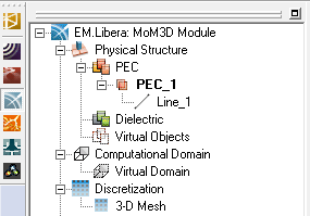
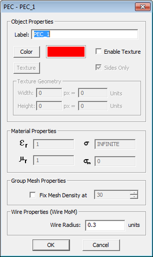
In EM.Cube’s MoM3D Module, objects are grouped together and organized by material under the “Physical Structure” node of the Navigation Tree. Since you selected no material for your line object, the first drawn object is automatically assigned a PEC_1 material group. The default perfect electric conductor (PEC) group is set as the active material. When a material group is set as active, its name appears in bold letters, and all subsequently drawn objects will be placed under that material node. Any material group can be set as the active material by right-clicking on its name in the Navigation Tree and selecting Activate from the contextual menu. All the wire objects or wireframe object belonging to the same PEC group have the same color and the same wire radius. To see this, right-click on the name of PEC_1 and select Properties... from the contextual menu. The PEC dialog opens up, where you can see the default name, default red color and the default radius wire of 0.003 units. At the center frequency of 1GHz, the default radius wire is 0.001λ0. From this dialog, you can change the name, color and wire radius of the PEC group.
Source Definition
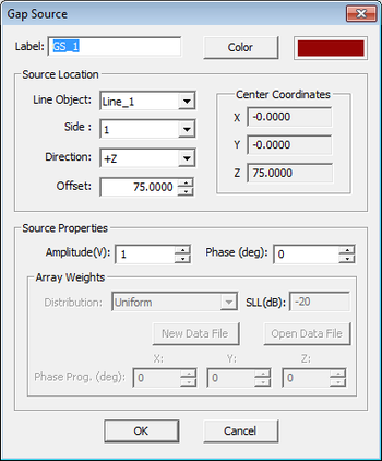
A dipole antenna can be excited using a gap source, which is the simplest source type in the MoM3D Module. A gap source can be placed on a line object (line gap), or on a rectangle strip object (strip gap) or on a box object (box gap). The line gap is intended for Wire MoM simulation, while strip and box gaps are intended for Surface MoM simulation. A line gap source creates an infinitesimal gap on the line and connects a voltage source across the gap. To define a gap source, right-click on the Gap Source item in the “Sources” section of the Navigation Tree, and select Insert New Line Gap Source… The Line Gap Source Dialog opens up.
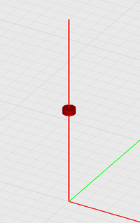
The drop-down list labeled Line Object displays all the line objects in the project workspace. In this project, there is only one object, which is selected by default. A new gap source is placed at the center of the host line object by default. The location of the source can be changed via the Offset parameter of the dialog. We will leave this at 75 for this tutorial, as we want to test a center-fed dipole. You can also change the direction of the gap source. Your gap source will have an Amplitude of 1V and a zero Phase. You will see the gap source in the middle of the line, represented by two parallel disks.
Mesh Generation
EM.Cube has several types of mesh generators that are used to discretize the physical structure for the numerical solution of Maxwell's equations. EM.Cube's MoM3D Module has two mesh generators: one for the Wire MoM solver and the other for the Surface MoM solver. The Wire MoM mesh generator discretizes line objects into a number of linear cells. It converts curve objects first into polylines and then subdivides each side of the resulting polylines. The Wire MoM mesh generator creates a wireframe version of surface and solid objects. The wireframe structure indeed consists of a set of interconnected wire segments. The current continuity is enforced at the joint shared among several interconnected wire segments. The Surface MoM mesh generator, on the other hand, creates a triangular surface mesh of surface and solid objects. It ignores any line or curve objects.
You can control the mesh resolution in two ways. The first method is to set the "Mesh Density" in the form of the number of cells per wavelength. In this case, your mesh will be frequency dependent. For example, if you set the mesh density to 10 cells per wavelength, the number of cells on a line object of fixed length will increase as the frequency increases. At an operational frequency of 1GHz, the wavelength is 300mm. Therefore, with this mesh density, you will have a total of 5 cells across your 150mm long dipole antenna. Now consider an operational frequency of 2GHz with a corresponding free-space wavelength of 150mm. With the same mesh density, your dipole antenna will have 10 cells at 2GHz. The second method of controlling the mesh is by setting a fixed "Edge Length" for the mesh cells. The edge length is set in the project units. A mesh of this kind will be frequency-independent. By default, the "Mesh Resolution" is set in terms of "Density" with a default value of 10 cells per wavelength.
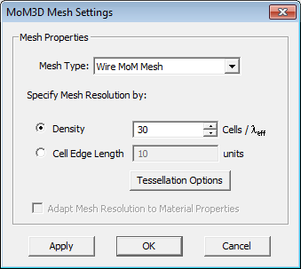
The mesh properties can be accessed by clicking the Mesh Settings ![]() button of the Simulate Toolbar (or using the keyboard shortcut Ctrl+G or via the menu Simulate → Discretization → Mesh Settings). For this tutorial, set the mesh type to "Wire MoM Mesh", keep the default "Density" option and set its value to 30 cells per wavelength. In this case, at 1GHz your dipole antenna will have 15 cells across it.
button of the Simulate Toolbar (or using the keyboard shortcut Ctrl+G or via the menu Simulate → Discretization → Mesh Settings). For this tutorial, set the mesh type to "Wire MoM Mesh", keep the default "Density" option and set its value to 30 cells per wavelength. In this case, at 1GHz your dipole antenna will have 15 cells across it.
| |
A high mesh density is recommended for resonant structures and for better visualization of current distributions. |
To view the mesh, click the Show/Generate Mesh ![]() button of the Simulate Toolbar (or alternatively use the keyboard shortcut Ctrl+M). For this particular project, the mesh view does not reveal much because the mesh of a vertical line object conforms to wire itself. In general, the mesh view shows how the simulation engine sees your physical structure.
button of the Simulate Toolbar (or alternatively use the keyboard shortcut Ctrl+M). For this particular project, the mesh view does not reveal much because the mesh of a vertical line object conforms to wire itself. In general, the mesh view shows how the simulation engine sees your physical structure.
Defining Project Observables
Project observables are output quantities that you would like to compute at the end of an FDTD simulation. By default, the Wire MoM solver does not generate any output data unless you define one or more project observables before you start a simulation.
Current Distribution
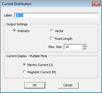
Current distribution observables are used to visualize the linear currents on the wires or wireframe structures. To define a current distribution observable, right click on the Current Distributions item in the “Observables” section of the Navigation Tree and select Insert New Observable… This opens up the Current Distribution Dialog. Keep all the default options and close the dialog. A new entry CD_1 is added to the Navigation Tree.
Radiation Patterns
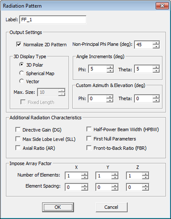
To plot the radiation patterns of a radiating structure, you need to define a far field observable. To define a far field observable, right click on the Far Fields item in the Observables section of the Navigation Tree, and select Insert New Radiation Pattern… In general, you can accept the default values, unless a special case is being analyzed.
Port Definition
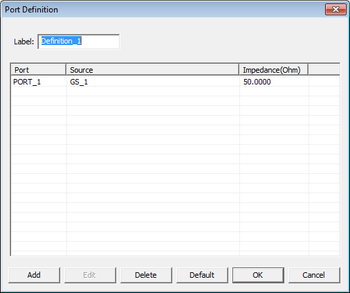
For calculating the port characteristics of the dipole antenna such as S parameters and input impedance, you need to set up a port. To do so, right click on Port Definitions under the Observables section of the Navigation Tree, and select Insert New Port Definition… By default, since you have only one source, it is assigned as Port 1. Accept the default values for PORT_1 and click OK to accept these values.
Running the Wire MoM Simulation
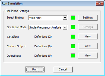
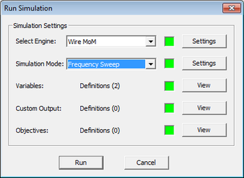
At this time, your project is ready for the Wire MoM simulation of your dipole antenna structure. Click the Run ![]() Button of the Simulate Toolbar to open up the Simulation Run Dialog. Or alternatively, use the keyboard shortcut Ctrl+R, or the menu Simulate → Run… The simplest simulation mode in EM.Cube is “Analysis”. In this mode, your physical structure is taken “As Is” and its mesh is passed to the Wire MoM simulation engine, along with the necessary information regarding the sources and observables. Since MoM simulations are frequency-domain, first you will run a "Single-Frequency Analysis". Select this option from the drop-down list labeled "Simulation Mode". Make sure you have selected the "Wire MoM" option for "Engine Type".
Button of the Simulate Toolbar to open up the Simulation Run Dialog. Or alternatively, use the keyboard shortcut Ctrl+R, or the menu Simulate → Run… The simplest simulation mode in EM.Cube is “Analysis”. In this mode, your physical structure is taken “As Is” and its mesh is passed to the Wire MoM simulation engine, along with the necessary information regarding the sources and observables. Since MoM simulations are frequency-domain, first you will run a "Single-Frequency Analysis". Select this option from the drop-down list labeled "Simulation Mode". Make sure you have selected the "Wire MoM" option for "Engine Type".
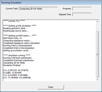
To run the simulation, click the Run button of the Simulation Run Dialog. A separate window pops up displaying messages from the simulation engine. Once the simulation is completed, you will see the values of S11, Z11 and Y11 reported in the Message Windows. In this case, you will get S11 = 0.291310 + 0.231841j, Z11 = 77.464068 + 41.698638j Ohms, and Y11 = 0.010009 - 0.005388j S. You can close the message window and return to the project workspace. The Navigation Tree is now populated with simulation results, most notably under Current Distributions and Far Fields nodes.
Viewing the Simulation Results
EM.Cube’s computational modules usually generate two types of data: 2D and 3D. Examples of 2D data are probe fields, S/Z/Y parameters and polar radiation patterns. 2D data are graphed in EM.Grid. Examples of 3D data are near field distributions and 3D radiation patterns. 3D data are visualized in EM.Cube’s project workspace and the plots are usually overlaid on the physical structure.
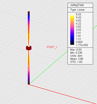
First, you will visualize the current distribution on the dipole. The "Current Distribution" section of the Navigation Tree plots both electric currents (J) and magnetic currents (M). The Wire MoM solver computes electric currents only as it can only handle PEC objects. The Surface MoM solver can handle both PEC and dielectric objects. In the case of dielectric objects, both surface electric currents and surface magnetic currents are computed. Each current distribution observable contains a list of twelve amplitude and phase plots for all the six current components: Jx, Jy, Jz, and Mx, My, Mz. There are also two additional plots for the magnitude of total electric current and total magnetic current. Click on any of these plots to display them in the project workspace. You can use the standard view operations such as dynamic zoom, rotate view, pan view, etc. to better examine these plots.
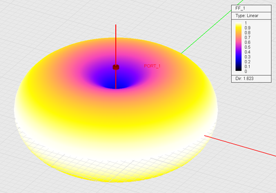
The Far Fields section of the Navigation Tree contains three different 3D radiation pattern plots: the Theta component of the far‐zone electric field, the Phi component of the far‐zone electric field, and the Total far field. You will notice that the Far Field plots are all centered at the origin of coordinates. This is due to the fact that the radiation patterns are calculated in a standard spherical coordinate system center at (0, 0 , 0). Once you are in a near field or far field visualization view, you can always go back to the Normal view mode of the project workspace using the keyboard’s Esc Key.
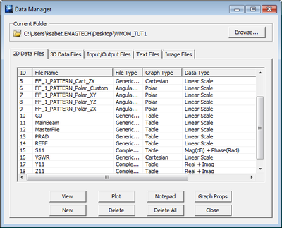
Besides 3D visualization of the radiation patterns, you can plot 2D graphs of the patterns at certain plane cuts. A list of all the 2D output data files generated at the end of a simulation can be viewed in EM.Cube’s Data Manager. To open this dialog, click the Data Manager ![]() button of Simulate Toolbar, or use the keyboard shortcut Ctrl+D, or access the menu Simulate → Data Manager, or right click on the Data Manager item in the “Observables” section of the Navigation Tree and select Open Data Manager…
button of Simulate Toolbar, or use the keyboard shortcut Ctrl+D, or access the menu Simulate → Data Manager, or right click on the Data Manager item in the “Observables” section of the Navigation Tree and select Open Data Manager…
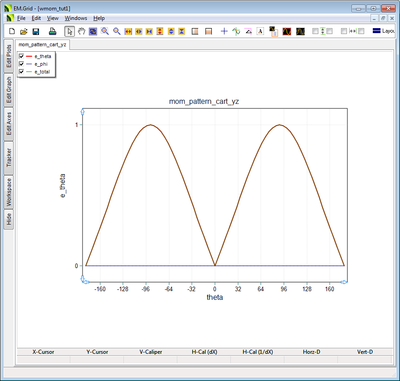
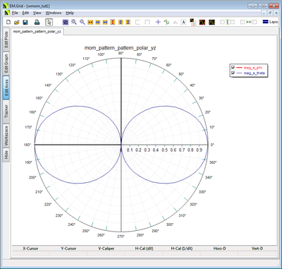
The 2D radiation patterns can be plotted as both Cartesian and polar graphs. Open up the Data Manager dialog and spot Cartesian pattern data files with a “.DAT” file extension as well as the polar (angular) data files with a “.ANG” file extension. The figure below shows the Cartesian and polar radiation pattern plots in the YZ plane cut. Besides the three principal XY, YZ and ZX plane cuts, there are also data files for one additional user defined Phi‐plane cut, which by default is calculated at φ = 45o.
Running a Uniform Frequency Sweep
To examine the frequency response of the dipole antenna, that is its port characteristics as a functions of frequency, you need to perform a frequency sweep of our structure.
Click the Run ![]() Button of the Simulate Toolbar to open up the Simultion Run Dialog. Select the "Frequency Sweep" option from the drop-down list labeled "Simulation Mode". Make sure you have selected the "Wire MoM" option for "Engine Type". Then, click on the Settings button next to the Simulation Mode drop-down list. This opens up the Frequency Settings dialog.
Button of the Simulate Toolbar to open up the Simultion Run Dialog. Select the "Frequency Sweep" option from the drop-down list labeled "Simulation Mode". Make sure you have selected the "Wire MoM" option for "Engine Type". Then, click on the Settings button next to the Simulation Mode drop-down list. This opens up the Frequency Settings dialog.
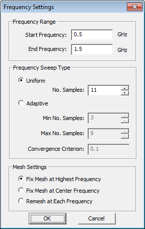
At the top you can set the Start and End frequencies for your sweep. Since your project's center frequency is 1GHz and the bandwidth is 1GHz, too, the default values of the start and end frequencies are set to 0.5GHz and 1.5GHz. For "Frequency Sweep Type", select the "Uniform" option. Set the "Number of Samples" to 11. This will sweep the frequency by setting the operational frequency of the project to 0.5GHz, 0.6GHz, ..., 1.4GHz, 1.5GHz.
To start the sweep simulation, click the Run button of the Simulation Run Dialog. The message window pops up and reports the calculated port characteristics as the simulation proceeds. Close the window at the end of the sweep simulation and return to the project workspace.
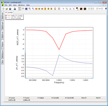
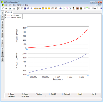
To examine the port characteristics of the dipole antenna, open up the Data Manager again. The S/Z/Y parameters are written into complex data files with a “.CPX” file extension. To graph the S11 and Z11 parameters, select the files “S11_Sweep.CPX” and “Z11_Sweep.CPX”. You can view the contents of the two files using the View button of Data Manager. To plot them in EM.Grid, click the Plot button of the dialog. By default, the S parameters are plotted on magnitude/phase Cartesian graphs, while the Z and Y parameters are plotted on real/imaginary Cartesian graphs.
Running an Adaptive Frequency Sweep
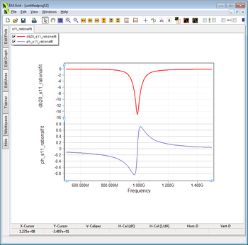
In the previous part, you saw a plot of the S11 parameter and noted that it has a resonant dip at 1GHz. However, since you swept the frequency every 100MHz, the plot was rather choppy. In a uniform frequency sweep, the calculated values are simply connected to each other (linearly interpolated) to produce the S11 graph. If you prefer a smooth graph, EM.Cube offers a second frequency sweep type called "Adaptive Sweep".
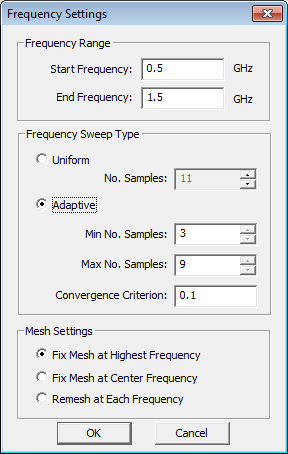
Click the Run ![]() Button of the Simulate Toolbar to open up the Simultion Run Dialog. Select the "Frequency Sweep" option from the drop-down list labeled "Simulation Mode" and open up the Frequency Settings dialog. Set the Frequency Sweep Type to Adaptive and accept its default values. Start the sweep simulation by clicking the Run button of the Simulation Run Dialog. During an adaptive simulation, the frequency samples are chosen by EM.Cube in an adaptive manner to capture the special features of the frequency response. Rational approximation of the computed samples are utilized to generate smooth curves of the port characteristics. During the adaptive sweep simulation, the program may pop up a warning that the convergence criterion has not be achieved during the first round, and ask if you would like to continue the sweep. Instruct to continue until convergence is achieved and the sweep completes successfully.
Button of the Simulate Toolbar to open up the Simultion Run Dialog. Select the "Frequency Sweep" option from the drop-down list labeled "Simulation Mode" and open up the Frequency Settings dialog. Set the Frequency Sweep Type to Adaptive and accept its default values. Start the sweep simulation by clicking the Run button of the Simulation Run Dialog. During an adaptive simulation, the frequency samples are chosen by EM.Cube in an adaptive manner to capture the special features of the frequency response. Rational approximation of the computed samples are utilized to generate smooth curves of the port characteristics. During the adaptive sweep simulation, the program may pop up a warning that the convergence criterion has not be achieved during the first round, and ask if you would like to continue the sweep. Instruct to continue until convergence is achieved and the sweep completes successfully.
Open up the Data Manager again. At the end of an adaptive sweep, the originally computed S/Z/Y parameters are written into the complex data files “S11.CPX”, “Z11.CPX” and “Y11.CPX”, while the rationally interpolated port characteristics (the resulting smooth curves) are written into the complex data files “S11_RationalFit.CPX”, “Z11_RationalFit.CPX” and “Y11_RationalFit.CPX”. Select “S11_RationalFit.CPX” and plot it in EM.Grid. As shown in the figure below, the rational approximation of S11 thus calculated is quite smooth and can adequately capture its resonance behavior around 1GHz.

