EM.Tempo Tutorial Lesson 7: Modeling a Periodic Frequency Selective Surface
Contents
Objective:
To construct a frequency selective surface made of periodic printed strips on a thick dielectric substrate and examine its reflection and transmission characteristics.
What You Will Learn:
In this tutorial you will learn how to define periodic structures in EM.Cube's FDTD Module and excite them using plane wave sources. You will get familiar with the subtleties of the constant transverse wavenumber method when handling oblique incident angles.
Getting Started
Open the EM.Cube application and switch to FDTD Module. Start a new project with the following attributes:
- Name: FDTDLesson6
- Length Units: mm
- Frequency Units: GHz
- Center Frequency: 9GHz
- Bandwidth: 18GHz
Building the Periodic Unit Cell Structure
Define a new dielectric material with εr = 2.2, μr = 1, σ = 0 and σm = 0. With the Dielectric_1 group active, draw a box of dimensions 15mm × 15mm × 6mm to represent the thick substrate. Set the local coordinate system (LCS) of the box object at (0, 0, 0). Next, define a PEC group like PEC_1 and activate it. Draw a rectangle strip of length 12mm and width 3mm (3,12) to represent the printed strip. Place the strip at the center of the top face of the dielectric objects at (0, 0, 6mm).
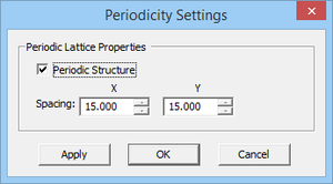
Next, right-click on the Periodicity item in the Computational Domain section of the Navigation Tree and select Periodicity Settings from the contextual menu. In the Periodicity Settings dialog, check the box labeled Periodic Structure. The domain box shrinks to the edges of the dielectric box and the X Spacing and Y Spacing are both set equal to 15mm automatically. Accept these default values.
Define a downward-looking, normally incident plane wave source with TEz Polarization. Keep the default incident angles of θ = 180° and φ = 0°. Note that unlike regular, aperiodic structures, in which the plane wave box encloses the entire physical structure, here you see a purple plane placed at a certain height above the periodic structure. For periodic structures in FDTD, the plane wave source is enforced at a plane placed at a certain Z-coordinate. The default periodic source plane is placed 0.15λ0 above (or blow) the largest bounding box of the physical structure. You can change its location from the Plane Wave Dialog. In the section titled Excitation Box in WCS, select the radio button labeled Custom. This enables the coordinate boxes for Corner 1 Node and Corner 2 Node. Unlike regular, aperiodic structures, in which all the six coordinate boxes are enabled, in the periodic case only the Z-coordinate of Corner 1 Node becomes available for editing. The Z-coordinate of Corner 2 Node is always equal to the Z-coordinate of Corner 1 Node, because you have a source plane in this case (not a source box). For this tutorial lesson, you will keep the Default options of the Excitation Box and leave its settings unchanged.
As for the project observables, define a Z-directed field sensor and position its plane at Z = 6mm (i.e. plane of the strip). Also, define an X-directed field probe and position it at (1.5mm, 0, 6mm), which is the center of right edge of the metallic strip.
Running a Periodic FDTD Analysis
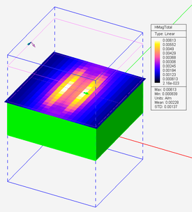
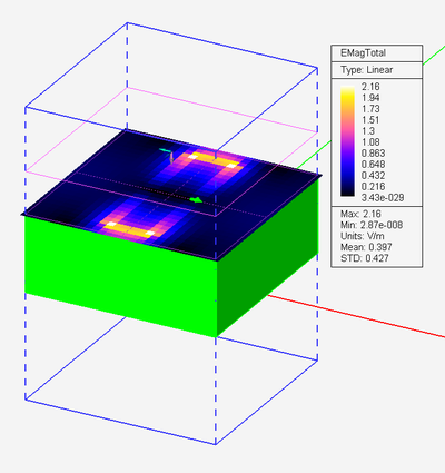
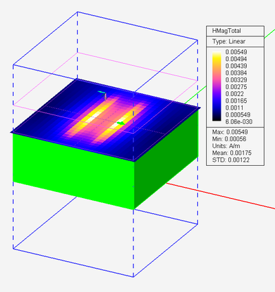
Run a quick FDTD Analysis and visualize the near field distributions. In particular, plot the Cartesian graph of the magnitude of the X component (Hx) of the magnetic field in EM.Grid. This corresponds to the electric surface current on the strip. As you would expect, there is a strong current and a high H-field value at the location of Probe_1, which happens to be at the center of the right edge of the strip.
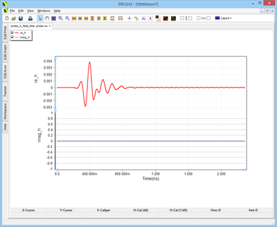
Next, graph the field data collected by your time domain probe in EM.Grid. Open the Data Manager and select the file “Probe_1_H_Time.CPX” from the data file list. Note that for periodic structures, the time domain field probes generate complex field data. This is due to the fact that EM.Cube uses the direct spectral FDTD method (also known as the constant transverse wavenumber method) to solve periodic structures. In this formulation, all the six electric and magnetic field components have complex temporal variations at all points in the space. That is why the time domain probe field data file has a “.CPX” file extension. The Cartesian graph plots the real andimaginary parts of the Hx component as a function of time. As you can see from the figure, the field dies off quickly.
Finally, plot the graphs of the reflection and transmission coefficients of your periodic structure. This can be done conveniently by right clicking on the Periodic Characteristics item in the Observables section of the Navigation Tree and selecting either Plot Reflection Coefficient… or Plot Transmission Coefficient… from the contextual menu. You can also plot these graphs from the Data Manager through the output data files “reflection_coefficient.CPX” and “transmission_coefficient.CPX”. The plots show the variation of the reflection and transmission (R/T) coefficients with frequency over the specified bandwidth of your project.
Examining a Case of Oblique Incidence
Next, you will illuminate the periodic structure with an obliquely incident plane wave source. Open the property dialog of the plane wave source and change its Theta incident angle to 135°. This is an obliquely incident plane wave that illuminates your periodic unit cell from the left side at an angle of 45° with respect to the zenith. Keep in mind that the spherical incident angles (θ, φ) of a plane wave source in EM.Cube correspond to its propagation vector.
Run a new FDTD analysis and wait until it is completed. Visualize the simulation results. The Hx field distribution on the field sensor plane looks similar to the previous case of normal incidence, except for the fact that the right edge of the metallic strip is a little bit “hotter” than its left edge. Then, graph the time domain probe’s field data in EM.Grid. You will see a completely different picture this time. A large number of slowly damping oscillations are observed along the time axis.
If you view the contents of the data files in Data Manager, you will find that both files contain only one frequency data point, which is the center frequency of the project.
R: -8.963041e-001 2.046012e-001
T: 2.932739e-001 -2.424009e-001
| |
In the case of an oblique plane wave incidence, EM.Cube's FDTD Module computes the reflection and transmission coefficients of a period structure only at the center frequency of the project. |
At a center frequency of 9GHz and a incident plane wave angle of θ = 135°, the transverse wavenumber is calculated to be:
[math] k_l = k_0 sin\theta = \frac{2\pi f}{c} sin\theta = \frac{(2\pi)(9e+9)}{3e+8} sin(135\deg) = 133.286 m^{-1} [/math]
The value of the transverse wavenumber kl is kept constant during the FDTD simulation. This limits the frequency bandwidth of FDTD’s temporal waveform (i.e., the modulate Gaussian pulse) due to the appearance of a horizontal resonant frequency at:
[math] f_{res} = f_0 sin\theta = (9GHz)sin(135\deg) = 6.364GHz [/math]
This resonant frequency indeed corresponds to an incident angle of θ = 90° (a laterally propagating wave) for the same constant value of kl = 133.286 m-1. EM.Cube automatically adjusts the temporal waveform of the FDTD simulation engine by pushing the modulation frequency away from fres to avoid horizontal resonances. In fact, the FDTD simulation results are correct at the center frequency of project with the specified incident θ angle, as well as at all the (fi, θi) pairs such as
[math] \frac{2\pi f_i}{c} sin\theta_i = k_l = const. [/math]
Running a Frequency Sweep
Although for the case of an obliquely incident plane wave source, the reflection and transmission coefficients were calculated at the center frequency of the project, you can run a parametric sweep with the center frequency being your sweep variable. This is indeed identical to EM.Cube's other modules' frequency sweep. The FDTD Module does not offer a separate frequency sweep option because in most cases it provides wideband frequency data. To define a parametric sweep, open the Run Dialog and select Parametric Sweep from the Simulation Mode drop-down list. Click the Settings button next to this drop-down list to open up the Sweep Settings Dialog. On the table on the left you see two variables: fc representing the center frequency and bw representing bandwidth. Select fc and move it to the table on the right using the right arrow (-->) button. This opens up another dialog for you enter the start, stop and step values of the sweep variable. Enter 3e+9 (3GHz) for the start frequency, 15e+9 (15GHz) for the stop frequency, and 1e+9 (1GHz) for the frequency step. Close both dialogs to return to the Run dialog. At this time, you can start the sweep simulation. Wait until all the frequency samples are computed. Then, plot the Cartesian graphs of the R/T coefficients in EM.Grid.
