Difference between revisions of "EM.Tempo"
(→Radiation Pattern Above A Half-Space Medium) |
(→Waveforms & Discrete Fourier Transforms) |
||
| Line 887: | Line 887: | ||
Since a Gaussian pulse waveform has considerable DC content, it must be used to model lowpass structures. In that case, the center frequency and bandwidth of the project must be set such that Δf = 2f<sub>0</sub> and hence, f<sub>min</sub> = f<sub>0</sub> - Δf/2 = 0, and f<sub>max</sub> = f<sub>0</sub> + Δf/2 = 2f<sub>0</sub>. The width t of the temporal Gaussian pulse is then determined such that at f<sub>max</sub> the spectral Gaussian pulse drops to the d-level from its maximum value of 1. With a bandwidth of Δf, the pulse width must satisfy the following equation: | Since a Gaussian pulse waveform has considerable DC content, it must be used to model lowpass structures. In that case, the center frequency and bandwidth of the project must be set such that Δf = 2f<sub>0</sub> and hence, f<sub>min</sub> = f<sub>0</sub> - Δf/2 = 0, and f<sub>max</sub> = f<sub>0</sub> + Δf/2 = 2f<sub>0</sub>. The width t of the temporal Gaussian pulse is then determined such that at f<sub>max</sub> the spectral Gaussian pulse drops to the d-level from its maximum value of 1. With a bandwidth of Δf, the pulse width must satisfy the following equation: | ||
| − | [[Image:FDTD64(1).png]] | + | :<math> |
| + | \exp[-(\pi f_{\delta} \tau)^2] = \exp[-(\pi \Delta f \tau)^2] = \delta | ||
| + | \quad \Rightarrow \quad | ||
| + | \tau = \frac{\sqrt{-\ln\delta}}{\pi f_{max}} | ||
| + | </math> | ||
| + | <!--[[Image:FDTD64(1).png]]--> | ||
When you set δ = 0.1 (the default value), it means that the Fourier transform of your excitation waveform drops to 10% of its peak at the upper edge of your specified frequency range. For a Modulated Gaussian pulse waveform with a bandwidth of Δf, the pulse width must satisfy the following equation: | When you set δ = 0.1 (the default value), it means that the Fourier transform of your excitation waveform drops to 10% of its peak at the upper edge of your specified frequency range. For a Modulated Gaussian pulse waveform with a bandwidth of Δf, the pulse width must satisfy the following equation: | ||
| − | [[Image:FDTD65.png]] | + | :<math> |
| + | \exp[ -[\pi(f_{\delta} - f_0)\tau] ^2 ] = \exp \left[ -\left(\pi \frac{\Delta f}{2} \tau\right)^2 \right] = \delta | ||
| + | \quad \Rightarrow \quad | ||
| + | \tau = \frac{2\sqrt{-\ln \delta}}{\pi \Delta f} | ||
| + | </math> | ||
| + | <!--[[Image:FDTD65.png]]--> | ||
For the default value of δ = 0.1, you get the standard relation: τ = 0.966 / BW, which is typically used for modulated Gaussian waveforms. The source waveform requires a time delay t<sub>0</sub> so that its value drops to almost zero at t = 0. The time delay is expressed in terms of a multiple of the pulse width: '''t0 / tau''', and its default value is 4.5. | For the default value of δ = 0.1, you get the standard relation: τ = 0.966 / BW, which is typically used for modulated Gaussian waveforms. The source waveform requires a time delay t<sub>0</sub> so that its value drops to almost zero at t = 0. The time delay is expressed in terms of a multiple of the pulse width: '''t0 / tau''', and its default value is 4.5. | ||
| Line 897: | Line 907: | ||
Keep in mind that FDTD is a time domain algorithm. At the end of an FDTD simulation, a Discrete Fourier Transform (DFT) is performed on the time domain data to calculate frequency domain characteristics such as near fields, far field radiation patterns, RCS, S/Y/Z parameters, etc.: | Keep in mind that FDTD is a time domain algorithm. At the end of an FDTD simulation, a Discrete Fourier Transform (DFT) is performed on the time domain data to calculate frequency domain characteristics such as near fields, far field radiation patterns, RCS, S/Y/Z parameters, etc.: | ||
| − | [[Image:FDTD68.png]] | + | :<math> |
| + | \tilde{F}(f) = \int_{-\infty}^{\infty} f(t) e^{-j2\pi f t} \, dt | ||
| + | \quad \approx \quad | ||
| + | \Delta t \sum_{n=0}^N f(n\Delta t) e^{-j2 \pi n f \Delta t} | ||
| + | </math> | ||
| + | <!--[[Image:FDTD68.png]]--> | ||
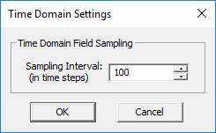
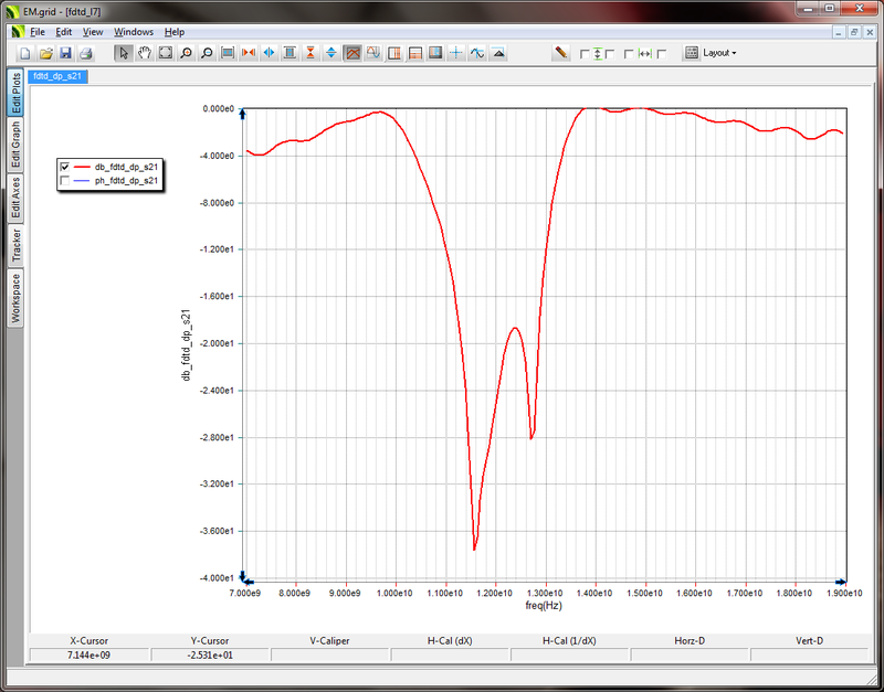
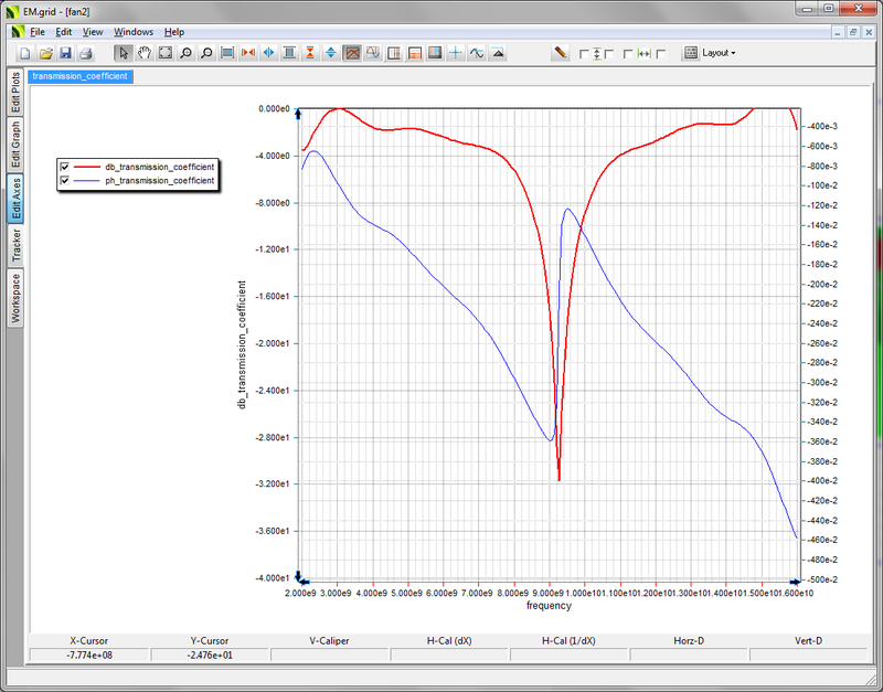
Of [[FDTD Module]]'s observables, the near fields, far fields and all of their associated parameters like directivity, RCS, etc., are calculated at a certain frequency that is specified as part of the definition of the observable. On the other hand, port characteristics like S/Y/Z parameters, VSWR and periodic characteristics like reflection and transmission coefficients, are calculated over the entire specified bandwidth of your project. In other words, you get a wideband frequency response at the end of a single time domain FDTD simulation run. The number of frequency point data over this bandwidth is equal to the number of DFT samples that are generated during the time marching loop. This number is set to 200 by default. In other words, 200 frequency data are generated at the end of an FDTD simulation. You can change this number through the box labeled '''No. DFT Samples''' in the "Discrete Fourier Transform" section of the FDTD Simulation Engine Settings dialog. | Of [[FDTD Module]]'s observables, the near fields, far fields and all of their associated parameters like directivity, RCS, etc., are calculated at a certain frequency that is specified as part of the definition of the observable. On the other hand, port characteristics like S/Y/Z parameters, VSWR and periodic characteristics like reflection and transmission coefficients, are calculated over the entire specified bandwidth of your project. In other words, you get a wideband frequency response at the end of a single time domain FDTD simulation run. The number of frequency point data over this bandwidth is equal to the number of DFT samples that are generated during the time marching loop. This number is set to 200 by default. In other words, 200 frequency data are generated at the end of an FDTD simulation. You can change this number through the box labeled '''No. DFT Samples''' in the "Discrete Fourier Transform" section of the FDTD Simulation Engine Settings dialog. | ||
Revision as of 16:10, 14 June 2013
EM.Tempo is a powerful time-domain electromagnetic simulator for full-wave modeling of 3D radiation, scattering and propagation problems. It features a highly efficient Finite Difference Time Domain (FDTD) simulation engine that has been optimized for speed and memory usage. EM.Tempo brings to your desktop the ultimate in computational power. Its FDTD solver has been parallelized to take full advantage of multi-core processor architectures. With a large variety of geometrical, material and excitation features including open-boundary and periodic structures, you can use EM.Tempo as a general purpose 3D field simulator for most of your electromagnetic modeling needs. New in 2013 is a hardware-accelerated version of the FDTD simulation engine that runs 30x-50x faster on graphical processing unit (GPU) platforms.
EM.Tempo is the outcome of evolution of our first-generation FDTD tool, EM.Lounge, which was introduced in 2004. The original simulation code utilized an FDTD formulation based on uniaxial perfectly matched layer (UPML) boundary termination. Further expansion of that code culminated in a far superior boundary termination based on the convolutional perfectly matched layer (CPML), which performs equally well for all wave incidences at any arbitrary angle. Additionally, EM.Tempo now has the ability to model laterally infinite layered structures. It also provides a robust spectral domain formulation of periodic boundary conditions for modeling arbitrary periodic structures with oblique plane wave incidences. EM.Tempo's new advanced simulation capabilities are your key to understanding of wave interaction in complex media such as anisotropic composites or metamaterials.
Contents
- 1 An FDTD Modeling Primer
- 2 Defining The Physical Structure
- 3 Computational Domain & FDTD Mesh Generation
- 3.1 The FDTD Solution Domain
- 3.2 Computational Domain Settings
- 3.3 Domain Boundary Conditions
- 3.4 A Closer Look At CPML
- 3.5 Modeling Planar Structures of Infinite Extents
- 3.6 Creating A Yee Mesh
- 3.7 Viewing The FDTD Mesh
- 3.8 Mesh Profiling & Grid Coordinate System
- 3.9 Meshing Arbitrary Geometries
- 3.10 FDTD Mesh Settings
- 3.11 Global vs. Local Control Of FDTD Mesh
- 3.12 Adding Fixed Grid Points
- 4 Excitation Sources
- 4.1 Ideal Sources
- 4.2 Lumped Sources
- 4.3 Waveguide Sources
- 4.4 Distributed Sources
- 4.5 Defining Ports
- 4.6 Modeling Microstrip Line Ports
- 4.7 Modeling Coplanar Waveguide Ports
- 4.8 Modeling Coaxial Line Ports
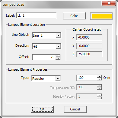
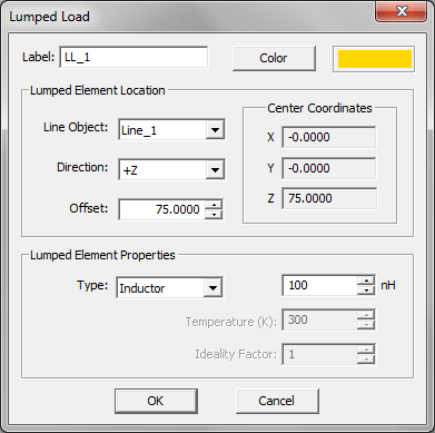
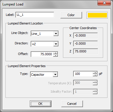
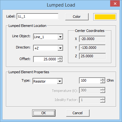
- 4.9 Lumped Loads
- 4.10 Sources & Loads For Antenna Arrays
- 4.11 Plane Waves
- 4.12 Focused Gaussian Beams
- 5 Running FDTD Simulations
- 5.1 Strategy For An Accurate & Efficient FDTD Simulation
- 5.2 FDTD Observable Types
- 5.3 The FDTD Simulation Engine Settings
- 5.4 Running A Wideband FDTD Simulation
- 5.5 Waveforms & Discrete Fourier Transforms
- 5.6 Probing Fields in Time and Frequency Domains
- 5.7 Frequency-Domain Near Field Visualization
- 5.8 Visualizing Field Evolution in Time Domain
- 5.9 Scattering Parameters and Port Characteristics
- 5.10 Far Field Calculations in FDTD
- 5.11 Defining The Far Field Box
- 5.12 Visualizing 3D Radiation Patterns
- 5.13 2D Radiation Graphs
- 5.14 Radiation Pattern Above A Half-Space Medium
- 5.15 Radar Cross Section
- 5.16 Running Frequency & Angular Sweeps
- 5.17 Defining Custom Output Parameters
- 5.18 Running A Parametric Sweep
- 5.19 3D Near & Far Field Animation
- 5.20 Running An Optimization With FDTD Simulator
- 6 Modeling 3D Periodic Structures Using FDTD
An FDTD Modeling Primer
In the Finite Difference Time Domain (FDTD) method, a discretized form of Maxwell’s equations is solved numerically and simultaneously in both the 3D space and time. During this process, the electric and magnetic fields are computed everywhere in the computational domain and as a function of time starting at t = 0. From knowledge of the primary fields in space and time, one can compute other secondary quantities including frequency domain characteristics like scattering parameters, input impedance, far field radiation patterns, radar cross section, etc.
A time domain simulation like FDTD offers several advantages over a frequency domain simulation. In certain applications, you may seek the time domain signature or behavior of a system. For example, the transient response of a circuit or an antenna might be of primary interest. In other applications, you may need to determine in the wideband frequency response of a system. In such cases, using a frequency domain technique, you have to run the simulation engine many times to adequately sample the specified frequency range. By contrast, using the FDTD method requires a single-run simulation. The temporal field data are transformed into the Fourier domain to obtain the wideband frequency response of the simulated system. Among other advantages of the FDTD method is its versatility in handling complex geometries and inhomogeneous material compositions as well as its superb numerical stability. It is worth noting that unlike frequency domain methods like the finite element method (FEM) or method of moments (MoM), the FDTD technique does not involve numerical solution of large ill-conditioned matrix equations that are often very sensitive to the mesh quality.
Like every numerical technique, the FDTD method has disadvantages, too. Adding the fourth dimension, time, to the computations increases the size of the numerical problem significantly. Unfortunately, this translates to both larger memory capacity requirements and longer computation times. Note that the field data are generated in both the 3D space and time. EM.Cube's FDTD Module uses a staircase "Yee" mesh to discretize the physical structure. This works perfectly well for rectangular objects that are oriented along the three principal axes. Difficulties start to appear for highly curved structures or slanted surfaces and lines. As a result, the quantization effect might compromise the geometrical fidelity of your structure. EM.Cube provides a default adaptive FDTD mesher that can capture the fine details of geometric contours, slanted thin layers, surfaces, etc. to arbitrary precision. However, due to the stability criterion, smaller mesh cells lead to smaller time steps, hence longer computation times. Another disadvantage of the FDTD technique compared to naturally open-boundary methods like MoM is its finite-extent computational domain. This means that to model open boundary problems like radiation or scattering, absorbing boundary conditions are needed to dissipate the incident waves at the walls of the computational domain and prevent them from reflecting back into the domain. The accuracy of the FDTD simulation results depends on the quality of these absorbers and their distance from the actual physical structure. EM.Cube's FDTD Module provides high quality perfectly match layer (PML) terminations at the boundaries, which can be placed only a quarter wavelength or less from your physical structure.
The simulated structure in FDTD usually consists of a number of objects that may have different material properties. EM.Cube’s FDTD Module categorizes objects by their material composition. Several material types are currently offered: Perfect Electric Conductor (PEC), Perfect Magnetic Conductor (PMC), Isotropic & Homogeneous Dielectric, Uniaxial Anisotropic, Full Anisotropic, and three types of dispersive materials: Debye, Drude and Lorentz.
Basics of Yee Discretization
Since FDTD is a finite domain numerical technique, the computational domain of the problem must be truncated. At the boundaries of the computational domain, proper boundary conditions must be enforced. In a shielded structure, all objects are enclosed within a perfect electric (or magnetic) conductor box. In an open boundary problem like an antenna, some kind of absorbing boundary conditions such as a perfectly matched layer (PML) must be used to emulate the free space.
The computational domain is discretized using an appropriate meshing scheme. EM.Cube uses a non-uniform, variable, staircase (pixelated) Yee mesh with a mesh density that you can customize. A fixed-cell mesh generator is also available, where you can set constant cell dimensions along the three principal axes for the entire computational domain. The variable mesh density is specified in terms of the effective wavelength inside material media. As a result, the mesh resolution and average mesh cell size differ in regions that are filled with different types of material. EM.Cube's non-uniform mesher generates more cells in the areas that are occupied by dielectric materials, fewer cells in the free space regions and no cells inside (impenetrable) PEC regions. FDTD Module's default "adaptive" mesh generator also refines the mesh around curved segments of lines, surface or solids to produce a far more accurate representation of your geometry. The example below illustrates a dielectric ellipsoid and a 3D view of its Yee mesh:
Figure 1: A dielectric object and its Yee mesh in FDTD Module.
Differential Form of Maxwell's Equations
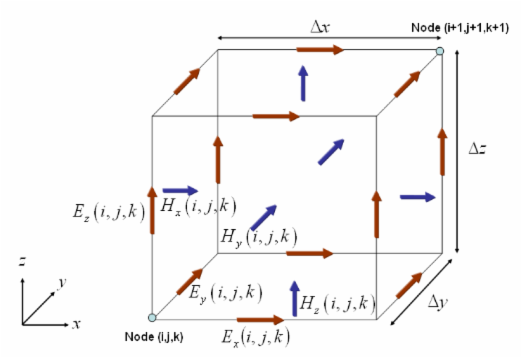
The differential form of Maxwell’s equations are solved numerically using a time marching finite difference scheme inside all the Yee grid cells. The following illustration shows the field components in the Yee grid.
Figure 1: The Yee cell geometry and definition of the electric and magnetic field components.
For example, Maxwell’s equations for an isotropic, time-invariant and homogeneous medium without electric or magnetic losses are given by:
- [math]\dfrac{\delta \mathbf{H}}{\delta t} = -\dfrac{1}{\mu} \Delta \times \mathbf{E}[/math]
- [math]\dfrac{\delta \mathbf{E}}{\delta t} = -\dfrac{1}{\epsilon} \Delta \times \mathbf{H}[/math]
where E and H are the electric and magnetic fields, respectively, ε is the permittivity and μ is the permeability. Both time- and space-derivatives are approximated with central finite differences. This results in six differential equations, one for each field component. For the field components in x-direction, the field equations result in:
- [math] H_x^{n+\frac{1}{2}} (i,j,k) = H_x^{n-\frac{1}{2}} (i,j,k) + \frac{\Delta t}{\mu (i,j,k)} \left[ \frac{E_{y}^{n}(i,j,k+1) - E_{y}^{n}(i,j,k)}{\Delta z} - \frac{E_{z}^{n} (i,j+1,k)-E_{z}^{n} (i,j,k)}{\Delta y} \right] [/math]
- [math] {E_{x}^{n+1} (i,j,k) = E_{x}^{n} (i,j,k)} + \frac{\Delta t}{\epsilon (i,j,k)} \left[ \frac{H_{z}^{n+\frac{1}{2} } (i,j,k) - H_{z}^{n+\frac{1}{2} } (i,j-1,k)}{\Delta y} - \frac{H_{y}^{n+\frac{1}{2} } (i,j,k) - H_{y}^{n+\frac{1}{2} } (i,j,k-1)}{\Delta z} \right] [/math]
where i, j, k are the grid position indices along the X, Y, Z axes and n is the current time step. Similar expressions are obtained for the Y and Z components of the electric and magnetic fields. When your physical structure involves lossy materials with nonzero electric conductivity σ and/or nonzero electric conductivity σm, the above update equations become more complicated. In the case of anisotropic materials with tensorial constitutive parameters, the electric displacement vector D and magnetic induction vector B need to be involved in the update of Maxwell's equations at every time step. This results in a total of twelve update equations at every time step. In the case of dispersive materials with time-varying constitutive parameters, additional auxiliary differential equations are invoked and updated at every time step. Applying the proper boundary conditions for all the materials inside the computational domain and at the boundaries of the domain itself, EM.Cube calculates and "updates" all the necessary field components at every mesh node, at every time step. The time marching loop continues in this way until it is terminated based on a certain criterion.
Waveform, Bandwidth & Stability
The FDTD method provides a wideband simulation of your physical structure. Frequency domain techniques often require a tedious frequency sweep to calculate the port characteristics (S/Y/Z parameters). By contrast, EM.Cube's FDTD Module performs a discrete Fourier transform (DFT) of the time domain data to calculate these characteristics at the end of a single FDTD simulation run. In order to produce sufficient spectral information, an appropriate wideband temporal waveform is needed to excite the physical structure. The general form of EM.Cube's default excitation waveform is a Modulated Gaussian Pulse given by:
- [math] E_j^{inc}(r,t)=E_0(r) \exp \left(-\frac{(t-t_0)^2}{\tau ^2} \right) \cos \left(2\pi f_0 (t-t_0)-\Phi \right),\quad j=x,y,z [/math]
where f0 is the center frequency, t0 is the time delay, t is the Gaussian pulse width, and Φ is a constant phase. In the limits, the above waveform can be reduced either to a simple Gaussian pulse:
- [math] E_j^{inc}(r,t) = E_0(r) \exp \left(-\frac{(t-t_0)^2}{\tau ^2} \right),\quad j=x,y,z [/math]
or to a continuous, single-tone, sinusoidal waveform with a frequency of f0:
- [math] E_j^{inc}(r,t) = E_{0} (r)\cos (2\pi f_0 (t-t_0)-\Phi),\quad j=x,y,z [/math]
The choice of the waveform, its bandwidth and time delay are important for the convergence behavior of the FDTD time marching loop. By default, EM.Cube uses a modulated Gaussian waveform with optimal parameters: t = 0.966/Δf and t0 = 4.5t, where Δf is the specified bandwidth of the simulation. The time delay t0 is chosen so that the temporal waveform has an almost zero value at t = 0. Of the above waveforms, modulated Gaussian and sinusoidal waveforms are band pass with no DC content, while the Gaussian pulse is low pass with a frequency spectrum that is concentrated around f = 0. In a typical FDTD simulation, you set a center frequency for the structure of interest and then specify a bandwidth around this center frequency. These together determine the lowest and highest spectral contents of your FDTD waveform. Note that setting a bandwidth equal to 2f0 sets the lowest frequency to DC (fmin = 0), which you may want to avoid in certain applications. On the other hand, using a Gaussian pulse waveform, you do want to set Δf = 2f0. In contrast to the wideband, exponentially decaying, Gaussian pulse and modulated Gaussian waveforms, the sinusoidal waveform is extremely narrowband and single-frequency indeed. It does not decay over time and continues to oscillate indefinitely after reaching a steady state.
Another issue of concern in an FDTD simulation is the numerical stability of the time marching scheme. You can set the mesh grid cell size to any fraction of a wavelength. Normally, you would expect to get better and more accurate results if you increase the mesh resolution. However, the time step is inversely proportional to the maximum grid cell size in order to satisfy the Courant-Friedrichs-Levy (CFL) stability condition:
- [math] \Delta t \le \frac{K_{CFL}} {c\sqrt{\left(\dfrac{1}{\Delta x_{min}} \right)^2 + \left(\dfrac{1}{\Delta y_{min}} \right)^2 + \left(\dfrac{1}{\Delta z_{min}} \right)^2 } } [/math]
where c is the speed of light, and KCFL is a constant. EM.Cube uses a default value of KCFL = 0.9. For a uniform grid with equal cell dimensions along the X, Y and Z directions, i.e. Δx = Δy = Δz = Δ, and the CFL condition reduces to:
- [math] \Delta t \le K_{CFL} \frac{\Delta}{\sqrt{3}c}[/math]
As can be seen from the above criterion, a high resolution mesh requires a smaller time step. Since you need to let the fields in the computational domain fully evolve over time, a smaller time step will require a larger number of time steps to achieve convergence. EM.Cube automatically chooses a time step that satisfies the CFL condition.
Perfectly Matched Layer Termination
The FDTD simulation time depends directly on the size of the computational domain. For free space radiation or scattering problems, the computational domain must be extended to infinity, which means an infinite number of cells in the computational domain. The solution to this problem is to truncate the domain by a set of artificial boundaries at a certain distance from the objects in the computational domain. The absorbing boundaries should be such that the field propagates through them without any back reflection. Different methods have been used to simulate an absorbing boundary condition in FDTD simulations. The most common ones are Mur, Liao, and the perfectly match layer (PML). The Mur boundary condition calculates the boundary field values from the three dimensional scalar wave equations, while the Liao boundary condition is based on extrapolation of the fields in space and time. In 1994, Berenger proposed a new boundary condition called the perfectly matched layer (PML), which provides a much better performance than the Liao and Mur boundary conditions. The PML medium properties surrounding the computational domain are chosen to effectively absorb all the outgoing waves propagating towards the boundaries. In PML regions, an artificial conductivity is introduced such that it starts with very small values at the free space-PML interfaces and gradually increases until it reaches its maximum value at the last layer of the PML region.
The PML boundary condition is not effective in absorbing evanescent waves, and it suffers from late-time reflections when simulating fields with very long time signatures. This is partly due to the weakly causal nature of the PML. A strictly causal form of the PML, known as the complex frequency-shifted PML (CFS-PML), was later developed by simply shifting the frequency dependent pole off the real axis and into the negative-imaginary half of the complex plane. It has been shown that the CFS-PML is highly effective at absorbing evanescent waves and signals with a long time signature. Therefore, using the CFS-PML, the boundaries can be placed closer to the objects in the computational domain, and considerable time and memory savings can be achieved. The convolutional PML (CPML) is an efficient implementation of the CFS-PML based on a stretched coordinate formulation in conjunction with recursive convolution. It has been shown that CPML requires only two auxiliary variables per discrete field point and absorbs waves in isotropic, homogeneous, inhomogeneous, lossy, dispersive, anisotropic or non-linear media without any further generalization.
The CPML is formulated in the stretched coordinate space. The CPML layers are assumed to terminate the FDTD computational domain. The X components of Maxwell's frequency-domain curl equations can then be written in the following form:
- [math] (j\omega\epsilon_x + \sigma_{ex})\tilde{E}_x = \frac{1}{s_{ey}} \frac{\partial \tilde{H}_z}{\partial y} - \frac{1}{s_{ez}} \frac{\partial \tilde{H}_y}{\partial z} [/math]
- [math] (j\omega\mu_x + \sigma_{mx}) \tilde{H}_x = -\frac{1}{s_{my}} \frac{\partial \tilde{E}_z}{\partial y} + \frac{1}{s_{mz}} \frac{\partial \tilde{E}_y}{\partial z} [/math]
where sei and smi are the stretched coordinate metrics defined by:
- [math] s_{ei} = \kappa_{ei} + \frac{\sigma_{ei}}{\alpha_{ei} + j\omega\varepsilon_0}, \quad i=x,y,z [/math]
- [math] s_{mi} = \kappa_{mi} + \frac{\sigma_{mi}}{\alpha_{mi} + j\omega\mu_0}, \quad i=x,y,z [/math]
sei and smi are the anisotropic components of the synthesized electric and magnetic conductivities in the CPML region. κei , κmi, αei and αmi are all assumed to be positive real and κei, κmi ≥ 1. Similar equations hold for the Y and Z components of the electric and magnetic fields in the CPML layers. The requirement for zero reflection at PML-PML interfaces imposes the following condition:
- [math] s_{ei} = s_{mi} \quad \Rightarrow \quad \kappa_{ei} = \kappa_{mi} ,\quad \frac{\sigma_{ei}}{\varepsilon_0} = \frac{\sigma _{mi}}{\mu_0}, \quad \frac{\alpha_{ei}}{\varepsilon_0} = \frac{\alpha_{mi}}{\mu _0} [/math]
The tilde notation above denotes the Fourier transform of the field components in the frequency domain. Transforming the above equations back to the time domain, one encounters convolution on the right hand side due to the frequency dependence of the stretched coordinate metrics:
- [math] \left(\varepsilon_x \frac{\partial E_x}{\partial t} + \sigma_{ex}E_x \right) = \breve{s}_{ey}(t) \frac{\partial H_z}{\partial y} - \breve{s}_{ez}(t)\frac{\partial H_y}{\partial z} [/math]
- [math] \left(\mu_x \frac{\partial H_x}{\partial t} + \sigma_{mx}H_x \right) = -\breve{s}_{my}(t)\frac{\partial E_z}{\partial y} + \breve{s}_{mz}(t)\frac{\partial E_y}{\partial z} [/math]
where šei(t) and šmi(t) denote functions of time that are indeed the inverse Laplace transform of sei-1 and smi-1,respectively, given by:
- [math] \breve{s}_{ei}(t) = \frac{\delta(t)}{\kappa_{ei}} - \frac{\sigma_{ei}}{\kappa_{ei}^2} u(t)\exp \left[-\left(\frac{\sigma_{ei}}{\kappa_{ei}} + \alpha_{ei} \right)\frac{t}{\varepsilon_0} \right] [/math]
- [math] \breve{s}_{mi}(t) = \frac{\delta(t)}{\kappa_{mi}} - \frac{\sigma_{mi}}{\kappa_{mi}^2} u(t)\exp \left[-\left(\frac{\sigma_{mi}}{\kappa_{mi}} + \alpha_{mi} \right)\frac{t}{\mu_0} \right] [/math]
where d(t) and u(t) denote the Dirac delta and unit step functions, respectively. The convolutions on the right hand side of the time domain equations can be accelerated by the use of the recursive convolution (RC) method.
The CPML parameters are chosen to be an increasing function of the distance from the boundaries of the computational domain. EM.Cube uses a polynomial profile of degree nPML. Given the interrelationships among these parameters, one can write:
- [math] \sigma_{ei}(r) = \frac{\varepsilon_0}{\mu_0}\sigma_{mi}(r) = \sigma_{max}\left( \dfrac{r}{\delta} \right)^{n_{PML}} [/math]
- [math] \kappa_{ei}(r) = \kappa_{mi}(r) = 1 + \left( \kappa_{max} - 1 \right) \left( \dfrac{r}{\delta} \right)^{n_{PML} } [/math]
- [math] \alpha_{ei}(r) = \frac{\varepsilon_0}{\mu_0} \alpha_{mi}(r) = \alpha _{min} + \left(\alpha_{max } - \alpha_{min } \right) \left( \frac{r}{\delta} \right)^{n_{PML}} [/math]
where r is the distance of field observation point inside the CPML layer from the edge of the computational domain. The parameters σmax, κmax, αmin and αmax as well as nPML can be modified by the user.
Time Domain Simulation Of Periodic Structures
A periodic structure is one that repeats itself infinitely in one, two or three directions. EM.Cube's FDTD Module allows you to simulate doubly periodic structures with periodicities along the X and Y directions. Many interesting structures such as frequency selective surfaces (FSS), electromagnetic band-gap (EBG) structures and metamaterial structures can be modeled using periodic geometries. In the case of an infinitely extended periodic structure, it is sufficient to analyze only a unit cell. In the FDTD method, this is accomplished by applying periodic boundary conditions (PBC) at the side walls of the computational domain. The application of the PBC is straightforward for the case of a normally incident plane wave source since the fields do not experience any delay as they travel across the unit cell. Obliquely incident plane waves, on the other hand, cause a time delay in the transverse plane. This delay requires knowledge of the future values of the fields at any time step.
A number of techniques have been proposed to solve this problem. EM.Cube uses a recently developed novel technique that is known as Direct Spectral FDTD or Constant Transverse Wavenumber method. In this technique, the components of the transverse (horizontal) wavenumber are kept constant in the direction of periodicity. This technique shows a significant advantage over the other methods for simulation of the incident illuminations close to the grazing angles.
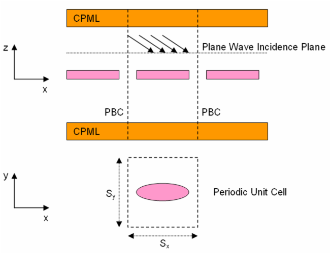
Figure 1: Diagram of a periodic structure illuminated by an obliquely incident plane wave in FDTD Module.
The figure above shows a doubly periodic structure with periods Sx and Sy along the X and Y directions, respectively. The computational domain is terminated with PBC in both X and Y directions. Along the positive and negative Z directions, it is terminated with CPML layers. Bear in mind that the PBC is also applied to the CPML layers. The computational domain is excited by a TMz or TEz plane wave incident at z = z0. The plane wave incidence angles are denoted by θ (elevation) and φ (azimuth) in the spherical coordinate system. The constant wavenumber components kx and ky in this case are defined as:
- [math]k_x = k_0 \sin\theta\cos\phi[/math]
- [math]k_y = k_0 \sin\theta \sin\phi[/math]
where [math]k_0 = \omega/c = 2\pi f/c = 2\pi/\lambda_0[/math] is the free space propagation constant, f is the operational frequency, ω is the angular frequency, λ0 is the free space wavelength, c is the speed of light in the free space. The constant transverse wavenumber kl is then given by:
- [math] k_l = \sqrt{k_x^2 + k_y^2} = k_0\sin\theta [/math]
which depends only on θ and not on φ. On the excitation plane, the incident field adopts a modulated Gaussian waveform and a complex phase delay along the periodicity direction with the following form:
- [math] H_x^{inc}(x,y,t) = -\frac{1}{\eta_0} \sin\phi \; \exp \left(-\frac{(t-t_0)^2}{\tau^2} \right) \exp(j2\pi f_0 t) \exp(-jk_x x) \exp(-jk_y y)[/math]
- [math] H_y^{inc}(x,y,t) = \frac{1}{\eta_0} \cos\phi \; \exp \left(-\frac{(t-t_0)^2}{\tau^2} \right) \exp(j2\pi f_0 t) \exp(-jk_x x) \exp(-jk_y y)[/math]
for TMz polarization and
- [math] E_x^{inc}(x,y,t) = \sin\phi \; \exp \left(-\frac{(t-t_0)^2}{\tau^2} \right) \exp(j2\pi f_0 t) \exp(-jk_x x) \exp(-jk_y y)[/math]
- [math] E_y^{inc}(x,y,t) = -\cos\phi \; \exp \left(-\frac{(t-t_0)^2}{\tau^2} \right) \exp(j2\pi f_0 t) \exp(-jk_x x) \exp(-jk_y y)[/math]
for TEz polarization. Here, f0 is the center frequency of the modulated Gaussian pulse waveform, t0 is the time delay, and τ is the Gaussian pulse width. The choices of the Gaussian waveform parameters are very critical in order to avoid possible resonances. For a fixed value of kl, the horizontal resonance occurs at:
- [math] f_{res} = \frac{k_l c}{2 \pi} [/math]
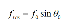
For a fixed frequency [math]f_0[/math] and a fixed incidence angle [math]\theta_0[/math], the resonant frequency is reduced to:
The modulated Gaussian waveform must be chosen such that its effective bandwidth avoids the horizontal resonant frequency. Otherwise, the temporal response of the structure starts to oscillate, and the time marching loop will not converge. To avoid this problem, the modulation frequency and bandwidth of the waveform are chosen to satisfy the following condition:
- [math] f_{mod} \ge f_{res} + \dfrac{1}{2}\Delta f = \dfrac{k_{l,fixed}\;c}{2\pi} + \dfrac{1}{2}\Delta f [/math]
Defining The Physical Structure
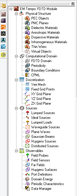
In EM.Cube's FDTD Module, a physical structure consists of one or several objects that are grouped and identified by their material types. Materials are divided into five categories that are listed under the Physical Structure node at the top of the Navigation Tree:
Under each material node, you can create new material groups of the same type/category but with different properties (color, texture, or electric and magnetic constitutive parameters). These material groups are used to organize the CAD objects that you draw in the project workspace or import from external model files. When you create a new geometrical object such as a Box or a Sphere, it is inserted under the currently active material type. There is only one material group that is active at any time. It is normally recommended that you first create material groups, and then draw new objects as part of the currently active material group. However, if you start a new FDTD Module project from scratch, and you start drawing a new object without having previously defined any material groups, a new default PEC group is created and added to the Navigation Tree to hold your new CAD object.
Figure 1: FDTD Module's Navigation Tree.
Perfect Conductors
EM.Cube's FDTD Module offers two types of perfect conductors:
- Perfect Electric Conductor (PEC): The tangential electric field on the surface of this type of perfect conductor is zero. The electric and magnetic fields are assumed to vanish inside the volume of a PEC object. A PEC material is characterized by an infinite electric conductivity (σ = ∞).
- Perfect Magnetic Conductor (PMC): The tangential magnetic field on the surface of this type of perfect conductor is zero. The electric and magnetic fields are assumed to vanish inside the volume of a PMC object. A PMC material is characterized by an infinite magnetic conductivity (σm = ∞).
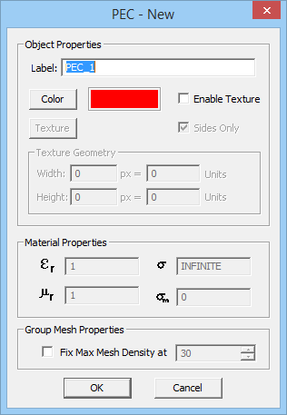
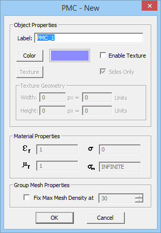
PEC and PMC materials do not have any constitutive material properties that you can modify except for their color or texture. Note that FDTD Module's PMC materials are different in nature than the PMC traces you will find in EM.Cube's Planar Module. In the latter, the PMC term is applied to slot traces, which represent finite-sized cut-out objects (areas) from an infinite horizontal PEC ground plane. FDTD Module's PMC objects, by contrast, can be arbitrarily oriented surface objects or impenetrable solid objects of finite extents.
To define a new PEC or PMC material, follow these steps:
- Right click on either the PEC or PMC items in Navigation Tree and select Insert New PEC/PMC... from the contextual menu.
- Specify a Label and Color (and optional Texture) for the PEC or PMC material being created.
- Click the OK button of the dialog to accept the changes and close it.
Once a PEC or PMC node has been created on the Navigation Tree, you can draw objects in the project workspace, and they will be added under that node. In other words, all the CAD objects belonging to a PEC or PMC group have the same color or texture.
Figure 1: FDTD Module's PEC and PMC material dialogs.
Dielectric Materials
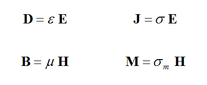
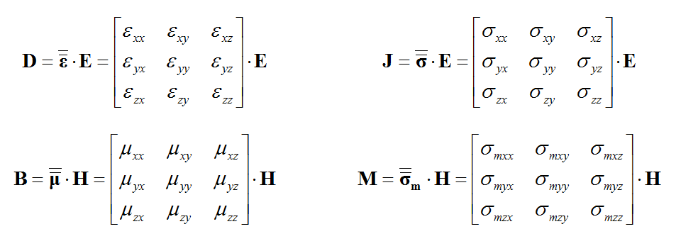
In EM.Cube's FDTD Module, a dielectric material represents a general isotropic material with both electric and magnetic properties. The constitutive parameters of a dielectric material include permittivity (ε), permeability (μ), electric conductivity (σ) and magnetic conductivity (σm):
where E and H are the electric and magnetic fields, respectively, D is the electric flux density, also known as the electric displacement vector, B is the magnetic flux density, also known as the magnetic induction vector, and J and M are the electric and magnetic current densities, respectively. For example, an imperfect metal can be represented by a dielectric material that has a large, finite, electric conductivity. PEC and PMC, therefore, are the limiting cases of an isotropic dielectric material when σ → ∞ or σm → ∞, respectively.
To define a new Dielectric material, follow these steps:
- Right click on the Dielectric item of the Navigation Tree and select Insert New Dielectric... from the contextual menu.
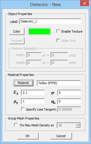
- Specify a Label, Color (and optional Texture) and the electromagnetic properties of the dielectric material to be created: Relative Permittivity (εr), Relative Permeability (μr), Electric Conductivity (σ) and Magnetic Conductivity (σm).
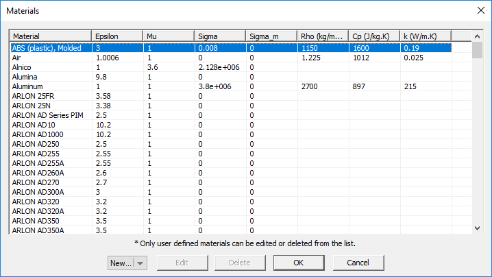
- You may also choose from a list of preloaded material types. Click the button labeled Material to open EM.Cube's Material List dialog. Select the desired material from the list or type the first letter of a material to find it. For example, typing V selects Vacuum in the list. Once you close the dialog by clicking OK, the selected material properties fill the parameter fields automatically.
- Click the OK button of the dielectric material dialog to accept the changes and close it.
Figure 1: FDTD Module's Dielectric Material dialog.
Figure 2: EM.Cube's material list.
Anisotropic Materials

EM.Cube's FDTD Module allows you to define a general anisotropic material, whose constitutive parameters, i.e. permittivity (ε), permeability (μ), electrical conductivity (σ) and magnetic conductivity (σm), are all tensorial in nature. Each constitutive parameter in this case is represented by a 3×3 matrix:
A "Uniaxial" material is a special case of an anisotropic material whose constitutive parameters are all diagonal matrices. Specifying an anisotropic material as Uniaxial in the FDTD Module has a very important computational implication. There are six field update equations for uniaxial materials at each time steps: three for the electric field and three for the magnetic field. In this respect, a uniaxial material is similar to an isotropic dielectric material. On the other hand, a fully anisotropic material with non-zero off-diagonal constitutive matrix elements requires twelve update equations at each time step: three equations for the three components of each of the four vector fields E, D, H and B. As a result, the time loop for fully anisotropic materials takes much longer time than uniaxial materials.
To define a new Anisotropic material, follow these steps:
- Right click on the Anisotropic item of the Navigation Tree and select Insert New Anisotropic... from the contextual menu.
- Specify a Label and Color (and optional Texture) for the anisotropic material being created.
- By default, the box labeled Uniaxial Material is checked. This means that all the constitutive matrices are diagonal. The off-diagonal elements of ε, μ, σ and σm matrices are all set to zero and greyed out. You need to enter values for the diagonal elements of these matrices. To set values for the off-diagonal elements of the constitutive matrices, you have to remove the "Anisotropic" check mark first.
- Click the OK button of the dialog to accept the changes and close it.
Dispersive Materials
PEC, PMC, dielectric and anisotropic materials are non-dispersive. In other words, their constitutive parameters do not vary with frequency. Most of the materials used in the design of RF and microwave circuits, antennas and systems fall into this frequency-independent category. However, there are other types of materials whose constitutive parameters exhibit frequency-dependent behaviors. EM.Cube's FDTD Module currently offers three types of dispersive material:
- Debye Material
- Drude Material (Unmagnetized Plasma)
- Lorentz Material
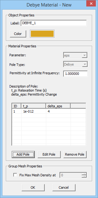
The FDTD simulation engine uses the Auxiliary Differential Equation (ADE) method to model dispersive materials. EM.Cube allows you to define an arbitrary number of poles for each of the above dispersive material types. Keep in mind that all the objects belonging to the same dispersive material group have the same dispersion properties.
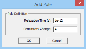
The complex permittivity of a Debye material with N poles is given by:
- [math] \varepsilon (\omega) = \varepsilon_\infty + \sum_{p=1}^N \dfrac{\Delta \varepsilon_p}{1 + j\omega \tau_p}, \quad \Delta \varepsilon_p = \varepsilon_{sp} - \varepsilon_\infty [/math]
where [math]\varepsilon_{\infty}[/math] is the value of the permittivity at infinite frequency, [math]\tau_p[/math] is the relaxation time corresponding to the pth pole having the unit of seconds, and [math]\varepsilon_{sp}[/math] is the value of the static permittivity (at DC) corresponding to the pth pole. [math]\Delta \varepsilon_p = \varepsilon_{sp} - \varepsilon_{\infty}[/math] represents the change in permittivity due to the pth pole.
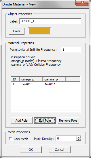
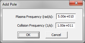
Unmagnetized plasmas are typically modeled as Drude materials. The complex permittivity of a Drude material with N poles is given by:
- [math] \varepsilon(\omega) = \varepsilon_{\infty} - \sum_{p=1}^N \dfrac{{\omega_p}^2}{\omega^2 - j\omega \nu_p} [/math]
where [math]\omega_p[/math] and [math]\nu_p[/math] are the angular plasma frequency and angular collision frequency corresponding to the pth pole, respectively, and both are expressed in rad/s. For an unmagnetized plasma, [math]\varepsilon_{\infty} = 1[/math].
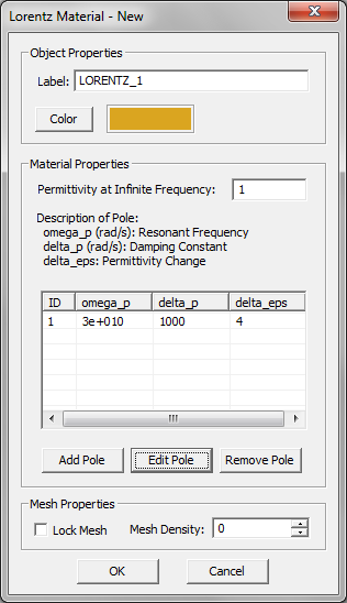
The complex permittivity of a Lorentz material with N poles is given by:
- [math] \varepsilon(\omega) = \varepsilon_{\infty} - \sum_{p=1}^N \dfrac{\Delta \varepsilon_p {\omega_p}^2}{\omega^2 - 2j\omega \delta_p - {\omega_p}^2}, \quad \Delta \varepsilon_p = \varepsilon_{sp} - \varepsilon_{\infty} [/math]
where [math]\omega _p[/math] and [math]\delta_p[/math] are the angular resonant frequency and angular damping frequency corresponding to the pth pole, respectively, and both are expressed in rad/s. Similar to a Debye material, [math]\Delta \varepsilon_p = \varepsilon_{sp} - \varepsilon_{\infty}[/math] represents the change in permittivity due to the pth pole.
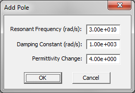
Figure 1: FDTD Module's Debye, Drude and Lorentz Material dialogs and their respective "Add Pole" dialogs.
Geometrical Rules & Material Hierarchy
The following rules apply to the definition of materials and objects in EM.Cube's FDTD Module:
- Under the PEC and PMC material categories, you can define all types of solid and surface objects.
- Under the Dielectric, Anisotropic and Dispersive material categories, you can define only solid objects.
- Under the PEC material category, you can also define curve objects such as lines, polylines, etc. to model wire structures.
EM.Cube's FDTD Module allows overlapping objects, although it is generally recommended that object overlaps be avoided in favor of clearly defined geometries and object boundaries. If two or more objects of the same material type and group overlap, they are merged using the Boolean union operation during the mesh generation process.
If two overlapping objects belong to two different material categories, then the material properties of the FDTD cells in the overlap region will follow the FDTD Module's material priority rule. In that case, the overlap area cells will always be regarded as having the material type of the higher priority. According to this rule, the material types are ordered from the highest priority to the lowest in the following manner:
- PEC
- PMC
- Dispersive
- General Anisotropic
- Uniaxial Anisotropic
- Dielectric
It is therefore recommended to avoid overlapping objects belonging to different material groups within the same material category. To overlap two PEC objects with different colors does not matter. But to overlap two dielectric solids with different permittivity will create ambiguity. In that case, the FDTD simulation will run and complete successfully, but you will not be clear as to which permittivity value was used for the cells of the overlap region.
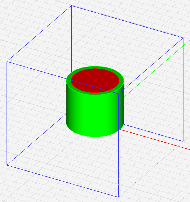
Sometimes taking advantage of FDTD Module's material priority rule makes construction of complex objects easier. For example, a dielectric coated metallic cylinder can be modeled by two concentric cylinders: an inner PEC of smaller radius and an outer dielectric of larger radius as shown in the illustration below. The portion of the dielectric cylinder that overlaps the inner PEC cylinder is ignored by the FDTD engine because the PEC cylinder takes precedence over the dielectric in the material hierarchy. Alternatively, you can model the same structure by an inner solid PEC cylinder enclosed by an outer hollow pipe-shaped dielectric cylinder. The hollow solid can be built by extruding a planar ring or by subtracting two concentric cylinders. The first configuration utilizing material hierarchy is, of course, much easier to construct.
Figure 1: Geometric construction of a dielectric-coated metallic cylinder.
Moving Objects Among Material Groups
If two or more material groups are defined in the Navigation Tree, only one of them can be active. By default, the last material defined is active. When you draw new objects, they are inserted under the active material node of the Navigation Tree, which is always listed in bold letters. Any material can be made active by right clicking on its name in the Navigation Tree and selecting the Activate item of the contextual menu.
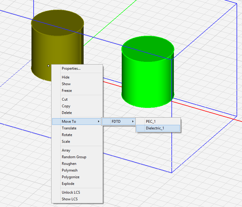
You can move one or more selected objects to any other material group. Right click on the highlighted selection and select Move To > FDTD > from the contextual menu. This opens another sub-menu with a list of all the available material groups already defined in your FDTD Module project. Select the desired material node, and all the selected objects will move to that material group. The objects can be selected either in the project workspace, or their names can be selected from the Navigation Tree. In the case of a multiple selection from the Navigation Tree using the keyboard's Shift Key or Ctrl Key, make sure that you continue to hold the keyboard's Shift Key or Ctrl Key down while selecting the "Destination" material group's name from the contextual menu.
In a similar way, you can move one or more objects from an FDTD material group to one of EM.Cube's other modules. In this case, the sub-menus of the Move To > item of the contextual menu will indicate all the EM.Cube modules that have valid groups for transfer of the selected objects. You can also move one or more objects from EM.Cube's other modules to a material group in the FDTD Module. This is especially useful when importing structure from external model files. Keep in mind that in EM.Cube you can import external objects only to CubeCAD.
Figure 1: Moving objects from one FDTD material group to another.
Computational Domain & FDTD Mesh Generation
The FDTD Solution Domain
The FDTD method solves computational electromagnetic problems within a finite region of space. Thus, a finite-extent solution domain must be defined before the problem can be solved. This is rather straightforward in the case of a shielded structure, where a typical PEC enclosure box defines the computational domain. The difficulty arises when you try to model an open-boundary structure like an antenna. In that case, the computational domain must be truncated using appropriate termination boundary conditions. For open-boundary circuit-type structures like filters, couplers, etc., without a shielding, it is still possible to place a PEC enclosure box at a distance from the actual structure. However, the distance of the box walls from the structure must be large enough to eliminate any coupling effects. Furthermore, you must also watch for spurious box resonance effects, as you effectively place your structure inside a resonant cavity. The objective of termination boundary conditions is to eliminate the reflections from the walls of the domain box back to the computational domain. The previous releases of EM.Cube featured various termination boundary conditions like absorbing boundary conditions (ABC) and uniaxial perfectly matched layer (UPML). In this release of EM.Cube's FDTD Module, we have phased out all the previous diverse boundary conditions in favor of Convolutional Perfectly Matched Layer (CPML), which has demonstrated a superior performance for a wide range of applications.
In FDTD Module, you can define two types of domain box. A "Default" type domain box is placed at a specified offset distance from the largest extents of your physical structure (global bounding box). In addition, you have two options to specify the offset distance, either in free-space wavelengths or in terms of the number of free-space grid cells. A "Custom" type domain box, on the other hand, is completely defined by you in the World Coordinate System (WCS). In this case, you have to specify the lower left front corner (Corner 1) and upper right back corner (Corner 2) of the domain box. These coordinates can be set arbitrarily, but you need to make sure that your custom domain box completely encloses your structure. When you start a new project in FDTD Module, a default-type domain is automatically created with a default offset value set equal to a quarter free-space wavelength (0.25λ0). As soon as you draw your first object, a blue domain box is placed around your object. As you add more objects and increase the overall size of your structure, the domain box grows accordingly to encompass your entire physical structure. When you delete objects from the project workspace, the domain box also shrinks accordingly.
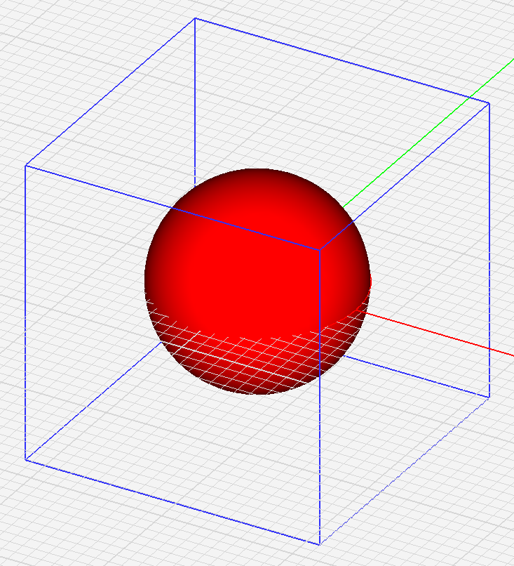
Figure 1: The computational domain box enclosing a metallic sphere.
Computational Domain Settings

To set the solution domain of your FDTD Module project, follow these steps:
- Click the Domain
 button of the Simulate Toolbar or select Menu > Simulate > Computational Domain > Domain Settings... or right click on the FDTD Domain item of the Navigation Tree and select Domain Settings... from the contextual menu, or use the keyboard shortcut Ctrl+A. The Domain Settings Dialog opens up, showing the current domain type selection.
- Select one of the two options for Domain Type: Default or Custom.
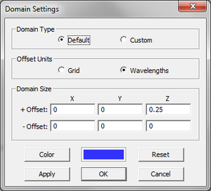
- If you select the "Default" domain type, the domain box is defined in terms of the offsets along the X, Y and Z directions from the largest extents of your physical structure. Select one of the two options for Offset Units: Grid and Wavelength. In the section titled "Domain Size", enter the amount of domain extension beyond the largest extents of the structure along the ±X, ±Y and ±Z directions. Note that in the case of a default-type domain box, the offset values based on your current project settings (frequency and units).
- When the Wavelength option is selected for Offset Units, additional free space is added around the structure by the specified ±X, ±Y and ±Z offsets in free space wavelengths. Note that the free space wavelength for this purpose is calculated at the center frequency of the project. The default value of the offset in this case is a quarter free space wavelength. Note that with this option, the number of the additional cells and their cell size is not fixed; they vary from structure to structure.
- When the Grid option is selected for Offset Units, the six offset values represent the number of additional free-space mesh cells that are placed in each direction beyond the largest bounding box around the physical structure. The default value of the offset in this case is eight grid cells along the ±X, ±Y and ±Z directions.
- If you select the "Custom" domain type instead, you need to enter values for the coordinates of the lower-left-front corner, Corner 1, and the upper-right-back corner, Corner 2, of the domain box.
- After you change values or settings, click the Apply button to make the changes effective. To recover the default values, click the Defaults button of the dialog. Click OK to save the settings and close the dialog.
By default, the domain box is shown as a wireframe box with blue lines, enclosing your structure in the project workspace. You have the option to hide or show the domain’s bounding box either by toggling the status of Menu > Simulate > Computational Domain > Show Domain Box or by right clicking the Computational Domain item of the Navigation Tree and selecting the Show or Hide item of the contextual menu and toggling their status. You can also change the color of the domain box from the Domain Settings dialog.
Domain Boundary Conditions

To solve an FDTD problem, proper boundary conditions must be enforced on the bounding walls of the solution domain. The current release of EM.Cube's FDTD Module supports four types of boundary conditions:
- PEC
- PMC
- Convolutional Perfectly Matched Layers (CPML)
- Periodic Boundary Conditions (PBC)
By default, all the six sides of the computational domain box are set to CPML, representing a completely open-boundary structure. Different boundary conditions can be assigned to each of the six sides of the domain box. The periodic boundary conditions are special ones that are assigned through FDTD Module's Periodicity Dialog and will be discussed later under modeling of periodic structures. The current release of EM.Cube allows periodic boundary conditions only on the side walls of the computational domain, and not on the top or bottom walls.
To define the boundary conditions of the solution domain, follow these steps:
- Select Menu > Simulate > Computational Domain > Boundary Conditions or right click on the Boundary Conditions item in the Computational Domain section of the Navigation Tree and select Boundary Conditions... from the contextual menu. The Boundary Conditions Dialog opens.
- You need to assign the type of boundary condition on each of the six domain boundaries: ±X, ±Y and ±Z. For each face, choose one of the three options available: PEC, PMC or PML.
The PEC and PMC boundary conditions are the most straightforward to set up and use. Assigning the PEC boundary to one of the bounding walls of the solution domain simply forces the tangential component of the electric field to vanish at all points along that wall. Similarly, assigning the PMC boundary to one of the bounding walls of the solution domain forces the tangential component of the magnetic field to vanish at all points along that wall. For planar structures with a conductor-backed substrate, you can use the PEC boundary condition to designate the bottom of the substrate (the -Z Domain Wall) as a PEC ground. For shielded waveguide structures, you can designate all the lateral walls as PEC. Similarly to model shielded cavity resonators, you designate all the six walls as PEC.
A Closer Look At CPML
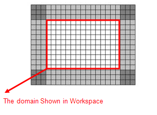
In many electromagnetic modeling problems you need a boundary that simply absorbs all the incoming radiation. For problems of this nature, an absorbing boundary condition (ABC) is often chosen that effectively minimizes wave reflections at the boundary. Usually two or more ABC layers are placed at the boundaries of the structure to maximize wave absorption. The boundary ABC cells in the project workspace are transparent to the user. But, in effect, multiple rows of ABC cells are placed on the exterior side of each face of the visible domain box.
Figure: The boundary ABC cells placed outside the visible domain box.
EM.Cube provides Perfectly Matched Layers (PML) as absorbing boundary conditions. PML's are layers of fictitious complex anisotropic materials designed to absorb any incident electromagnetic wave at all angles of incidence. The advantage of using a PML boundary condition over other types of ABC is that you do not need to care about what material or combinations of materials exist at the boundaries, since the PML can absorb anything! The disadvantage of using PML is that they require more computational resources and more sophisticated update field equations. Several types of PML have been proposed in the FDTD literature. EM.Cube's FDTD Module uses the Convolutional Perfectly Matched Layer (CPML). This is based on a newer implementation of the complex frequency-shifted PML (CFS-PML) that uses recursive convolution. It has been shown that CPML is highly effective at absorbing evanescent waves and signals with a long time signature. Therefore, using CPML, you can place the boundaries much closer to the objects in the project workspace.
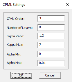
You can set the number of CPML layers as well as their order. This is done through the CPML Settings Dialog, which can be accessed by right clicking on the CPML item in the Computational Domain section of the Navigation Tree and selecting CPML Settings... from the contextual menu. By default, four CPML layers of the third order are placed outside the FDTD problem domain. It is recommended that you always try a four-layer CPML first to assess the computational efficiency. The number of CPML layers may be increased only if a very low reflection is required (<-40dB).
Figure: FDTD Module's CPML Settings dialog.
Modeling Planar Structures of Infinite Extents
You may occasionally want to use EM.Cube's FDTD simulator to model planar structures. Although EM.Cube provides the more computationally efficient Planar Module for this very purpose, there are many cases when an FDTD simulation might prove advantageous over a 2.5-D MoM simulation. Examples include examining the transient response of a planar structure, very wideband simulations, planar structures involving complex materials or 3D geometries embedded inside the substrate layers, to name a few.
A planar substrate usually consists of one or more dielectric layers, possibly with a PEC ground plane at its bottom. Unlike EM.Cube's Planar Module, where the substrate layers are defined implicitly in the "Stack-up Settings" dialog, in the finite-domain FDTD Module, you need to draw each dielectric layer separately and then stack them up manually. The substrate of a planar layered structure extends laterally to infinity. In other words, the ±X and ±Y boundary walls must, in effect, retreat to infinity. This can be accomplished in the FDTD Module by setting up the CPML layers in a particular way. For this purpose, the lateral CPML layers need to move in and touch the sides of the dielectric layer stack-up.
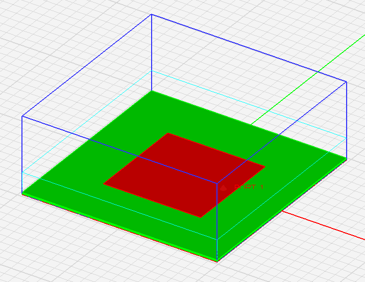
In other words, to model a laterally infinite dielectric substrate, you must assign a PML boundary condition to the four lateral sides of the domain box and set the lateral domain offset values along the ±X and ±Y directions all equal to zero. If the planar structure ends in an infinite dielectric half-space from the bottom, you must assign a PML boundary condition to the bottom side of the domain box and set the -Z offset equal to zero. Similarly, if the planar structure ends in an infinite PEC ground plane from the bottom, you must assign a PEC boundary condition to the bottom side of the domain box and set the -Z offset equal to zero.In the latter case, the presence of the metal plane at the bottom of the physical structure is implied although you will not see it in the project workspace. The CPML layers on the sides and at the bottom of the computational domain will absorb all the incident waves propagating in the free space or inside the substrate layers and thus emulate infinite extents. This leaves only the +Z offset with a nonzero value. The top CPML layer is moved back and placed above the finite parts of the structure.
| |
The current release of EM.Cube's FDTD Module does not support anisotropic or dispersive layers of laterally infinite extents. In other words, You can only define anisotropic and dispersive material objects of finite size that do not touch the CPML boundaries. |
Figure 1: Setting the ±X and ±Y and -Z domain offsets equal to zero for a laterally infinite planar structure with a PEC ground.
Creating A Yee Mesh
The mesh generation process in EM.Cube's FDTD Module involves four steps:
- Setting the mesh type, density and other properties.
- Checking the mesh grid planes.
- Generating the mesh.
- Verifying the mesh.
EM.Cube's FDTD mesh is a rectangular Yee mesh that extends to the entire computational domain. It is primarily constructed from three mesh grid profiles along the XY, YZ and ZX principal planes. These projections together create a 3D rectangular (pixelated) mesh space. You have the option to choose one of the three FDTD mesh types:
- Adaptive Mesh
- Regular Mesh
- Uniform Mesh
The default choice is the adaptive mesh, which is a quite sophisticated mesh. The resolution of the adaptive FDTD mesh is driven by the Mesh Density, expressed in cells per effective wavelength. Since FDTD is a time-domain method and the excitation waveform may have a wideband spectral content, the effective wavelength is calculated based on the highest frequency of the project: fmax = f0 + Δf/2, where f0 is your project's center frequency and Δf (or BW) is its specified bandwidth. In other words, the effective wavelength in the free space is λ0,eff = c / fmax, c being the speed of light in the free space. The adaptive FDTD mesh, however, produces different grid cell sizes in the free space regions and inside dielectric regions. The effective wavelength in a dielectric material with relative permittivity er and permeability µr is given by λd,eff = λ0,eff / √εrμr. Therefore, the average ratio of the cell size in a dielectric region to the cell size in the free space is 1/√(εrμr). The adaptive FDTD mesh generator also takes note of the geometrical features of the objects it discretizes. This is more visible in the case of curved solids, curves surfaces and curved wires or obliquely oriented planes and lines which need to be approximated using a staircase profile. The mesh resolution varies with the slope of the geometrical shapes and tries to capture the curved segments in the best way. Another important feature of the adaptive FDTD mesher is generation of gradual grid transitions between low-density and high-density mesh regions. For example, this often happens around the interface between the free space and high permittivity dielectric objects. Gradual mesh transitions provide better accuracy especially in the case of highly resonant structures.
According to the Courant-Friedrichs-Levy (CFL) stability criterion, the FDTD time step is determined by the smallest cell size in your FDTD mesh. Occasionally, FDTD Module's adaptive mesh generator may create extremely tiny grid cells that would result in extremely small time steps. This would then translate into a very long computation time. EM.Cube offers the "Regular" FDTD mesh generator, which is a simplified version of the adaptive mesh generator. In a regular FDTD mesh, the grid cell sizes stay rather the same in objects of the same material composition. The mesh resolution increases in materials of higher permittivity and/or permeability based on the effective wavelength in exactly the same way as the adaptive mesh. Finally, EM.Cube's FDTD Modules offers a "Uniform" FDTD mesh generator. The uniform mesh consists of three uniform grids along the XY, YZ and ZX principal planes. In other words, the grid cell sizes Δx, Δy and Δz are fixed throughout the entire computational domain. In this case, the uniform mesh generator has to fit your physical structure to the fixed mesh, rather than adapting the mesh to your physical structure.
Viewing The FDTD Mesh
Because a full 3D FDTD mesh is difficult to visualize everywhere in the computational domain, only the discretized objects are displayed in EM.Cube's "Mesh View" mode. In particular, only the outer boundary cells on the surface of solid objects are shown. However, you can view the mesh grid planes across the domain. You can even step these planes back and forth inside the domain and view different mesh profiles of your physical structure.
To generate an FDTD mesh and view it the project workspace, follow these steps:
- First, click the Mesh Settings
 button of the Simulate Toolbar or select Menu > Simulate > Discretization > Mesh Settings..., or right click on the Yee Mesh item of the Navigation Tree and select Mesh Settings... from the contextual menu, or use the keyboard shortcut Ctrl+G. The Mesh Settings Dialog opens up, where you can set the values of the various mesh parameters including the Mesh Density.
- After specifying the desired mesh density, you can examine the mesh grid plane. The XY, YZ, and ZX mesh grid planes can be displayed through Menu > Simulate > Discretization > Grid Planes > XY Plane, YZ Plane or ZX Plane or by right clicking on one of the three XY Plane, YZ Plane or ZX Plane items in the Discretization section of the Navigation Tree and selecting Show from the contextual menu. The mesh grid planes give you a good idea of what the mesh will look like once it is generated and its resolution along different planes. To remove a mesh grid plane from the project workspace, select Menu > Simulate > Discretization > Grid Planes > one more time and remove the check mark in front of the name of the currently displayed mesh grid plane, or right click on the name of the currently displayed mesh grid plane in the Navigation Tree and select Hide from the contextual menu.
- To display the FDTD mesh, click the Show Mesh
 button of the Simulate Toolbar or select Menu > Simulate > Discretization > Show Mesh or use the keyboard shortcut Ctrl+M. This takes EM.Cube into its "Mesh View" mode, and the Yee mesh of the whole structure is displayed in the project workspace. While the mesh view is enabled, the Show Mesh
  button remains depressed. To get back to EM.Cube's "Normal View" mode, click this button one more time, or deselect Menu > Simulate > Discretization > Show Mesh to remove its check mark or simply hit the Esc Key of the keyboard.
In EM.Cube's "Mesh View" mode, you can rotate or pan the view of the project workspace, but you cannot edit the objects. "Show Mesh" generates a new mesh and displays it if there is none in the memory, or it simply displays an existing mesh in the memory. This is a useful feature because generating an FDTD mesh may take a long time depending on the complexity of structure and the total size of the computational domain. If you change the structure or alter the mesh settings, a new mesh is always generated. You can ignore any mesh in the memory and force EM.Cube to generate a fresh FDTD mesh from the ground up by selecting Menu > Simulate >Discretization > Regenerate Mesh or by right clicking on the Yee Mesh item of the Navigation Tree and selecting Regenerate from the contextual menu.
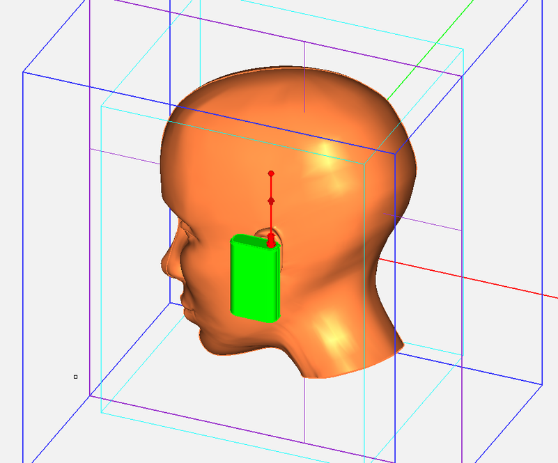
Figure 1: A human head model and a cellular phone handset on its side.
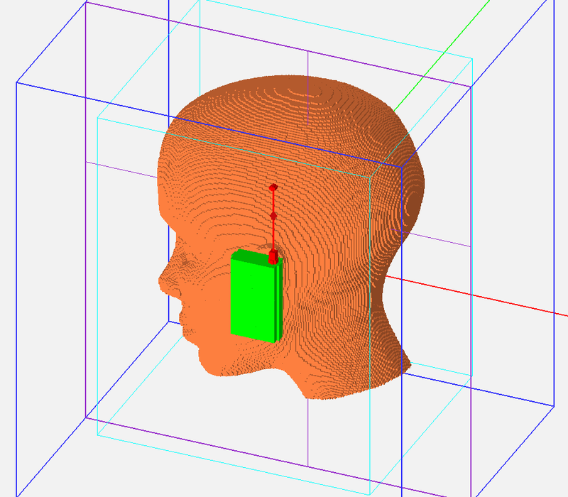
Figure 2: The regular FDTD mesh of the human head model and the cellular phone handset.
Mesh Profiling & Grid Coordinate System
A volumetric FDTD mesh is overwhelming for visualization in the 3D space. For this reason, EM.Cube's mesh view only shows the outline of the (staircased) meshed objects, skipping the outline of all the individual brick cells in the entire computational domain. The mesh grid planes provide a 2D profile of the mesh cells along the principal coordinate planes. Since the Yee cells are congruent along the coordinate axes, the three mesh grid planes together provide a complete picture of the entire FDTD mesh. To display a mesh grid planes, select Menu > Simulate > Discretization > Grid Planes > and pick one of the three options: XY Plane, YZ Plane or ZX Plane. You may also right click on one of the XY Plane, YZ Plane or ZX Plane items in the Discretization section of the Navigation Tree and select Show from the contextual menu.
While a mesh grid plane is visible, you can move it back and forth between the two boundary planes at the two opposite sides of the computational domain. You can do this in one of the following four ways:
- Using the keyboard's Page Up (PgUp) Key and Page Down (PgDn) key.
- By selecting Menu > Simulate > Discretization > Grid Planes > Increment Grid or Decrement Grid.
- By right clicking on one of the XY Plane, YZ Plane or ZX Plane items in the Discretization section of the Navigation Tree and selecting Increment Grid or Decrement Grid from the contextual menu.
- Using the keyboard shortcuts ">" or "<".
As you “step through” or profile the mesh grid, you can see how the structure is discretized along internal planes of the computational domain.
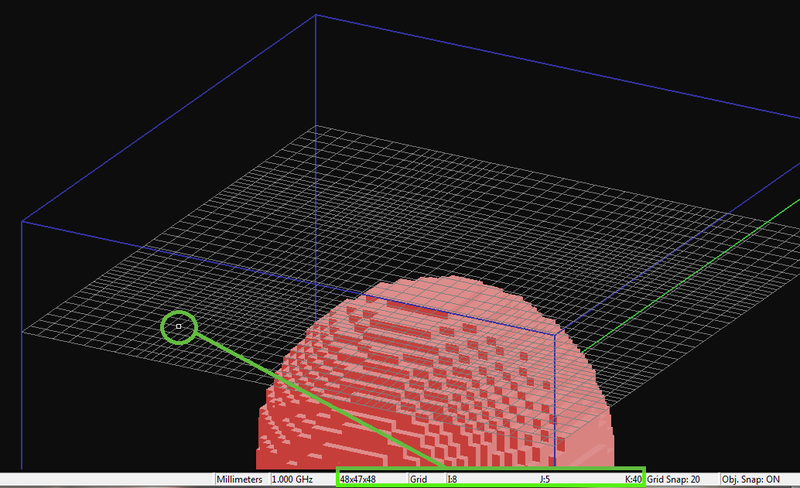
Once the project structure is meshed in EM.Cube's FDTD Module, a second coordinate system becomes available to you. The mesh grid coordinate system allows you to specify any location in the computational domain in terms of node indices on the mesh grid. EM.Cube displays the total number of mesh grid lines of an FDTD simulation domain (Nx × Ny × Nz) along the three principal axes on the Status Bar. Therefore, the number of cells in each direction is one less than the number of grid lines, i.e. (Nx-1)× (Ny-1) × (Nz-1). The minimum X, Y, and Z coordinates of the FDTD domain in the world coordinate system (Xmin, Ymin, Zmin), which represent the lower left front corner of the domain box, become the origin of the mesh grid coordinate system (0,0,0), The maximum domain coordinates, which represent the upper right back corner of the domain box, are therefore (Nx-1, Ny-1, Nz-1).
EM.Cube allows you to navigate through the mesh grid and evaluate the grid points individually. Every time you display one of the three mesh grid planes, the "Grid Coordinate System (GCS)" is automatically activated. On the Status Bar, you will see ![]() instead of the default
instead of the default ![]() . This means that the current coordinates reported on Status Bar are now expressed in grid coordinate system. The current grid point is displayed by a small white circle on the current mesh grid plane, and it always starts from (I= 0, J=0, K=0). Using the keyboard's Arrow Keys, you can move the white circle through the mesh grid plane and read the current node's (I, J, K) indices on the status bar. You can switch back to the "World Coordinate System (WCS)" or change to the "Domain Coordinate System" by double-clicking the status bar box that shows the current coordinate system and cycling through the three options. The domain coordinate system is one that establishes its origin at the lower left front corner of the computational domain and measure distances in project unit just like the WCS.
. This means that the current coordinates reported on Status Bar are now expressed in grid coordinate system. The current grid point is displayed by a small white circle on the current mesh grid plane, and it always starts from (I= 0, J=0, K=0). Using the keyboard's Arrow Keys, you can move the white circle through the mesh grid plane and read the current node's (I, J, K) indices on the status bar. You can switch back to the "World Coordinate System (WCS)" or change to the "Domain Coordinate System" by double-clicking the status bar box that shows the current coordinate system and cycling through the three options. The domain coordinate system is one that establishes its origin at the lower left front corner of the computational domain and measure distances in project unit just like the WCS.
Figure 1:The grid cursor on the XY grid plane and its grid coordinates (I, J, K) displayed on the status bar.
Meshing Arbitrary Geometries
Straight lines, boxes and rectangular plates whose edges are aligned with the three principal axes are the simplest objects to mesh in the FDTD Module. Such objects preserve their shapes exactly after discretization. All the objects with curved edges and curved surfaces or objects with straight edges and flat faces that are not parallel to the principal axes or principal planes need to be discretized using a staircase profile.
In the cases of oblique lines and slanted faces (like lateral faces of a pyramid), a uniform staircase profile is used by all of FDTD Module's three mesh generators. in other words, the cell sizes or grid line spacing remain the same across the edge or face, since the slope is constant. In the case of curved edges and curved faces or surfaces (like a sphere), the uniform and regular mesh generators use a uniform staircase profile. However, the adaptive mesh generator uses a variable staircase profile, where the cell sizes of grid line spacing vary with the curvature (derivative) of the edge or face. As a result, a higher mesh resolution is achieved at "more curvy" areas to better capture the geometrical details.
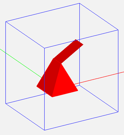
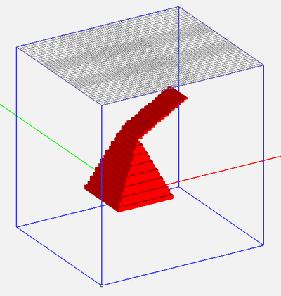
Figure 1: A pyramidal object with a slanted plate and its adaptive FDTD mesh.
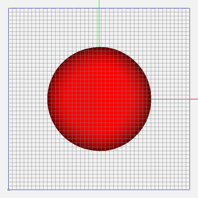
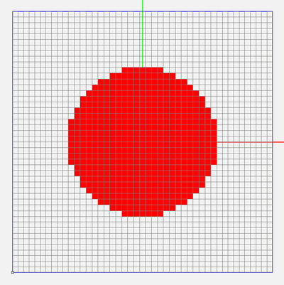
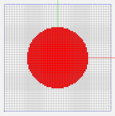
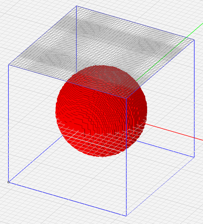
Figure 2: The geometry of a sphere and its regular and adaptive FDTD meshes (top and perspective views).
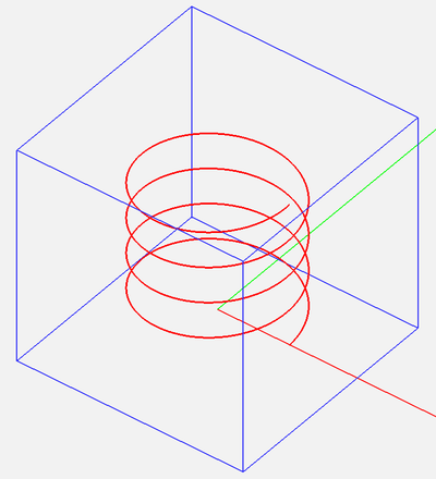
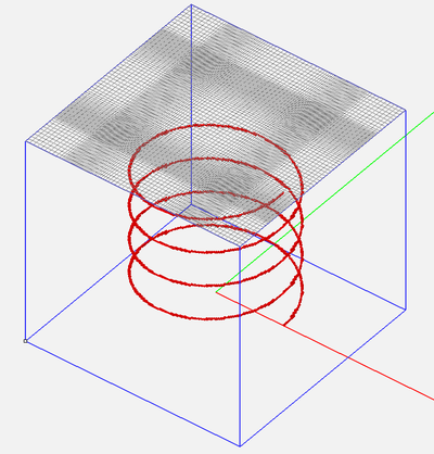
Figure 3. The geometry of a helix curve and its adaptive FDTD mesh.
FDTD Mesh Settings

EM.Cube's FDTD module discretizes objects using what is often referred to as the “staircase approximation”. In this mesh generation scheme, the structure is recreated using a large number of cubic cells carefully assembled in a way that approximates the shape of the original structure. By default, a carefully calculated, "Adaptive" mesh of your physical structure is generated in order to satisfy the following criteria:
- Optimize the number of mesh cells in each dimension. The product of the number of cells in each dimension determines the total mesh size. The larger the mesh size, the longer the simulation time, especially with the CPU version of the FDTD engine. Also, a very large mesh size requires more RAM, which may exceed your GPU memory capacity. Set the Minimum Mesh Density to a moderately low value to keep the mesh size manageable, but be careful not to set it too low (see the next item below).
- Ensure simulation accuracy by requiring an acceptable minimum number of cells per wavelength through each object and in the empty (free) space between them and the computational domain boundaries. An effective wavelength is defined for each material at the highest frequency of the project's specified spectrum. We recommend a Minimum Mesh Density of at least 15-20 cells/ wavelength. But for some resonant structures, 25 or even 30 cells per wavelength may be required to achieve acceptable accuracy. As you reduce the mesh density, the simulation accuracy decreases.
- Accurately represent and approximate the boundaries of edges or surfaces that are not grid-aligned by closely adhering to their geometric contours. This is controlled by the Minimum Grid Spacing Over Geometric Contours, which can be specified either as a fraction of the free space grid spacing or as an absolute length value in project units.
- Maximize the minimum grid spacing in any dimension inside the computational domain and thus maximize the simulation time step. The time step size is dictated by the CFL stability criterion and is driven by the smallest grid spacing in each dimension. The smaller the time step, the larger the number of time steps required for convergence. This is controlled using the Absolute Minimum Grid Spacing, which can be specified either as a fraction of the free space grid spacing or as an absolute value. It is critical to accurately represent and precisely maintain the object edge/surface boundaries in certain structures like resonant antennas and filters, as the phase of the reflected fields/waves is affected by the object boundary positions. When object boundaries are very close to each other, the mesh needs to represent them by two separate, but very closely spaced, grid lines. To control the minimum allowed grid spacing, use the Absolute Minimum Grid Spacing settings,
- Maintain a smooth grid with no abrupt jumps from low-density to high-density regions. This feature is enabled with the Create Gradual Grid Transitions check box (always checked by default).
Occasionally, you may prefer a more regular FDTD mesh with almost equal grid line spacing everywhere, but still with a frequency-dependent cell size. In that case, you can select the "Regular" option of the Mesh Type dropdown list in the FDTD Mesh Settings dialog. The regular FDTD mesh enforces only two of the above parameters: Minimum Mesh Density and Absolute Minimum Grid Spacing. Or you may opt for an absolutely "Uniform" mesh type, for which you need to specify the Cell Size along the X, Y, Z directions in project units.
Global vs. Local Control Of FDTD Mesh
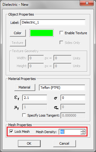
When EM.Cube generates an FDTD mesh, a large number of geometrical considerations are taken into account. These include the bounding box of each object and its corners, the ends of a line, the apex of a cone or pyramid, or the locations of lumped sources, field probes and sensors, vertices of plane wave or far field boxes, to name a few examples. These points are “locked” as fixed grid nodes in the FDTD mesh. EM.Cube determines these points internally to generate a mesh that best approximates the original structure. As you saw earlier, you can use the FDTD mesh settings to control the shape and resolution of the mesh, for example, around the curved portions of your structure, or on slanted lines or faces, etc. These settings are global and apply to all the objects making up your physical structure.
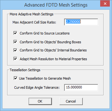
You can control the global mesh more selectively using the Advanced FDTD Mesh Settings Dialog. To open this dialog, click the Advanced button at the bottom of the FDTD Mesh Settings dialog. For example, you can control the quality of the gradual grid transitions by setting the value of Max Adjacent Cell Size Ratio. The default value of this parameter is 1.3, which maintains a smooth grid line spacing scheme with no more than 1:1.3 ratio for adjacent cells. By default, grid lines are enforced at all source and observable locations. You have the option to disable this feature and round up source locations to their closest grid lines. You may also uncheck the box labeled "Adapt mesh resolution to material properties". In that case, the same effective wavelength will be used to determine the mesh resolution inside all materials as well as the free-space regions.
Figure 1: FDTD Module's Advanced Mesh Settings dialog.
In certain cases, you may wish to exert some level of local mesh control. For example, you may want to increase the mesh density at a very particular area of your structure. Or you may want to increase or decrease the mesh resolution inside certain types of materials independent of their permittivity and permeability. EM.Cube provides two additional mechanisms for local control of the FDTD mesh: locking mesh of object groups and user defined fixed grid points. You can lock the mesh density of each material group. In this case, the areas inside and around the "Locked" material objects are meshed according to the locked mesh density, while the rest of the computational domain is meshed using the project's global mesh density. Locking mesh is done through the property dialog of each material group. At the bottom of the material property dialog, in the "Mesh Properties" section, there is a check box labeled Lock Mesh, which is unchecked by default. If you check this box, it enables the box labeled Mesh Density, which initially has a value equal to the project's global mesh density.
Figure 2: Locking the mesh density of a material group in its property dialog.
Adding Fixed Grid Points
Adding fixed grid points to an FDTD mesh increases its resolution locally. Each fixed grid point adds three grid lines along the three principal axes passing through that point. You can add as many fixed grid points as you desire and create dense meshes at certain regions. Fixed grid points appear as grey points in the project workspace. To insert a new fixed grid point, follow these steps:
- Open the Fixed Grid Points Dialog by selecting Menu > Simulate > Discretization > Fixed Grid Points... or by right clicking on the FDTD Mesh item of the Navigation Tree and selecting Fixed Grid Points Settings...
- Click the Add/Edit button to open the "Add Fixed Grid Point" dialog.
- Enter the (X, Y, Z) coordinates of the new fixed point in the coordinate boxes and click OK.
- To modify the coordinates of an existing fixed grid point, select it from the table and click the Add/Edit button.
- You can also remove a fix grid point from the FDTD mesh using the Delete button.
Figure 1: Adding a new fixed grid point in FDTD Module's Fixed Grid Points Settings dialog.
Figure 2: User defined fixed grid points in an FDTD mesh. (Left) Regular mesh, (Right) Adaptive mesh.
Excitation Sources
Before you can run an FDTD simulation, you have to define a source to excite your project’s physical structure. A physical source has a zero value at t = 0, but it rises from zero at t > 0 according to a specified waveform. EM.Cube's FDTD Module currently offers three types of temporal waveform:
- Sinusoidal
- Gaussian Pulse
- Modulated Gaussian Pulse
A sinusoidal waveform is single-tone and periodic. Its spectrum is concentrated around a single frequency, which is equal to your project's center frequency. A sinusoidal source does not have a finite energy and it does not decay as t → ∞. A Gaussian pulse decays exponentially as t → ∞, but it has a lowpass frequency spectrum which is concentrated around f = 0. A modulated Gaussian pulse decays exponentially as t → ∞, and it does have a bandpass frequency spectrum concentrated around your project's center frequency. For most practical problems, a modulated Gaussian pulse waveform provides an adequate performance. That is why this type of waveform is chosen by EM.Cube as your project's default waveform.
When an FDTD simulation starts, your project's source starts pumping energy into the FDTD computational domain at t > 0. Maxwell's equations are solved in all cells at every time step until the solution converges, or the maximum number of time steps is reached. If you use a Gaussian pulse or a modulated Gaussian pulse waveform to drive your FDTD source, after a certain number of time steps, the total energy of the computational domain drops to very negligible levels. At the point, you can consider your solution to have converged. If you drive your FDTD source by a sinusoidal waveform, the total energy of the computational domain will oscillate indefinitely, and you have to force the time loop to terminate after a certain number of time steps assuming a steady state have been reached.
EM.Cube's FDTD Module provides a number of sources or excitation schemes that have different applications. These source types will be described in the following sections. An Ideal Source is the simplest way of exciting a structure in EM.Cube's FDTD Module. It consists of an ideal voltage source connected between two consecutive nodes of your FDTD mesh. A Lumped Source is an ideal voltage source in series with a resistor. You have to place a lumped source on a line object that is parallel to one of the three principal axes, and you can assign a port to it to calculate the circuit characteristics of your structure. A Waveguide Source is placed across a rectangular waveguide. In other words, it requires a hollow box object that is aligned along one of the three principal axes and has one or two open ends. A waveguide source can excite a certain TEmn or TMmn modal profile of the host rectangular waveguide. A Distributed Source is defined on a finite-sized plane parallel to one of the three principal planes and with a prescribed field distribution profile on that plane. A Plane Wave Source is used to study the scattering characteristics of your structure and compute its radar cross section (RCS). A Gaussian Beam Source is similar to a plane wave source but with a focused energy profile in the transverse direction and a beam-diverging profile in the longitudinal direction.
Ideal Sources

An ideal source acts as a voltage source with a zero internal resistance that can be placed between any two adjacent mesh grid nodes anywhere in the computational domain. To create a new ideal source, follow these steps:
- Right click on the Ideal Sources item in the Sources section of the Navigation Tree and select Insert New Source... to open the Ideal Source Dialog.
- You can change the default name of the source as well as its color. The ideal source is displayed as a small orange arrow in the Project Workspace.
- By default, EM.Cube creates a +Z-directed ideal source located at the origin of coordinates (0, 0, 0). You can change the location of the source by setting new values for the X, Y and Z coordinates. When you use the spin buttons to increment or decrement the source coordinates, you can see the source moving in the project workspace. You can also change the Direction of the source from a dropdown list in the Source Location section of the dialog that contains ±X, ±Y and ±Z options.
- In the Source Properties section, you can specify the Source Amplitude in Volts and the Phase in Degrees.
Lumped Sources

A Lumped Source is the most commonly used way of exciting a structure in EM.Cube's FDTD Module. A lumped source acts as a voltage source in series with an internal resistance that is placed between two adjacent mesh grid nodes on a line object. The line object must be parallel to one of the three principal axes.
| |
In order to create a lumped source, you must have at least one line object in the project workspace. |
To create a new lumped source, follow these steps:
- Right click on the Lumped Sources item in the Sources section of the Navigation Tree and select Insert New Source... to open the Lumped Source Dialog.
- In the Source Location section of the dialog, you will find a list of all eligible line objects (i.e. lines that are parallel to one of the principal axes). Select the desired line object. The box labeled Direction shows the direction of the source with respect to the host line object. You have the option to select either the positive or negative direction for the source.
- In the box labeled Offset, enter the distance of the source from the start point of the line. A lumped source by default is placed at the center of the host line. In other words, the default offset value is equal to half the length of the host line object.
- In the Source Properties section, you can specify the source Amplitude in Volts, Phase in Degrees and internal Resistance in Ohms.
Waveguide Sources
Waveguide structures have many applications at microwave and millimeter wave frequencies. For example, a rectangular waveguide is used to feed a pyramidal horn antenna. A waveguide structure is usually excited using some type of strategically located probe mechanism. This can be modeled using a lumped source placed on a wire structure made up of line objects. Alternatively, use can use EM.Cube's Waveguide Sources, a special type of source that excites a prescribed modal field distribution in a rectangular waveguide structure. The scattering parameters are calculated from knowledge of incident and reflected fields at designated waveguide ports. Waveguide sources typically provide more accurate results for scattering parameters compared to lumped ports as they represent the actual dominant propagating modes at the transmission line ports.
EM.Cube provides special waveguide sources that can excite either the TEmn or TMmn modes of a rectangular waveguide which is oriented along one of the three principal axes. In other words, the plane of the waveguide source must be parallel to one of the principal (XY, YZ or ZX) coordinate planes.
| |
In order to create a waveguide source, you must have at least one "Hollow" Box object with no caps or only one end cap in your project. |
To create a new waveguide source, follow these steps:
- Right click on the Waveguide Sources item in the Sources section of the Navigation Tree and select Insert New Source... to open the Waveguide Source Dialog.
- In the Source Location section of the dialog, you will find a list of all the eligible box objects. These are all the hollow boxes in the project workspace whose longitudinal axis is parallel to one of the principal axes and have at least one unchecked Cap Ends box in their property dialog. Select the desired box object. The box labeled Direction shows the direction of the source with respect to the host box object. You have the option to select either the positive or negative direction for the source.
- In the box labeled Offset, enter the distance of the source plane from the base of the box object. A waveguide source by default is placed at the center of the host box. In other words, the default offset value is equal to half the length of the host box object.
- The default waveguide more to be excited is TE10. You can select TE or TM mode types with arbitrary "m" and "n" modal indices.
- In the Source Properties section, you can specify the source Amplitude in Volts, and the Phase in Degrees.
Figure 1: FDTD Module's Waveguide Source dialog.
Distributed Sources

Waveguide sources are a special case of distributed sources in EM.Cube's FDTD Module. A Distributed Source is defined in a rectangular plane of finite extents, parallel to one of the three principal coordinate planes. An impressed electric field component is assumed across the specified rectangular area, which pumps energy into the computational domain. The current version of EM.Cube provides three spatial field profiles for a distributed source:
- Uniform
- Sinusoidal
- Edge-Singular
The sinusoidal type has the functional form cos(py/w), and the edge-singular type has the functional form 1/v(1-(2y/w)^2), where y is the coordinate along the direction of field variation measured from the center of the rectangular area and w is its total width.
To create a new distributed source, follow these steps:
- Right click on the Distributed Sources item in the Sources section of the Navigation Tree and select Insert New Source... to open the Distributed Source Dialog.
- In the Excitation Plane section of the dialog, first you have to select the orientation of the source plane. The dropdown list labeled Direction gives three options: X, Y and Z, which create planes parallel to the YZ, ZX and XY principal planes, respectively. Depending on the choice of the plane orientation, another dropdown list labeled Field Dir gives four options for the direction of the source field component. For example, the default plane orientation is X (parallel to the YZ-Plane) and the available field directions are +Y, -Y, +Z and -Z. Next, you have to enter the coordinates of two opposite corners of the source plane: the lower left and upper right corners. You can type in values for the X, Y, Z coordinates or you can use the spin buttons to slide the default source planes in the Project Workspace.
- In the Source Properties section, you can select the Profile from three options: Uniform, Sinusoidal and Edge-Singular. You can also specify the source Amplitude in Volts, and Phase in Degrees and the source's internal Resistance in Ohms .
Figure 2: A distributed source placed between two horizontal rectangular strips.
Defining Ports
Ports are used to order and index sources for circuit parameter calculations like S/Y/Z parameters. That is why they are defined in the Observables section of Navigation Tree. In EM.Cube's FDTD Module, you can define ports at the location of Lumped Sources, Waveguide Sources and Distributed Sources. In other words, ideal sources or other types of sources cannot be used to define ports or calculate port characteristics.
Ports are defined in the Observables section of the Navigation Tree. Right click on the Port Definition item of the Navigation Tree and select Insert New Port Definition... from the contextual menu. The Port Definition Dialog opens up, showing the default port assignments. If you have N sources in your physical structure, then N default ports are defined, with one port assigned to each source according to their order on the Navigation Tree.
Figure: The Port Definition dialog.
You can define any number of ports equal to or less than the total number of sources in your project. The Port List of the dialog shows a list of all the ports in ascending order, with their associated sources and the port's characteristic impedance, which is 50O by default. You can delete any port by selecting it from the Port List and clicking the Delete button of the dialog. Keep in mind that after deleting a port, you will have a source in your project without any port assignment. Make sure that is what you intend. When you delete one or more ports in your project, their associated sources become free and "available" for either defining new ports or reassignment to the other ports. To define a new port, click the Add button of the Port Definition dialog to open the "Add Port" dialog. On the left side of this dialog, you will see a table containing all the available sources. Select one or more ports and use the right arrow (--->) button to move them to the table on the right side, labeled "Associated". These ports are now associated with the new port being defined. You can move sources from the "Associated" table back to the "Available" table on the left using the left arrow (<---) button of the dialog. You can associate more than one source with the same port. In that case, you will have coupled sources, collectively representing a coupled port.
Figure: Reassigning sources to ports and defining coupled ports.
| |
In order to obtain correct results, the port impedance must equal the characteristic impedance of the transmission line on which the port is established. This is not done automatically in EM.Cube. |
You can change the characteristic impedance of a port by selecting it from the Port List and clicking the Edit button of the dialog. This opens up the Edit Port dialog, where you can enter a new value in the box labeled Impedance.
Modeling Microstrip Line Ports
Using simple lumped sources, you can simulate a variety of transmission line structures in EM.Cube’s FDTD Module including filters, couplers or antenna feeds and you can calculate their scattering parameters. This approach may become less accurate at very high frequencies when the details of the feed structures become important and can no longer be modeled with highly localized lumped ports. In such cases, it is recommended to use “Distributed Sources”, which utilize accurate modal field distributions at the ports for calculation of the incident and reflected waves. This and next two sections explain how you can use simple lumped sources to model some popular transmission line feeds.
Microstrip ports can be modeled with lumped sources placed underneath the microstrip line stretching to the ground plane through the substrate. To build a microstrip port with a lumped source, follow these steps:
- First, draw the PEC microstrip using the Rectangle Strip Tool and end it at the desired port location.
- Then, draw the substrate box and make sure that its extends at least λg/8 beyond than the microstrip line (λg is the guide wavelength).
- If the microstrip's ground plane is the bottom of your simulation structure, set a PEC boundary for the bottom face of the computational domain. Otherwise, you do need to draw a PEC rectangle strip to represent a finite ground.
- Connect the center of the microstrip’s end to the ground plane with a PEC line using the Line Tool.
- Place a lumped source with 1V amplitude and zero phase on the line pointing towards the line.
- In the Port Definition Dialog, set the number of ports equal to one. Associate the lumped source with Port 1. Set the value of Port Impedance properly equal to the characteristic impedance of the microstrip feed line.
Figure 1: A microstrip line port on a substrate terminated from the bottom by a PEC boundary plane.
Modeling Coplanar Waveguide Ports
Using lumped sources, you can define coplanar waveguide (CPW) ports either with or without a bottom ground plane. In order to build a CPW port with a lumped source, follow these steps:
- First, draw the PEC center strip of the CPW with its two PEC coplanar ground planes, all using the Rectangle Strip Tool, and end them at the desired port location.
- Then, draw the substrate box and make sure that it is at least λg/8 longer than the CPW line.
- Connect the two end corners of the center strip to the two side ground planes with two PEC line objects using the Line Tool.
- Place a lumped source with 1V amplitude and zero phase on each line pointing towards the center strip.
- In the Port Definition Dialog, set the number of ports equal to one. Associate both of the lumped sources with Port 1. Set the value of the Port Impedance properly equal to the characteristic impedance of the CPW feed line.
EM.Cube sets the internal resistance of each of the two coupled lumped sources equal to twice the specified port (or line) impedance since the CPW port is a parallel connection of the two individual lumped sources. If you want to model a CPW with laterally infinite substrate and ground planes, make sure to set the domain offsets in the ±X and ±Y directions equal to zero. In the -Z direction, you need a nonzero offset to push the bottom CPML boundary down away outside the dielectric layer of finite thickness. Alternatively, you can terminate the bottom boundary by PEC and set its domain offset equal to zero to represent a CPW with a bottom PEC ground.
Figure 1: A coplanar waveguide (CPW) port on a dielectric substrate.
Modeling Coaxial Line Ports
Coaxial line is often used to feed various RF and microwave structures. In order to excite the dominant TEM mode of a coaxial line, it has to be fed symmetrically between its inner and outer conductors. Using lumped sources, you can define symmetrical coaxial line ports. To do so, follow these steps:
- First, use the Cylinder Tool to draw a solid PEC inner conductor and end it at the desired port location.
- Next, using the Cylinder Tool again, draw a hollow PEC outer conductor with the Cap Ends option unchecked, and end it at the desired port location.
- Then, draw the dielectric core of the coaxial cable using the Cylinder Tool under an active dielectric material group and make sure it is at least λg/8 longer than the inner and outer conductors. Note that you only need to draw a solid dielectric cylinder rather than a hollow, pipe-like one. According to FDTD Module's material hierarchy, the PEC core takes precedence over its enclosing dielectric cylinder.
- Using the Line Tool, connect the ends of the inner and outer conductors with four PEC line objects along the principal coordinate axes pointing from the inner conductor towards the outer conductor.
- Place a lumped source with 1V amplitude and zero phase on each line.
- In the Port Definition Dialog, set the number of ports equal to one. Associate all the four lumped sources with Port 1. Set the value of the Port Impedance properly equal to the characteristic impedance of the coaxial feed line.
Figure 1: A coaxial line port using four symmetric lumped sources.
Lumped Loads
In EM.Cube's FDTD Module you can define simple lumped elements such as resistors, inductors, capacitors as well as nonlinear diodes. Although lumped loads are not sources and do not excite a structure, their properties are similar to lumped sources. Lumped Loads are incorporated into the FDTD grid across two adjacent nodes in a similar manner to lumped sources. Likewise, lumped loads are defined on Line objects. In order to create a lumped load, you must have at least one line object in your project.
To create a new lumped load, follow these steps:
- Right click on the Lumped Loads item in the Sources section of the Navigation Tree and select Insert New Source... to open the Lumped Load Dialog.
- You can change the name of the lumped load as well as its color using the Color button of the dialog and selecting the desired color from the color palette.
- In the Lumped Element Location section of the dialog, you will find a list of all eligible line objects (i.e. lines that are parallel to one of the principal axes). Select the desired line object. The box labeled Direction shows the direction of the lumped load with respect to the host line object. Note that for a passive lumped load, the direction does not make any difference. But it matters for the case of a diode.
- In the box labeled Offset, enter the distance of the lumped element from the start point of the line. A lumped load by default is placed at the center of the host line. In other words, the default offset value is equal to half the length of the host line object.
- In the Lumped Element Properties Section, you can set the type of the load. In the dropdown list you have four options: Resistor, Inductor, Capacitor and Diode. The resistance is expressed in Ohms (O), inductance in Nano-Henry (nH) and capacitance in Pico-Farad (pF). In the case of a diode, you have to specify the Saturation Current in femto-Ampere (fA), the ambient Temperature in Degree Kelvin and also the diode's Ideality Factor, which is usually a number between 1 and 2.
Figure: FDTD Module's Lumped Load dialog with the load type set to resistor, inductor, capacitor and diode.
Sources & Loads For Antenna Arrays
If your project contains an array of line objects, you can also define an array of Lumped Sources to be placed on those lines. If you insert a new lumped source, all line array objects, if any, will be listed in the Lumped Source dialog as eligible objects for lumped source placement. A lumped source will be placed on each element of the array. All the lumped sources will have identical direction and offset. However, you can prescribe certain amplitude and/or phase distribution among the array elements. The available Weight Distributions include Uniform, Binomial, Chebyshev and Data File. In the last case, you need to set a value for maximum side lobe level (SLL) in dB. You can also define a Phase Progression in degrees along each of the three principal axes.
Figure 1: Defining lumped sources with a Chebyshev weight distribution on an array of line objects.
Just like lumped sources, you can place Lumped Loads on array of line objects. These loads can be resistors, capacitors, inductors or nonlinear diodes. If you insert a new lumped load, all line array objects, if any, will be listed in the Lumped Load dialog as eligible objects for lumped load placement. A lumped load will be placed on each element of the array. All the lumped load will have identical type, direction, offset and parameter values.
If the project workspace contains an array of hollow box objects to model a rectangular waveguide array, you can also define an array of Waveguide Sources to be placed across those waveguides. If you insert a new waveguide source, all hollow box array objects, if any, will be listed as eligible objects for waveguide source placement. A waveguide source will be placed on each element of the array. All the waveguide sources will have identical direction and offset. However, you can prescribe certain amplitude and/or phase distributions. The available Weight Functions include Uniform, Binomial, Chebyshev and Data File. In the last case, you need to set a value for maximum side lobe level (SLL) in dB. You can also define a Phase Progression in degrees along each of the three principal axes.
Plane Waves

In EM.Cube's FDTD Module, you can excite a structure with an arbitrary incident plane wave and compute its scattering pattern or bi-static radar cross section. A plane wave excitation is defined by its propagation vector indicating the direction of incidence and its polarization. EM.Cube's FDTD Module provides the following polarization options:
- TMz
- TEz
- Custom Linear
- LCPz
- RCPz
The direction of incidence is defined through the θ and φ angles of the unit propagation vector in the spherical coordinate system. The values of these angles are set in degrees in the boxes labeled Theta and Phi. The default incidence angles are θ = 180° and φ = 0° representing a normally incident plane wave propagating along the -Z direction with a +X-polarized E-vector. You select the polarization from the five radio buttons in the "Polarization" section of the dialog. In the TMz and TEz polarization cases, the magnetic and electric fields are parallel to the XY plane, respectively. The components of the unit propagation vector and normalized E- and H-field vectors are displayed in the dialog. This way of defining a plane wave source is more convenient when the structure is laid out along the XY plane and Z-axis such as layered and periodic structures. In the more general case of custom linear polarization, besides the incidence angles, you have to enter the components of the unit electric Field Vector. However, two requirements must be satisfied: ê . ê = 1 and ê × k = 0 . This can be enforced using the Validate button at the bottom of the dialog. If these conditions are not met, an error message is generated. The left-hand (LCP) and right-hand (RCP) circular polarization cases are restricted to normal incidences only (θ = 180°).
Since the FDTD technique requires a finite simulation domain, it also needs a finite plane wave incidence surface to calculate the excitation. When you create a plane wave source, a plane wave box is created as part of its definition. The time domain plane wave excitation is calculated on the surface of this box and injected into the computational domain. The plane wave box is displayed in the project workspace as a purple wireframe box enclosing the structure.
To create a new plane wave source, follow these steps:
- Right click on the Plane Waves item in the Sources section of the Navigation Tree and select Insert New Source... The Plane wave Dialog opens up.
- Initially, the radio button Size: Default is selected. With this option, the boundaries of the excitation box always have a distance of three cells from the bounding box of the geometry and cannot be changed. The radio button Size: Custom allows you to set the excitation box manually. The values for the coordinates of Corner 1 and Corner 2 can now be changed. Corner 1 is the front lower left corner and Corner 2 is the rear upper right corner of the box. The box has to be defined in grid coordinate system (GCS).
- In the Field Definition section of the dialog, you can enter the Amplitude of the incident electric field in V/m and its Phase in degrees. The default field Amplitude is 1 V/m with a zero Phase.
- The direction of the Plane Wave is determined by the incident Theta and Phi angles in degrees. You can also set the Polarization of the plane wave and choose from the five options described earlier.
A plane wave box placed around a PEC sphere object. The trident at the corner of the box shows the propagation vector as well as the E-field and H-field polarization vectors.
Focused Gaussian Beams

EM.Cube gives you an option to illuminate objects with a focused beam instead of a uniform plane wave. The focused beam is a Gaussian beam, which is a solution of the paraxial approximation to the Helmholtz equation. The fundamental Gaussian beam is rotationally-symmetric about its propagation axis, and its transverse field distribution follows a Gaussian function profile. The critical parameter is the beam radius w0; it is the point where the field drops by 1/e from its value at the center. The beam opens up into a cone along the propagation direction, with a cone angle of tan θ = λ0/(π.ω0) (λ0 is the free-space wavelength). The beam radius has to be at least λ0/π; otherwise, strong fields appear outside the excitation box.
The Gaussian beam box is displayed in the project workspace as a green wireframe box enclosing the structure. To define a new Gaussian Beam source, follow these steps:
- Right click on the Gaussian Beam item in the Sources section of the Navigation Tree and select Insert New Source... This opens up the Gaussian Beam Dialog.
- Similar to the plane wave, a default Excitation Box three cells away from the bounding box of the geometry is suggested, i.e. the radio button Size: Default is selected by default. The radio button Size: Custom allows you to set the excitation box manually by modifying the coordinates of Corner 1 (front lower left) and Corner 2 (back upper right) of the box in the grid coordinate system (GCS).
- In the Field Definition section of the dialog, you can enter the Amplitude of incident electric field in V/m. The default field Amplitude is 1 V/m. Note that you do not specify the phase of a Gaussian beam because the beam focus already contains the phase information.
- The direction of the Gaussian Beam is determined by the incident Theta and Phi angles in degrees. You can also set the Polarization of the Gaussian Beam and choose from the three options: TMz, TEz and User Defined.
- Unlike plane waves, a Gaussian beam is a localized field. Therefore, you need to specify the Beam Properties. This includes the coordinates of the beam's Focus, which is the beam's waist center in the world coordinate system as well as the beam's Radius in project units.
A Gaussian beam box placed around a horizontal PEC plate. The trident at the corner of the box shows the propagation vector as well as the E-field and H-field polarization vectors. The titled transparent green circle shows the footprint of Gaussian beam at its focal (waist) point.
Running FDTD Simulations
Strategy For An Accurate & Efficient FDTD Simulation
The FDTD method is one of the most versatile numerical techniques for solving electromagnetic modeling problems. Choosing the right settings and optimal values for certain numerical parameters will have a significant impact on both accuracy and computational efficiency of an FDTD simulation. Below are a number of steps that you should typically follow by order when planning your FDTD simulation:
- Identify material types and proper domain boundary conditions.
- Identify the source type and excitation mechanism.
- Define the project observables.
- Mesh the physical structure and examine the quality of the generated mesh and it geometric fidelity.
- Determine the proper temporal waveform.
- Select the simulation mode and run the FDTD engine.
For certain problems, more than one combination or choice of settings and parameters may still give acceptable results. In most cases, EM.Cube tries to make these choices convenient for you by suggesting default settings or default parameter values. For example, EM.Cube by default generated am "adaptive" type mesh with a default density of 20 cells per effective wavelength. The default computational domain features CPML walls placed a quarter free-space wavelength away from the large bounding box of the entire physical structure. A modulated Gaussian waveform with certain optimal parameters is used to drive the project's excitation source by default. You can change most of these settings arbitrarily. For example, you can set up your own computational domain with different types of boundary conditions, customize the FDTD mesh by modifying a large number of mesh settings and use other types of excitation waveforms.
FDTD Observable Types
In EM.Cube, project observables are the simulation data that are generated by the simulation engine at the end of each simulation run. EM.Cube's FDTD simulation engine calculates all the six electric and magnetic field components (Ex, Ey, Ez, Hx, Hy and Hz) at every mesh grid node at all time steps from t = 0 until the end of the time loop. However, in order to save memory space, the engine has to destroy the temporal field data from each time step to the next and reuse the memory. Storage, manipulation and visualization of 3D data can become overwhelming for complex structures and larger computational domains. Furthermore, calculation of some field characteristics such as radiation patterns or radar cross section (RCS) can be sizable, time-consuming, post-processing tasks. That is why EM.Cube asks you to define project observables to instruct why types of simulation data you seek in each simulation effort.
EM.Cube's FDTD Modules currently offers the following types of observable:
- Field Probes
- Field Sensors
- Domain Energy
- Far Field - Radiation Patterns
- Far Field - RCS
- Huygens Surface Data
- Port Characteristics (S/Y/Z Parameters and VSWR)
- Reflection and Transmission Coefficients
Field probes monitor the field components at a certain point in the computational domain. They record the time-domain field data during the entire time loop and compute their frequency spectrum using a discrete Fourier transform. Field sensors are primarily intended for observation of near field maps on a certain cross section of the computational domain. The field sensor planes are parallel to one of the three principal XY, YZ or ZX planes. When you run a frequency sweep or parametric sweep, multiple maps are generated for each sample of your sweep variable, and you can animate these maps. You can also animate the evolution of the near fields in the time domain over the course of the simulated time loop. EM.Cube can also keep track of the electric, magnetic and total energy of the computational domain as functions of the time step.
Using asymptotic near-to-far-field transformations, EM.Cube calculates the far fields of your physical structure in the standard spherical coordinate system. The radiation patterns are indeed the spherical electric field components Eθ and Eφ expressed as functions of the observation angles θ and φ over a unit sphere. The far field data are calculated in the frequency domain at a specified frequency, which is equal to your project's center frequency by default. When your excitation source is a plane wave or a Gaussian beam, the far field data actually represent the scattering behavior of your "target". In the case of a plane wave source, the FDTD simulation engine can also compute the radar cross section of you target. If your structure is periodic, then the reflection and transmission coefficients of the periodic surface are also calculated over the entire bandwidth of your project.
You can define ports for lumped sources, waveguide sources and distributed sources. In that case, the FDTD simulation engine calculates the scattering (S) parameters of your multiport network over the entire bandwidth specified in your project. From the scattering matrix, EM.Cube determines the impedance and admittance matrices of your network over the operational bandwidth. You can plot the S/Y/Z parameters in EM.Grid. If your project has more than one port, the FDTD time loop will be run as many times as the number of ports, N. In each time loop run j (j = 1, 2, ..., N), the source(s) associated with the jth port is (are) excited with a unit amplitude and all the other sources are turned off. In this run, all the Sij parameters (i = 1, 2, ..., N) are calculated. At the end of the Nth run, the entire S matrix is completed.
The FDTD Simulation Engine Settings

An FDTD simulation involves a number of numerical parameters that can be accessed and modified from the FDTD Engine Settings Dialog. To open this dialog, select Menu > Simulate > Simulation Engine Settings... or open the Run Dialog, and click the Settings button next to the engine dropdown list.
In the " Convergence " section of the dialog, you can set the Termination Criterion for the FDTD time loop. The time loop must stop after a certain point in time. If you use a decaying waveform like a Gaussian pulse or a Modulated Gaussian pulse, after certain number of time steps, the total energy of the computational domain drops to very negligible values, and continuing the time loop thereafter would not generate any new information about your physical structure. By contrast, a sinusoidal waveform will keep pumping energy into the computational domain forever, and you have to force the simulation engine to exit the time loop. EM.Cube's FDTD Module provides two mechanism to terminated the time loop. In the first approach, an energy-like quantity defined as Un = Σ [ ε0|Ei,n|2 + μ0|Hi,n|2 ].ΔVi is calculated and recorded at a large random set of points in the computational domain. Here i is the space index and n is the time index. The quantity Un has a zero value at t = 0 (i.e. n = 0), and its value starts to build up over time. With a Gaussian or Modulated Gaussian pulse waveform, Un reach a maximum value Umax at some time step and starts to decline thereafter. The ratio 10.log( Un/ Umax) expressed in dB is used as the convergence criterion. When its value drops below certain Power Threshold, the time loop is exited. The default value of Power Threshold is -30dB, meaning that the FDTD engine will exit the time loop if the quantity Un drops to 1/1000 of its maximum value ever. The second termination criterion is simply reaching a Maximum Number of Time Steps , whose default value set to 10,000. A third option, which is EM.Cube's default setting (labeled "Both"), terminates the simulation as soon as either of the first two criteria is met first.
| |
Keep in mind that for highly resonant structures, you may have to increase the maximum number of time steps to very large values above 20,000. |
The "Acceleration" section of the FDTD Simulation Engine Settings dialog give three options for the FDTD kernel:
- Serial CPU Solver
- Multi-Core CPU Solver
- GPU Solver
The serial CPU solver is EM.Cube's basic FDTD kernel that run the time marching loop on a single central processing unit (CPU) of your computer. The default option is the multi-core CPU solver. This is a highly parallelized version of the FDTD kernel based on the Open-MP framework. It takes full advantage of a multi-core, multi-CPU architecture, if your computer does have one. The GPU solver is a hardware-accelerated FDTD kernel optimized for CUDA-enabled graphical processing unit (GPU) cards. If your computer has a fast NVIDIA GPU card with enough onboard RAM, the GPU kernel can speed up your FDTD simulations up to 50 times or more over the single CPU solver.
For structures excited with a plane wave source, there are two standard FDTD formulations: Scattered Field (SF) formulation and Total Field - Scattered Field (TF-SF) formulation. EM.Cube's FDTD module offers both formulations. The TF-SF solver is the default choice and is typically much faster than the SF solver for most problems. In two cases, when the structure has periodic boundary conditions or infinite CPML boundary conditions (zero domain offsets), only the SF solver is available. The other sections of the FDTD Simulation Engine Settings dialog will be described next in the context of Waveforms and Discrete Fourier Transforms.
Running A Wideband FDTD Simulation
Once you build your physical structure in the project workspace and define an excitation source, you are ready to run an FDTD simulation. The simulation engine will run even if you have not defined any observables. Obviously, no simulation data will be generated in that case. EM.Cube's FDTD Module currently offers several different simulation modes as follows:
- Analysis
- Frequency Sweep
- Parametric Sweep
- Angular Sweep
- R/T Macromodel
- Dispersion Sweep
- Huygens Sweep
- Optimization
- HDMR
Analysis is the simplest and most straightforward simulation mode of the FDTD Module. It runs the FDTD time marching loop once. At the end of the simulation, the time-domain field data are transformed into the frequency domain using a discrete Fourier transform (DFT). As a result, you can generate wideband frequency data from a single time-domain simulation run. The other simulation modes will be explained later in this manual.
To open the Simulation Run Dialog, click the Run ![]() button of the Simulate Toolbar or select Menu > Simulate > Run... from the menu bar or use the keyboard shortcut Ctrl+R.
button of the Simulate Toolbar or select Menu > Simulate > Run... from the menu bar or use the keyboard shortcut Ctrl+R.
Figure 1: EM.Cube's FDTD Simulation dialog.
To start the FDTD simulation, click the Run button at the bottom of this dialog. Once the simulation starts, the "Output Window" pops up and reports messages during the different stages of the FDTD simulation. During the FDTD time marching loop, after every 10th time step, the output window updates the values of the time step, elapsed time, the engine performance in Mega-cells per seconds, and the value of the convergence ratio Un/Umax in dB. An EM.Cube FDTD simulation is terminated when the ratio Un/Umax falls below the specified power threshold or when the maximum number of time steps is reached. You can, however, terminate the FDTD engine earlier by clicking the Abort Simulation button.
Figure 2: FDTD Module's output window.
Waveforms & Discrete Fourier Transforms
The accuracy of the FDTD simulation results depends on the right choice of temporal waveform. The excitation waveform is the temporal source function that sets the initial conditions at t = 0 and provides an excitation signal afterwards. EM.Cube currently offers three choices:
- Sinusoidal
- Gaussian Pulse
- Modulated Gaussian Pulse
EM.Cube's default waveform choice is a modulated Gaussian pulse. At the end of an FDTD simulation, the time domain field data are transformed into the frequency domain at your specified frequency. This is usually the same as the center frequency of your project. Different waveforms have different spectral behaviors. It is critical that you understand the time-domain-to-frequency-domain transformations in order to correctly interpret some simulation data.
From the "Excitation Waveform" section of the FDTD Simulation Engine Settings dialog, you can override EM.Cube's default waveform and customize your own. The sinusoidal waveform has a frequency f0 equal to the project's center frequency and does not have any parameter that you can modify. The delay in this case is set to t0 = 1/(4f0) so that the waveform vanishes at t = 0:
where sinc(x) = sin(πx) / (πx), and T is the length of the temporal window from t = 0 to the exit time t = NΔt, and Δt is the time step of the time marching loop.
For Gaussian and modulated Gaussian waveforms you can set the pulse width and time delay. The pulse width should be chosen such that the Fourier transform of your selected waveform encompasses your project bandwidth. Rather than setting an arbitrary pulse width, EM.Cube lets you set a parameter called Spectral Truncation Level or delta (δ), which is the normalized truncation threshold for the spectral content of the excitation pulse. This is explained as follows. Recall that the Fourier transform of a Gaussian pulse is also a Gaussian pulse. The Fourier transform of a modulated Gaussian pulse consists of two Gaussian pulses located at the two opposite sides of f = 0 (DC) shifted by the modulation frequency f0:
Since a Gaussian pulse waveform has considerable DC content, it must be used to model lowpass structures. In that case, the center frequency and bandwidth of the project must be set such that Δf = 2f0 and hence, fmin = f0 - Δf/2 = 0, and fmax = f0 + Δf/2 = 2f0. The width t of the temporal Gaussian pulse is then determined such that at fmax the spectral Gaussian pulse drops to the d-level from its maximum value of 1. With a bandwidth of Δf, the pulse width must satisfy the following equation:
- [math] \exp[-(\pi f_{\delta} \tau)^2] = \exp[-(\pi \Delta f \tau)^2] = \delta \quad \Rightarrow \quad \tau = \frac{\sqrt{-\ln\delta}}{\pi f_{max}} [/math]
When you set δ = 0.1 (the default value), it means that the Fourier transform of your excitation waveform drops to 10% of its peak at the upper edge of your specified frequency range. For a Modulated Gaussian pulse waveform with a bandwidth of Δf, the pulse width must satisfy the following equation:
- [math] \exp[ -[\pi(f_{\delta} - f_0)\tau] ^2 ] = \exp \left[ -\left(\pi \frac{\Delta f}{2} \tau\right)^2 \right] = \delta \quad \Rightarrow \quad \tau = \frac{2\sqrt{-\ln \delta}}{\pi \Delta f} [/math]
For the default value of δ = 0.1, you get the standard relation: τ = 0.966 / BW, which is typically used for modulated Gaussian waveforms. The source waveform requires a time delay t0 so that its value drops to almost zero at t = 0. The time delay is expressed in terms of a multiple of the pulse width: t0 / tau, and its default value is 4.5.
Keep in mind that FDTD is a time domain algorithm. At the end of an FDTD simulation, a Discrete Fourier Transform (DFT) is performed on the time domain data to calculate frequency domain characteristics such as near fields, far field radiation patterns, RCS, S/Y/Z parameters, etc.:
- [math] \tilde{F}(f) = \int_{-\infty}^{\infty} f(t) e^{-j2\pi f t} \, dt \quad \approx \quad \Delta t \sum_{n=0}^N f(n\Delta t) e^{-j2 \pi n f \Delta t} [/math]
Of FDTD Module's observables, the near fields, far fields and all of their associated parameters like directivity, RCS, etc., are calculated at a certain frequency that is specified as part of the definition of the observable. On the other hand, port characteristics like S/Y/Z parameters, VSWR and periodic characteristics like reflection and transmission coefficients, are calculated over the entire specified bandwidth of your project. In other words, you get a wideband frequency response at the end of a single time domain FDTD simulation run. The number of frequency point data over this bandwidth is equal to the number of DFT samples that are generated during the time marching loop. This number is set to 200 by default. In other words, 200 frequency data are generated at the end of an FDTD simulation. You can change this number through the box labeled No. DFT Samples in the "Discrete Fourier Transform" section of the FDTD Simulation Engine Settings dialog.
It can be seen that the discrete Fourier transform multiplies the samples of time-domain field quantities by the time step Δt. This means that the resulting Fourier transforms of electric and magnetic field components now have units of V/m/Hz or A/m/Hz, respectively. Moreover, the Fourier transforms of the three waveform types have different spectral values at the observation frequency f0. This makes it difficult to compare the FDTD simulation results with the results from EM.Cube's other computational modules. For example, in the Planar, MoM3D and Physical Optics Modules, a plane wave source typically has a complex-valued functional form of exp(-jk0k.r), which has a unit magnitude. In FDTD Module, the time domain plane wave source has a functional dependence of the following form:
where f(t) is the temporal waveform, t0 is the time delay, l0 is a spatial shift, and c is the speed of light in the free space. The Fourier transform of the above temporal function evaluated at f = f0 has an amplitude different than 1. For this purpose, EM.Cube's FDTD Module normalizes the temporal waveform by the magnitude of its Fourier transform at the observation frequency f0. As a result, a temporal plane source with any of the three waveform types will always create spectral incident source with |Einc(r, f0)| = 1. The temporal waveform normalization factors for the three waveform types are given below:
Probing Fields in Time and Frequency Domains
By computing the time domain fields at a certain location, you can examine the transient response of a system at that location. This is also very useful for monitoring the convergence of FDTD time marching loop. EM.Cube's field probes allow you to save the temporal values of a field component at a specified point in the computational domain during the entire time marching loop. You can plot the time domain field components as a function of the time step index. You can also plot the spectral contents of those field components, i.e. their Fourier transform, over the project's specified frequency bandwidth. To define a new field probe, follow these steps:
- Right click on the Field Probe item in the Observables section of the Navigation Tree and select Insert New Observable...
- You can change the default name of the probe as well as its color. The field probe is displayed as a small green arrow in the Project Workspace.
- By default EM.Cube creates a field probe located at the origin of coordinates (0,0,0). You can move the probe to any location by changing its X, Y and Z coordinates.
- In the Probe Location section of the dialog, you can also set the Direction of the probe from a dropdown list that contains ±X, ±Y and ±Z options. The default direction is +Z.
Figure 1: FDTD Module's Field Probe dialog and an X-directed probe placed above a PEC plate illuminated by a normally incident plane wave.
At the end of an FDTD simulation, the electric and magnetic field components along the specified probe direction are saved at the probe's location. Both the time domain fields from t = 0 to the last time step and their frequency domain spectrum are recorded. You can plot these data in EM.Grid, which can be accessed from EM.Cube's Data Manager. To open data manager, click the Data Manager ![]() button of the Simulate Toolbar, or select Simulate > Data Manager from the menu bar, or right click on the Data Manager item of the Navigation Tree and select Open Data Manager... from the contextual menu, or use the keyboard shortcut Ctrl+D. In the Data manager Dialog, you see a list of all the data files available for plotting. These include the time-domain and frequency-domain probe data files with .DAT and .CPX file extensions, respectively. Select any data file by clicking and highlighting its row in the table and then click the Plot button to plot the graph. The time-domain field probe is plotted on a Cartesian graph showing the selected field component as a function of time step. The frequency-domain probe contains two Cartesian graphs: amplitude and phase of the selected field component over the project's frequency range.
button of the Simulate Toolbar, or select Simulate > Data Manager from the menu bar, or right click on the Data Manager item of the Navigation Tree and select Open Data Manager... from the contextual menu, or use the keyboard shortcut Ctrl+D. In the Data manager Dialog, you see a list of all the data files available for plotting. These include the time-domain and frequency-domain probe data files with .DAT and .CPX file extensions, respectively. Select any data file by clicking and highlighting its row in the table and then click the Plot button to plot the graph. The time-domain field probe is plotted on a Cartesian graph showing the selected field component as a function of time step. The frequency-domain probe contains two Cartesian graphs: amplitude and phase of the selected field component over the project's frequency range.
Figure 2: The time domain and frequency domain field components plotted vs. time and frequency, respectively.
Frequency-Domain Near Field Visualization

In EM.Cube you can visualize the near fields at a specific frequency in a specific plane of the computational domain. At the end of an FDTD simulation, all the time domain electric and magnetic field values are available at all mesh nodes. These temporal quantities are transformed into the frequency domain using discrete Fourier transforms to calculate the electric and magnetic fields on a specified sensor plane. To define a new Field Sensor, follow these steps:
- Right click on the Field Sensors item in the Observables section of the Navigation Tree and select Insert New Observable...
- The Label box allows you to change the sensor’s name.
- Set the Direction of the field sensor. This is specified by the normal vector of the sensor plane. The available options are X, Y and Z, with the last being the default option.
- By default EM.Cube creates a field sensor plane passing through the origin of coordinates (0,0,0) and coinciding with the XY plane. Note that the sensor plane extends across the entire computational domain. You can change the location of the sensor plane to any point by typing in new values for the X, Y and Z coordinates. Keep in mind that you can move a sensor plane only along the specified direction of the sensor. Therefore, only one coordinate can effectively be changed. As you increment or decrement this coordinate, you can observe the sensor plane moving along that direction in the project workspace.
- The frequency at which the field is evaluated has to be specified in the box labeled Near Field Frequency in the project's frequency unit. By default, this is equal to the project's center frequency.
After closing the Field Sensor Dialog, the a new field sensor item immediately appears under the Observables section in the Navigation Tree and can be right clicked for additional editing. Once an FDTD simulation is finished, a total of 14 plots are added to every Field Sensor node in the Navigation Tree. These include the magnitude and phase of all three components of E and H fields and the total electric and magnetic field values at the specified frequency. Click on any of these items and a color-coded intensity plot of it is visualized in the project workspace. A legend box appears in the upper right corner of the field plot, which can be dragged around using the left mouse button. The values of the magnitude plots are normalized between 0 and 1. The legend box contains the minimum field value corresponding to 0 of the color map, maximum field value corresponding to 1 of the color map, and the unit of the field quantity, which is V/m for E-field and A/m for H-field. The values of phase plots are always shown in Radians between -p and p. To display the fields properly, the structure is cut through the field sensor plane, and only part of it is shown. If the structure still blocks your view, you can simply hide or freeze it. You can change the view of the field plot with the available view operations such as rotating, panning, zooming, etc.
Figure 2: A horizontal field sensor plane showing the total electric and magnetic fields above a PEC plate illuminated by a normally incident plane wave.
You can plot frequency domain fields in EM.Grid on 2D Cartesian graphs. Using field probes, you can plot any frequency domain field component as a function of frequency over the specified bandwidth at any point within the computational domain. Using field sensors, you can plot the total frequency domain fields as a function of position (spatial coordinates) across the computational domain. Every field sensor has a crosshair made up of two perpendicular lines parallel to the boundaries of the sensor plane. When you define a field sensor for the first time, the crosshair passes through the origin of coordinates. You can change the location of the crosshair on the sensor plane using the other two coordinate boxes besides the one that moves the location of the sensor plane. At the end of an FDTD simulation, in addition to the 3D near field maps, EM.Cube also generates 2D Cartesian graphs of the total electric and magnetic fields along the two perpendicular crosshair lines. A total of four Cartesian data files are generated, two for total E-field and two for total H-field along the two lines. You can plot these data in EM.Grid, which can be accessed from EM.Cube's Data Manager. To open data manager, click the Data Manager ![]() button of the Simulate Toolbar, or select Simulate > Data Manager from the menu bar, or right click on the Data Manager item of the Navigation Tree and select Open Data Manager... from the contextual menu, or use the keyboard shortcut Ctrl+D. In the Data Manager dialog, you see a list of all the data files available for plotting including the frequency-domain sensor data files with a .DAT file extension. Select any data file by clicking and highlighting its row in the table and then click the Plot button to plot the graph. Frequency domain field sensor graphs show the total field as a function of cell index along one of the principal axes. If the FDTD mesh is uniform in that direction, the position is found by multiplying the cell index by the cell dimension and offsetting with respect to lower-front-left corner of the computational domain.
button of the Simulate Toolbar, or select Simulate > Data Manager from the menu bar, or right click on the Data Manager item of the Navigation Tree and select Open Data Manager... from the contextual menu, or use the keyboard shortcut Ctrl+D. In the Data Manager dialog, you see a list of all the data files available for plotting including the frequency-domain sensor data files with a .DAT file extension. Select any data file by clicking and highlighting its row in the table and then click the Plot button to plot the graph. Frequency domain field sensor graphs show the total field as a function of cell index along one of the principal axes. If the FDTD mesh is uniform in that direction, the position is found by multiplying the cell index by the cell dimension and offsetting with respect to lower-front-left corner of the computational domain.
Figure 3: Cartesian graph of total magnetic field vs. Y-index along the crosshair in the field senor plane.
Visualizing Field Evolution in Time Domain
In the course of the FDTD time marching process, a tremendous amount of data are generated that include all the six E/H field components at every Yee cell and at every time step. The temporal field values at a sensor plane are of particular interest. Such plots show the evolution of the fields as a function of time starting from time t = 0, when all the fields are zero everywhere in the computational domain. EM.Cube can record snapshots of the field sensor data as the time loop marches forward. When you define a field sensor for the first time, by default it displays the frequency domain near field data. In order to record and save the time domain data, you have to open the field sensor's property dialog by right clicking on the field sensor's name in the Navigation Tree and selecting Properties...from the contextual menu. In the section titled Sensor Domain, select the radio button labeled Time Domain. Also, in the section titled "Field Display - Multiple Plots", select one of the two radio buttons labeled E-Field or H-Field. By default, the time domain field data are saved every 100 time steps. To change this setting, right click on the Field Sensors item in the Navigation Tree and select Time Domain Settings... from the contextual menu. In the Time Domain Settings Dialog, change the value of the box labeled Sampling Interval (in time steps).
Time domain animation is available only for FDTD simulations of "Analysis" type. It cannot be used in conjunction with sweep simulations. Once the FDTD Analysis is finished, you can click any of the field plots and visualize it in the main window or you can animate them by right clicking on the field sensor's name in the Navigation Tree and selecting Animation from the contextual menu. You can change the animation settings from the Animation Controls Dialog. Note that the animation loop repeats itself indefinitely until you close the Animation Controls dialog or hit the keyboard’s Esc Key.
Figure 1: (Left) Changing a field sensor's domain to generate time-domain field data for animation, and (Right) FDTD Module's Time Domain Settings dialog.
Figure 2: Animation of E-field plots in time domain.
Scattering Parameters and Port Characteristics
If your physical structure is excited by a Lumped Source or a Waveguide Source or a Distributed Source, and one or more ports have been defined, the FDTD engine calculates the scattering (S) parameters, impedance (Z) parameters and admittance (Y) parameters of the selected ports. The S parameters are calculated based on the port impedances specified in the project's "Port Definition". If more than one port has been defined in the project, the FDTD engine runs an internal port sweep. Each port is excited separately with all the other ports turned off. When the jth port is excited, all the Sij parameters are calculated together based on the following definition:
- [math] S_{ij} = \sqrt{\frac{Re(Z_i)}{Re(Z_j)}} \cdot \frac{V_j - Z_j^*I_j}{V_i+Z_i I_i} [/math]
where Vi is the voltage across Port i, Ii is the current flowing into Port i and Zi is the characteristic impedance of Port i. The sweep loop then moves to the next port until all ports have been excited. After the FDTD simulation is finished, the S parameters are written into output ASCII data files. Since these data are complex, they are stored as .CPX files. Every file begins with a header starting with "#". Besides the scattering parameters, the admittance (Y) and impedance (Z) parameters are also calculated and saved in complex data files with .CPX file extensions. The following relationships are used:
- [math]\mathbf{ [Z] = [\sqrt{Z_0}] \cdot ([U]+[S]) \cdot ([U]-[S])^{-1} \cdot [\sqrt{Z_0}] }[/math]
- [math] \mathbf{ [Y] = [Z]^{-1} } [/math]
where [math]\mathbf{[U]}[/math] is the identity matrix of order N, and [math]\mathbf{\sqrt{Z_0}}[/math] is a diagonal matrix whose diagonal elements are the square roots of port characteristic impedances. The voltage standing wave ratio (VSWR) of the structure at the first port is also computed and saved to a real data .DAT file. The following definition is used:
- [math] \text{VSWR} = \frac{|V_{max}|}{|V_{min}|} = \frac{1+|S_{11}|}{1-|S_{11}|} [/math]
You can plot the port characteristics from the Navigation Tree. Right click on the Port Definition item in the Observables section of the Navigation Tree and select one of the items: Plot S Parameters, Plot Y Parameters, Plot Z Parameters, or Plot VSWR. In the first three cases, another sub-menu gives a list of individual port parameters. Keep in mind that in multi-port structures, each individual port parameter has its own graph. You can also see a list of all the port characteristics data files in EM.Cube's data manager. To open data manager, click the Data Manager ![]() button of the Simulate Toolbar or select Simulate > Data Manager from the menu bar or right click on the Data Manager item of the Navigation Tree and select Open Data Manager... from the contextual menu or use the keyboard shortcut Ctrl+D. Select any data file by clicking and highlighting its row in the table and then click the Plot button to plot the graph in EM.Grid. By default, the S parameters are plotted as dual magnitude-phase graphs, while the Y and Z parameters are plotted as dual real-imaginary part graphs. The VSWR data are plotted on a Cartesian graph. You change the format of complex data plots. In general complex data can be plotted in three forms:
button of the Simulate Toolbar or select Simulate > Data Manager from the menu bar or right click on the Data Manager item of the Navigation Tree and select Open Data Manager... from the contextual menu or use the keyboard shortcut Ctrl+D. Select any data file by clicking and highlighting its row in the table and then click the Plot button to plot the graph in EM.Grid. By default, the S parameters are plotted as dual magnitude-phase graphs, while the Y and Z parameters are plotted as dual real-imaginary part graphs. The VSWR data are plotted on a Cartesian graph. You change the format of complex data plots. In general complex data can be plotted in three forms:
- Magnitude and Phase
- Real and Imaginary Parts
- Smith Chart
In particular, it may be useful to plot the Sii parameters on a Smith chart. To change the format of a data plot, select it and click the Edit button of Data Manager and select one of the available graph type options.
Figure 1: EM.Cube's data manager showing a list of complex data files available for plotting in EM.Grid.
Figure 2: Plot of S21 of a filter in EM.Grid.
Far Field Calculations in FDTD
For radiating structures or scatterers, the far field quantities are of primary interest. EM.Cube's FDTD Module can calculate the far field radiation patterns of an antenna or the radar cross section (RCS) of a target. In general, by far fields we mean the electric fields evaluated in the far zone of a physical structure, which satisfies the following condition:
- [math]r \lt\lt \frac{2D^2}{\lambda_0}[/math]
where r is the distance between the observation and source points, λ0 is the free space wavelength and D is the largest dimension of the radiating structure. In EM.Cube, the far-zone electric fields Eff(θ, φ) are functions of the spherical observation angles only and are defined as
- [math] \begin{align} & \mathbf{E(r) = E} (r,\theta,\phi) = \frac{e^{-jk_0 r}}{r} \mathbf{E^{ff}}(\theta,\phi) \\ & \mathbf{H(r) = H} (r,\theta,\phi) = \frac{1}{\eta_0} \mathbf{ \hat{r} \times E^{ff}(r) } \end{align} \quad k_0 r \gt\gt 1 [/math]
where k0 = 2π/λ0 and η0 = 120π Ω is the intrinsic impedance of the free space.
In the FDTD method, the far fields are calculated using a near-field-to-far-field transformation of the field quantities on a given closed surface. EM.Cube uses rectangular boxes to define these closed surfaces. You can use EM.Cube's default radiation box or define your own. The far-zone electric field can be written as:
where J and M are the equivalent electric and magnetic surface currents on the surface of the enclosing box. GA,ff is the asymptotic form of the dyadic Green's function associated with the magnetic vector potential A and GEM,ff is the asymptotic form of the dyadic Green's function of the electric field due to a magnetic current. In most FDTD problems, the background medium of your physical structure is the free space and these functions reduce to the much simpler and familiar free-space Green's function: exp(-jk0r)/(4πr). In that case, one can define a pair of electric and magnetic radiation integrals:
- [math] \begin{align} & \mathbf{N(r)} = \iint_S \mathbf{J(r')} e^{ -jk_0 \mathbf{\hat{r} \cdot r'} } \, ds' \\ & \mathbf{L(r)} = \iint_S \mathbf{M(r')} e^{ -jk_0 \mathbf{\hat{r} \cdot r'} } \, ds' \\ \end{align} [/math]
where
- [math] \mathbf{\hat{r}} = \sin\theta \cos\phi \mathbf{\hat{x}} + \sin\theta \sin\phi \mathbf{\hat{y}} + \cos\theta \mathbf{\hat{z}} [/math]
In that case, the θ and φ components of the far fields can be computed from the following relationships:
- [math] \begin{align} & E_{\theta}^{ff}(\theta, \phi) = -\frac{jk_0}{4\pi} (L_{\phi} + \eta_0 N_{\theta}) \\ & E_{\phi}^{ff}(\theta, \phi) = \frac{jk_0}{4\pi} (L_{\theta} + \eta_0 N_{\phi}) \end{align} [/math]
where the θ and φ components of the radiation integrals are given by:
- [math] \begin{align} & N_{\theta}(\theta,\phi) = \iint_S [J_x\cos\theta\cos\phi + J_y\cos\theta\sin\phi - J_z\sin\theta] e^{ jk_0 \mathbf{\hat{r} \cdot r'} } \, ds' \\ & N_{\phi}(\theta,\phi) = \iint_S [-J_x \sin\phi + J_y\cos\phi] e^{ jk_0 \mathbf{\hat{r} \cdot r'} } \, ds' \end{align} [/math]
- [math] \begin{align} & L_{\theta}(\theta,\phi) = \iint_S [M_x\cos\theta\cos\phi + M_y\cos\theta\sin\phi - M_z\sin\theta] e^{ jk_0 \mathbf{\hat{r} \cdot r'} } \, ds' \\ & L_{\phi}(\theta,\phi) = \iint_S [-M_x \sin\phi + M_y\cos\phi] e^{ jk_0 \mathbf{\hat{r} \cdot r'} } \, ds' \end{align} [/math]
Normally, the radiation box should enclose the entire FDTD structure. In this case, the calculated radiation pattern corresponds to the entire radiating structure. The radiation box may contain only parts of a structure, which results in partial radiation patterns. In calculating the far field quantities, using Poynting's theorem, one can define the radiated power density as:
- [math] \mathbf{W} = \frac{1}{2} \text{Re}(\mathbf{E \times H^*}) = \frac{\mathbf{\hat{k}}}{2\eta_0} |\mathbf{E}(r,\theta,\phi)|^2 \, |_{r \to \infty} [/math]
To eliminate the dependency on r, a normalized quantity called "Radiation Intensity" in the following way:
- [math] S(\theta,\phi) = \lim_{r \to \infty} r^2 |\mathbf{W}| = \frac{1}{2\eta_0} | \mathbf{E^{ff}}(\theta,\phi)|^2 [/math]
The total radiated power can now be calculated as:
- [math] P_{rad} = \int\limits_0^{2\pi} d\phi \int\limits_0^{\pi} d\theta \, S(\theta,\phi) \sin\theta = \frac{1}{2\eta_0} \int\limits_0^{2\pi} \int\limits_0^{\pi} |\mathbf{E^{ff}}(\theta,\phi)|^2 \sin\theta \, d\theta \, d\phi [/math]
Defining The Far Field Box
For any far field calculations in EM.Cube, first you have to define a far field observable in the Navigation Tree. In FDTD Module, defining a far field observable also initiates a far field box in the computational domain. This box is used to perform the near-to-far-field transformation at the end of an FDTD simulation. To insert a new far field box, follow these steps:
- Right click on the Far Fields item in the Observables section of the Navigation Tree and select Insert New Radiation Pattern... to open the Radiation Pattern Dialog.
- Use the Label box to change the name of the far field or change the color of the far field box using the Color button.
- The frequency of radiation pattern calculation can be specified in the box labeled Far Field Frequency. By default, this is equal to the center frequency of the project. However, you can calculate the far field data at any other frequency within the project's frequency range.
- The resolution of far field calculations is specified by Angle Increment expressed in degrees. By default, the θ and φ angles are incremented by 5 degrees.
- Define the desired box for far field calculations in the Radiation Box section of the dialog. As in the case of plane waves and Gaussian beams, there are two options available, a default radiation box (radio button Size: Default) or a user defined radiation box (radio buttons Size: Custom). If you check Size: Default, no radiation box corner coordinates need to be specified. The radiation box will always be 0.1 free space wavelength away from the bounding box of the entire structure. Select Size: Custom to set the far field box manually. The values for the coordinates of Corner 1 and Corner 2 can now be changed. Corner 1 is the lower-front-left corner and Corner 2 is the upper-rear-right corner of the radiation box. The dimensions are specified in the world coordinate system (WCS).
- At the end of an FDTD simulation, besides calculating the radiation data over the entire (spherical) 3D space, a number of 2D pattern graphs are also generated. These are indeed pattern cuts at certain planes, which include the three principal XY, YZ and ZX planes plus one additional constant f-cut. This latter cut is at φ = 45° by default. You can assign another phi angle in degrees in the box labeled Non-Principal Phi Plane. Also, the 2D radiation pattern graphs are normalized by default. You can instruct EM.Cube to plot the 2D pattern graphs un-normalized (as calculated) by removing the check mark from the box labeled Normalize 2D Patterns.
After closing the Far Field Dialog, a far field entry immediately appears with its given name under the Far Fields item of the Observables section in the Navigation Tree. A far field box shows up as a light blue wireframe box in the project workspace. You can right click on the far field item's name in the navigation tree and select Properties... to open up the radiation pattern dialog for further editing. Bear in mind that a full 3D radiation pattern calculation with a high angular resolution might be very time-consuming.
Figure 1: FDTD Module's Radiation Pattern dialog.
Visualizing 3D Radiation Patterns
Once an FDTD simulation is finished, three far field items are added to the Far Field section of the Navigation Tree. These are the far-zone E-field component along φ direction, the far-zone E-field component along φ direction and the total far-zone E-field defined as:
- [math]|\mathbf{E_{ff,tot}}| = \sqrt{| E_{\theta}|^2 + |E_{\phi}|^2 }[/math]
The 3D plots can be viewed in the project workspace by clicking on each item. The view of the 3D far field plot can be changed with the available view operations such as rotate, pan and zoom. A legend box appears in the upper right corner of the 3D radiation pattern plot, which can be dragged around with the left mouse button. The (maximum) Directivity of the radiating structure is displayed at the bottom of the legend box and is calculated using the definition:
- [math] D_0 = \frac{4\pi [S(\theta,\phi)]_{max}}{P_{rad}} = \frac{ 4\pi \big| \mathbf{E^{ff}}(\theta,\phi) \big|^2 |_{max} } { \int\limits_0^{2\pi} \int\limits_0^{\pi} \big| \mathbf{E^{ff}}(\theta,\phi) \big|^2 \sin\theta \,d\theta \,d\phi } [/math]
You can change the type of the 3D radiation pattern plot through the Radiation Pattern Dialog. In the 3D Display Type section of this dialog you can choose from three options: 3D Polar, which is the default choice, Spherical Map and Cone. In the case of cone type, you can also set the size of the cones that are used for a vectorial visualization of the far field data. If the structure blocks the view of the radiation pattern, you can simply hide or freeze the entire physical structure or parts of it. Note that 3D radiation patterns are always positioned at the origin (0,0,0) of the spherical world coordinate system even though the radiation center of the structure may not be located at that point. Sometimes, it might be a good idea to hide the physical structure when you are viewing the 3D radiation patterns to avoid any confusion. In a 3D radiation pattern visualization, the fields are always normalized to the maximum of the total far field. For this reason, sometimes the cross-polarization component might get lost compared to the co-polarization component and you have to zoom in to make it visible.
You can also change the properties of the 3D radiation pattern plot by selecting the Properties... item in the right click menu of the plot's name in the Navigation Tree or by double-clicking the legend box. This opens up the Output Plot Settings Dialog. In general, there are two scale options: Linear (which is the default option) and dB. In the case of a linear plot, the plot range varies between 0 and 1. In the case of a dB plot, the range is fixed from -50 to 0dB. You can change the Color Map option as well the foreground and background colors of the legend box.
Figure: The 3D total radiation pattern of a dipole antenna: (Left) polar type, and (Right) cone type.
2D Radiation Graphs
At the end of an FDTD simulation, the radiation pattern data Eθ, Eφ and Etot in the three principal XY, YZ and ZX planes plus one additional user defined phi plane cut are available for plotting on 2D graphs in EM.Grid. There are a total of eight 2D pattern graphs in the data manager: 4 polar graphs and 4 Cartesian graphs of the same pattern data. To open data manager, click the Data Manager ![]() button of the Simulate Toolbar or select Simulate > Data Manager from the menu bar or right click on the Data Manager item of the Navigation Tree and select Open Data Manager... from the contextual menu or use the keyboard shortcut Ctrl+D. In the Data manager Dialog, you will see a list of all the data files available for plotting. These include the four polar pattern data files with a .ANG file extension and the four Cartesian pattern data file with a .DAT file extension. Select any data file by highlighting its row in the table and then click the Plot button to plot the graph.
button of the Simulate Toolbar or select Simulate > Data Manager from the menu bar or right click on the Data Manager item of the Navigation Tree and select Open Data Manager... from the contextual menu or use the keyboard shortcut Ctrl+D. In the Data manager Dialog, you will see a list of all the data files available for plotting. These include the four polar pattern data files with a .ANG file extension and the four Cartesian pattern data file with a .DAT file extension. Select any data file by highlighting its row in the table and then click the Plot button to plot the graph.
At the end of an FDTD sweep simulation, other radiation characteristics are also computed as a function of the sweep variable (frequency, angle, or any other user defined variable). These include the Directivity (D0), Total Radiated Power (PRAD) and Directive Gain (DG) as a function of the θ and φ angles. Another radiation characteristic of interest especially in circularly polarized scenarios is the Axial Ratio. In EM.Cube, the axial ratio is always defined in the LCPz or RCPz sense based on the X- and Y-components of the electric field. In order to calculate the directive gain or axial ratio, you have to check the boxes labeled Axial Ratio (AR) or Directive Gain (DG) in the "Additional Radiation Characteristics" section of the Radiation Pattern Dialog. Four 2D Cartesian graphs of the axial ratio as functions of the theta angle are generated in the three principal XY, YZ and ZX planes as well as the additional user defined phi plane cut. At the end of an FDTD sweep simulation, the directive gain and axial ratio can also be plotted as functions of the sweep variable. In that case, either quantity needs to be computed at a fixed pair of θ and φ angles. These angles are specified in degrees as User Defined Azimuth & Elevation in the "Output Settings" section of the Radiation Pattern Dialog. The default values of the user defined azimuth and elevation are both zero corresponding to the zenith.
Figure 1: EM.Cube's Data Manager dialog showing a list of 2D polar and Cartesian radiation pattern graphs.
Figure 2: A 2D Cartesian radiation pattern in the ZX plane cut.
Figure 2: A 2D polar radiation pattern in the ZX plane cut.
Radiation Pattern Above A Half-Space Medium
As mentioned earlier when discussing boundary conditions and computational domain, you can use CPML boundary conditions with zero offsets to model a structure with infinite lateral extents. At the end of the FDTD simulation, the far fields are calculated using the near-field-to-far-field transformation. This calculation requires the dyadic Green's function of the background structure. By default, the FDTD engine uses the free space dyadic Green's function for the far field calculation. In general, the FDTD Module features dyadic Green's functions for four scenarios:
- Free space background
- Free space background terminated in an infinite PEC ground plane at the bottom
- Free space background terminated in an infinite PMC ground plane at the bottom
- Free space background terminated in an infinite dielectric half-space medium
In other words, EM.Cube's FDTD Module can calculate the far field radiation pattern of a structure in the presence of any of the above four background structure types. In the case of an infinite PEC or PMC ground plane at the bottom of the domain with a zero -Z offset, it is assumed that the PEC or PMC planes extend laterally to the infinity even though your structure has a finite domain. In this case, EM.Cube automatically uses the correct dyadic Green's function and calculates the radiation pattern of a half-space structure. The far fields for observation in the lower half-space (0 ≤ θ ≤ 90°) are set equal to zero. In the fourth case, i.e. an infinite half-space ground (or a dielectric medium in general), your computational domain must end in a dielectric layer with a CPML -Z boundary. The -Z domain offset must be set equal to zero. You also have to make sure that the lateral domain offset values along the ±X and ±Y directions are set equal to zero, too. In addition, you have to specify the permittivity εr and electric conductivity σ of the terminating medium. You can set these parameters from FDTD Module's Far Field Background Medium dialog. To access this dialog, open the radiation pattern dialog and click the button labeled Background... From this dialog, you can also set the Z-coordinate of the top of the terminating half-space medium. When the bottom of your computational domain is terminated by an infinite PEC or PMC plane, the Z-coordinates of the ground plane and the bottom face of the computational domain are identical. However, when your domain is terminated in a dielectric medium, you will typically have a dielectric layer beneath your physical structure. In that case, you may want to set the Z-coordinate of the top of that dielectric layer as the position of the interface between the free space and the lower dielectric half-space.
Figure: FDTD Module's Far Field Background Medium dialog.
Note that the current version of EM.Cube's FDTD Module does not calculate the far-field Green's function of a laterally infinite, conductor-backed, dielectric substrate with a finite layer thickness. For problems of this type, you should use EM.Cube's Planar Module. In FDTD, either your PEC/PMC ground can be infinite or you can assume a dielectric half-space ground. Also, note that when infinite lateral dimensions are not required, like in the case of patch antennas with a finite substrate and finite ground, FDTD is the method of choice, as the planar MoM method cannot handle such cases.
Figure: Radiation pattern of (Upper Left) a vertical short dipole above a PEC ground, (Upper Right) a vertical short dipole above a PMC ground, (Lower Left) a horizontal short dipole above a PEC ground, and (Lower Right) a horizontal short dipole above a PMC ground. The bottom (-Z) boundary is set to PEC or PMC, even though it is not visible.
Radar Cross Section

When the physical structure is illuminated by a plane wave source, the calculated far field data indeed represent the scattered fields. In that case, the incident and scattered fields can be separated. EM.Cube can calculate the radar cross section (RCS) of a target defined as:
- [math]\sigma_{\theta} = 4\pi r^2 \dfrac{ \big| \mathbf{E}_{\theta}^{scat} \big| ^2} {\big| \mathbf{E}^{inc} \big|^2}, \quad \sigma_{\phi} = 4\pi r^2 \dfrac{ \big| \mathbf{E}_{\phi}^{scat} \big| ^2} {\big| \mathbf{E}^{inc} \big|^2}, \quad \sigma = \sigma_{\theta} + \sigma_{\phi} = 4\pi r^2 \dfrac{ \big| \mathbf{E}_{tot}^{scat} \big| ^2} {\big| \mathbf{E}^{inc} \big|^2}[/math]
To compute the RCS of your physical structure, you must define an RCS observable instead of a radiation pattern. Follow these steps:
- Right click on the Far Fields item in the Observables section of the Navigation Tree and select Insert New RCS... to open the Radar Cross Section Dialog.
- Use the Label box to change the name of the far field or change the color of the far field box using the Color button.
- The frequency of RCS calculation can be specified in the box labeled Far Field Frequency. By default, this is equal to the center frequency of the project. However, you can calculate the far field data at any other frequency within the project's frequency range.
- The resolution of RCS calculation is specified by Angle Increment expressed in degrees. By default, the θ and φ angles are incremented by 5 degrees.
- Define the desired box for far field calculations in the Scattering Box section of the dialog. As in the case of radiation pattern, there are two options available, a default radiation box (radio button Size: Default) or a user defined radiation box (radio buttons Size: Custom). If you check Size: Default, no radiation box corner coordinates need to be specified. The radiation box will always be 0.1 free space wavelength away from the bounding box of the entire physical structure. Select Size: Custom to set the far field box manually. The values for the coordinates of Corner 1 and Corner 2 can now be changed. Corner 1 is the lower-front-left corner and Corner 2 is the upper-rear-right corner of the radiation box. The dimensions are entered in world coordinate system (WCS).
- At the end of an FDTD simulation, besides calculating the RCS data over the entire (spherical) 3D space, a number of 2D RCS graphs are also generated. These are indeed RCS cuts at certain planes, which include the three principal XY, YZ and ZX planes plus one additional constant φ-cut. This latter cut is at φ = 45° by default. You can assign another φ angle in degrees in the box labeled Non-Principal Phi Plane.
At the end of an FDTD simulation, in the far field section of the Navigation Tree, you will have the θ and φ components of RCS as well as the total radar cross section: σθ, σφ, and σtot. You can view a 3D visualization of these quantities by clicking on their entries in the Navigation Tree. The RCS values (σ) are expressed in m2. The 3D plots are normalized to the maximum RCS value, which is displayed in the legend box. The 2D RCS graphs can be plotted in EM.Grid exactly in the same way that you plot 2D radiation pattern graphs. A total of eight 2D RCS graphs are available: 4 polar and 4 Cartesian graphs for the XY, YZ, ZX and user defined plane cuts. at the end of a sweep simulation, EM.Cube calculates some other quantities including the backscatter RCS (BRCS), forward-scatter RCS (FRCS) and the maximum RCS (MRCS) as functions of the sweep variable (frequency, angle, or any user defined variable). In this case, the RCS needs to be computed at a fixed pair of φ and θ angles. These angles are specified in degrees as User Defined Azimuth & Elevation in the "Output Settings" section of the Radar Cross Section Dialog. The default values of the user defined azimuth and elevation are both zero corresponding to the zenith.
| |
Unlike EM.Cube's Planar, MoM3D and Physical Optics Modules, the FDTD Module currently does not support 3D mono-static RCS calculation due to the enormous amount of computational work needed. Only the bi-static RCS is calculated for a given plane wave source. |
Figure 2: An example of the 3D radar cross section of a PEC plate.
Running Frequency & Angular Sweeps
At the end of an FDTD simulation, an discrete Fourier transform (DFT) is performed on the time domain data, and frequency domain data like S/Y/Z parameters, near field maps and radiation patterns are calculated. If you choose the right temporal waveform for the excitation source, the frequency domain results will have a good degree of accuracy over the specified project bandwidth. Alternatively, you can run a frequency sweep with the FDTD simulation engine, in which the engine is run as many times as the specified number of frequency samples. The center frequency of the FDTD excitation waveform is set equal to each frequency sample at each sweep run, and the frequency domain parameters are calculated at each frequency sample. This is particularly useful if you want to visualize or animate near field sensors or 3D radiation patterns at different frequencies. To run a frequency sweep, open the FDTD Run Dialog and from the Simulation Mode dropdown list select the Frequency Sweep option. Click the Settings button next to this dropdown list to open up the Frequency Settings Dialog. Here you can set the values of the Start Frequency and End Frequency as well as the Number of Samples. The start and end frequencies are initially set to default values calculated based on the project's center frequency and bandwidth.
Figure 1: FDTD Module’s Frequency Sweep Settings dialog.
If your FDTD project has a plane wave excitation, then you can also run an angular sweep. In this sweep, the values of the incidence angles θ and φ are varied at each sweep run. To run an angular sweep, open the FDTD Run Dialog and from the Simulation Mode dropdown list select the Angular Sweep option. Click the Settings button next to this dropdown list to open up the Angle Settings Dialog. In an angular sweep, only one of the two angles, θ and φ, can be varied at a time. Choose the radio button corresponding to the angle that you want to sweep. Then, set the values of the Start Angle and End Angle as well as the Number of Samples. Under normal circumstances, you would sweep θ from 180°to 90° backward and sweep φ from zero to 360° forward.
Figure 2: FDTD Module's Angle Settings dialog.
Defining Custom Output Parameters
At the end of an FDTD simulation, a number of computed quantities are designated as "Standard Output" parameters and can be used for various post-processing data operations. For example, you can define design objectives based on them, which you need for optimization. The table below gives a list of all the currently available standard output parameters in EM.Cube's FDTD Module:
| Standard Output Name / Syntax | Description |
|---|---|
| SijM | Magnitude of (i,j)-th Scattering Parameter |
| SijP | Phase of (i,j)-th Scattering Parameter (in radians) |
| SijR | Real Part of (i,j)-th Scattering Parameter |
| SijI | Imaginary Part of (i,j)-th Scattering Parameter |
| ZijM | Magnitude of (i,j)-th Impedance Parameter |
| ZijP | Phase of (i,j)-th Impedance Parameter (in radians) |
| ZijR | Real Part of (i,j)-th Impedance Parameter |
| ZijI | Imaginary Part of (i,j)-th Impedance Parameter |
| YijM | Magnitude of (i,j)-th Admittance Parameter |
| YijP | Phase of (i,j)-th Admittance Parameter (in radians) |
| YijR | Real Part of (i,j)-th Admittance Parameter |
| YijI | Imaginary Part of (i,j)-th Admittance Parameter |
| VSWR | Voltage Standing Wave Ratio |
| D0 | Directivity |
| PRAD | Total Radiated Power |
| THM | Main Beam Theta |
| PHM | Main Beam Phi |
| DGU | Directive Gain along User Defined Direction |
| ARU | Axial Ratio along User Defined Direction |
| FBR | Front-to-Back Ratio |
| HPBWXY | Half Power Beam Width in XY Plane |
| HPBWYZ | Half Power Beam Width in YZ Plane |
| HPBWZX | Half Power Beam Width in ZX Plane |
| HPBWU | Half Power Beam Width in User Defined Plane |
| SLLXY | Maximum Side Lobe Level in XY Plane |
| SLLYZ | Maximum Side Lobe Level in YZ Plane |
| SLLZX | Maximum Side Lobe Level in ZX Plane |
| SLLU | Maximum Side Lobe Level in User Defined Plane |
| FNBXY | First Null Beam Width in XY Plane |
| FNBYZ | First Null Beam Width in YZ Plane |
| FNBZX | First Null Beam Width in ZX Plane |
| FNBU | First Null Beam Width in User Defined Plane |
| FNLXY | First Null Level in XY Plane |
| FNLYZ | First Null Level in YZ Plane |
| FNLZX | First Null Level in ZX Plane |
| FNLU | First Null Level in User Defined Plane |
| BRCS | Back-Scatter RCS |
| FRCS | Forward-Scatter RCS along User Defined Incident Direction |
| MRCS | Maximum Bi-static RCS |
| RCM | Magnitude of Reflection Coefficient |
| RCI | Phase of Reflection Coefficient (in radians) |
| RCR | Real Part of Reflection Coefficient |
| RCI | Imaginary Part of Reflection Coefficient |
| TCM | Magnitude of Transmission Coefficient |
| TCP | Phase of Transmission Coefficient (in radians) |
| TCR | Real Part of Transmission Coefficient |
| TCI | Imaginary Part of Transmission Coefficient |
In the table above, SijM, etc. means the scattering parameter observed at port i due to a source excited at port j. Similar definitions apply to all the S, Z and Y parameters. If your planar structure has N ports, there will be a total of N2 scattering parameters, a total of N2 impedance parameters, and a total of N2 admittance parameters. Additionally, there are four standard output parameters associated with each of the individual S/Z/Y parameters: magnitude, phase (in radians), real part and imaginary part. The same is true for the reflection and transmission coefficients of a periodic planar structure excited by a plane wave source. Each coefficient has four associated standard output parameters. These parameters, of course, are available only if your planar structure has a periodic domain and is also excited by a plane wave source incident at the specified θ and φ angles.
All the radiation- and scattering-related standard outputs are available only if you have defined a radiation pattern far field observable or an RCS far field observable, respectively. The standard output parameters DGU and ARU are the directive gain and axial ratio calculated at the certain user defined direction with spherical observation angles (θ, φ). These angles are specified in degrees as User Defined Azimuth & Elevation in the "Output Settings" section of the Radiation Pattern Dialog. The standard output parameters HPBWU, SLLU, FNBU and FNLU are determined at a user defined f-plane cut. This azimuth angle is specified in degrees as Non-Principal Phi Plane in the "Output Settings" section of the Radiation Pattern Dialog, and its default value is 45°. The standard output parameters BRCS and MRCS are the total back-scatter RCS and the maximum total RCS of your planar structure when it is excited by an incident plane wave source at the specified θs and φs source angles. FRCS, on the other hand, is the total forward-scatter RCS measured at the predetermined θo and φo observation angles. These angles are specified in degrees as User Defined Azimuth & Elevation in the "Output Settings" section of the Radar Cross Section Dialog. The default values of the user defined azimuth and elevation are both zero corresponding to the zenith.
If you are interested in calculating certain quantities at the end of a simulation, which you do not find among EM.Cube's standard output data, you can define your own custom output. EM.Cube allows you to define new custom output as any mathematical expression that involves the available standard output parameters, numbers, variables and all of EM.Cube's mathematical functions. For a list of legitimate mathematical functions, click the Functions ![]() button of the Simulate 'Toolbar or select Simulate > Functions... from the menu bar, or use the keyboard shortcut Ctrl+I to open the Function Dialog. Here you can see a list of all the available EM.Cube functions with their syntax and a brief description. To define a custom output, click the Custom Output
button of the Simulate 'Toolbar or select Simulate > Functions... from the menu bar, or use the keyboard shortcut Ctrl+I to open the Function Dialog. Here you can see a list of all the available EM.Cube functions with their syntax and a brief description. To define a custom output, click the Custom Output ![]() button of the Simulate 'Toolbar or select Simulate > Custom Output... from the menu bar, or use the keyboard shortcut Ctrl+K to open the Custom Output Dialog. This dialog has a list of all of your custom output parameters. Initially, the list empty. You can define a new custom output by clicking the Add button of the dialog to open up the Add Custom Output Dialog. In this dialog, first you have to choose a new label for your new parameter and then define a mathematical expression for it. At the bottom of the dialog you can see a list of all the available standard output parameters, whose number and variety depends on your project's source type as well as the defined project observables. When you close the Add Custom Output dialog, it returns you to the Custom Output dialog, where the parameter list now reflects your newly defined custom output. You can edit an existing parameter by selecting its row in the table and clicking the Edit button, or you can delete any parameter from the list using the Delete button.
button of the Simulate 'Toolbar or select Simulate > Custom Output... from the menu bar, or use the keyboard shortcut Ctrl+K to open the Custom Output Dialog. This dialog has a list of all of your custom output parameters. Initially, the list empty. You can define a new custom output by clicking the Add button of the dialog to open up the Add Custom Output Dialog. In this dialog, first you have to choose a new label for your new parameter and then define a mathematical expression for it. At the bottom of the dialog you can see a list of all the available standard output parameters, whose number and variety depends on your project's source type as well as the defined project observables. When you close the Add Custom Output dialog, it returns you to the Custom Output dialog, where the parameter list now reflects your newly defined custom output. You can edit an existing parameter by selecting its row in the table and clicking the Edit button, or you can delete any parameter from the list using the Delete button.
Figure 1: EM.Cube's Custom Output dialog.
Figure 2: Defining a new custom output using the available standard output parameters.
Running A Parametric Sweep
Parametric sweep is EM.Cube's most versatile sweep type. During a parametric sweep, the values of one or more sweep variables are varied over their specified ranges, and the FDTD simulation is run for each combination of variable samples. If you define two or more sweep variables, the process will then involve nested sweep loops that follow the order of definition of the sweep variables. The topmost sweep variable in the list will form the outermost nested loop, and the sweep variable at the bottom of the list will form the innermost nested loop. Note that you can alternatively run either a frequency sweep or an angular sweep as parametric sweeps, whereby the project frequency or the angles of incidence of a plane wave source are designated as sweep variables. Unlike optimization which will be discussed next, parametric sweeps are simple and straightforward and do not require careful advance planning.
Before you can run a parametric sweep, first you have to define one or more variables in your EM.Cube project. A variable is a mathematical entity that has a numeric value. This numeric value can be changed at your discretion at any time. You can define a variable either directly as a number or as a mathematical expression that may involve other previously defined variables. Even in the latter case, an "expression" variable has a numeric value at any time. You can designate almost any numeric quantity or parameter in EM.Cube as a variable. Or alternatively, you can associate a variable with almost anything in EM.Cube. This includes all the geometrical properties of CAD objects like coordinates, rotation angles, dimensions, etc. as well as material properties of object groups and background structure, source parameters, project frequency, mesh density, and unit cell periods in the case of a periodic structure. You can define a variable either in a formal manner using EM.Cube's Variable Dialog or directly from the project workspace or from the Navigation Tree. In the former "formal" manner, first you open the Variables Dialog by clicking the Variables ![]() button of the Simulate Toolbar or selecting Menu > Simulate > Variables... or using the keyboard shortcut Ctrl+B. By default, the variable list is initially empty. To add a new variable, click the Add button to open the "Add Variable Dialog". Choose a Name for your new variable. In the box labeled Definition, define your new variable either as an independent variable with a numeric value or as a dependent variable using a mathematical expression that involves previously defined variables.
button of the Simulate Toolbar or selecting Menu > Simulate > Variables... or using the keyboard shortcut Ctrl+B. By default, the variable list is initially empty. To add a new variable, click the Add button to open the "Add Variable Dialog". Choose a Name for your new variable. In the box labeled Definition, define your new variable either as an independent variable with a numeric value or as a dependent variable using a mathematical expression that involves previously defined variables.
Figure 1: EM.Cube's Variables dialog.
Figure 2: Defining a new independent variable.
Once you finish the definition of a new variable, its name and syntax (Definition) are added to the "Variable List". You can also see the Current Value of every variable at any time in the Variables dialog. Note that at this stage, you have simply defined one or more variables, but you have not yet associated them with actual objects or project properties. Wherever you see a numeric value for a parameter in a dialog, e.g. the length of a rect strip object in its property dialog, you can replace the numeric value with a variable name or a mathematical expression using the names of the currently available variables. From this moment on, that parameter or quantity becomes tied up with the associated variable. This means that every time you change the value of that variable, the value of the associated object parameter or project property will change accordingly. You can change the value of a variable directly from the Variables Dialog using the Edit button or indirectly during a parametric sweep. In the former case, you have to click the Update button of the Variables dialog to make the changes effective. Alternatively, you can define new variables directly from the property dialogs of CAD objects, material group dialogs, source dialogs or many other EM.Cube dialogs. If you replace the numeric value of a parameter with a text-string name that has not already been defined as a variable, then a new variable by that name is created and added to the "Variable List". The numeric value of the associated parameter at the time of replacement is taken as the "current Value" of the newly created variable. In this way, you can easily and quickly define variables associated with the design parameters that you intend to sweep in your project.
In a parametric sweep, you can vary the values of one or more "Independent" project variables. In other words, you designate one or more independent variables as sweep variables and specify how they should vary (be sampled) during the sweep simulation process. In EM.Cube you can define three types of sweep variables: Uniform, Discrete and Random. Each sweep variables can be defined as one of these three types, and you can mix sweep variables of different types in a multivariable parametric sweep. A uniform sweep variable is defined by a "Start" and "End" value and is incremented by a predetermined "Step" value during a sweep. A discrete sweep variable is defined by a discrete set of values and takes on these values by the order of their list during a sweep. A random sweep variable, on the other hand, takes on random values during a sweep according to a specified probability distribution. EM.Cube currently offers two random distribution types. Uniform Distribution is defined by "Minimum" and "Maximum" values, while Normal (Gaussian) Distribution is defined by a "Mean" and "Standard Deviation". You need to specify the "Number of Samples" for both random variable types.
To define sweep variables and run a parametric sweep, open the Simulation 'Run Dialog, and select the Parametric Sweep option from the dropdown list labeled Simulation Mode. When you choose the parametric sweep option, the Settings button next to the simulation mode dropdown list becomes enabled. Clicking this button opens the Parametric Sweep Settings dialog. The Sweep Variables List is initially empty. On the left side of the dialog you see the "'Independent Variables Table", which lists all the available independent variables of your project. Select an independent variable from the table and use the right arrow (-->) button of the dialog to move it to the Sweep Variables List. Before moving the variable to the new location, the "Define Sweep Variable Dialog" opens up, where you have to define the attributes of your new sweep variable. In this dialog, you need to choose the type of the sweep variable using the three radio buttons labeled Uniform, Discrete and Random. Depending on your choice, the proper section of the dialog becomes enabled, where you can define the range of your sweep variable and other relevant parameters.
Once you finish the definition of a sweep variable, its name and attributes are added to the Sweep Variables List. Note that you can change your mind and remove a sweep variable from the list. To do so, select its name or row from the list and use the left arrow (<--) button to move it back to the Independent Variables Table. You can also change the type or relevant values of a sweep variable after it has been defined. Select the variable and click the Edit button of the dialog. As mentioned earlier, the order of the sweep variables in the list determined the structure of the nested sweep loops in a multivariable sweep process. When you have two or more sweep variables in the list, you can change their order using the Move Up and Move Down buttons.
The Parametric Sweep Settings dialog also features another useful button labeled Dry Run, which runs a "fake" sweep animation. During a dry run, the sweep variables are varied sample by sample and all of their associated parameters in the project workspace are updated at each run. However, the simulation engine is not called during a dry run, and no numerical computations take place at all. Also, the Variable Dry Run dialog appears on the screen which shows the changing values of all the variables at all times. This dialog works in a similar way as the Animation Controls Dialog described earlier. You can change the speed of the updates or control them manually using the motion buttons. The dry run process continues forever until to stop it by clicking the close (X) button of the Dry Run dialog of simply hitting the keyboard's Esc Key. At ach update of a dry run, you can see how the CAD objects in your planar structure change. This is very useful to inspect the integrity of your structure and your defined variables before an actual simulation run. Once you are satisfied with the choice and definition of your sweep variables, close the Parametric Sweep Settings dialog to return to the Simulation Run dialog, where you can start the planar MoM parametric sweep simulation by clicking the Run button.
Figure 3: EM.Cube's Parametric Sweep Settings dialog.
Figure 4: Defining the type and range of a sweep variable.
Figure 5: EM.Cube's Variable Dry Run dialog.
3D Near & Far Field Animation
At the end of a sweep simulation (a frequency sweep, angular sweep, parametric sweep, etc.), if you have defined a field sensor or a far field observable (either radiation pattern or RCS) in your project, a number of near field plots or far field plots are generated for all samples of the sweep variable. Each field sensor normally has 14 field maps for the amplitude and phase of all the three components of E- and H-fields plus the magnitude of the total fields. Each far field observable has three spherical plots corresponding to the θ and φ components of the far field and the total far field. Generating all these 14 near-field intensity plots or 3 far-field spherical plots at each sweep sample would result in a very large number of graphs on the Navigation Tree. Instead, during a sweep simulation, EM.Cube generates either a total E-field or a total H-field plot at each sweep run for the field sensors. By default, the total E-field plots are saved. You can change this setting from the field sensor's property dialog. Right click on the field sensor's name in the Navigation Tree and select Properties...from the contextual menu. In the section titled "Field Display - Multiple Plots", select one of the two radio buttons labeled E-Field or H-Field. As for far field observables, only the total field plot is generated at each sweep sample.
Once the sweep simulation is finished, you can click any of the near-field or far-field plots and visualize it in the main window. You can also animate these field plots. Animation in EM.Cube consists of sequential display of the plots in the main window at a preset speed. To animate the field sensor plots, right click on the field sensor's name in the Navigation Tree and select Animation from the contextual menu. The field plots start to animate beginning with the first sample, going through all the plots one by one until the last one and repeating the loop all over again. While the animation proceeds in the main window, a dialog titled Animation Controls Dialog pops up at the lower right corner of the screen. You can drag this dialog anywhere in the project workspace from its title bar. The controls dialog shows the title of each graph as it is reviewed. You can set the speed of animation by typing in a value for Rate, which is indeed the frame duration expressed in multiples of 100 milliseconds. The default frame duration is 300 msec. You can pause the animation and resume at any time. You can rewind to the first sample or skip to the last sample. You can also step through the samples one at a time using the increment (forward) or decrement (backward) buttons. To stop animation at any time, use the keyboard's Esc Key or click the Close (X) button of the animation controls dialog.
Figure 1: Selecting the field type for plotting at the end of an FDTD sweep simulation.
Figure 2: EM.Cube's Animation Controls dialog.
Figure 3: Animation of total E-field plots and far field radiation patterns at the end of an FDTD sweep simulation.
Running An Optimization With FDTD Simulator
Optimization is a process in which the values of one or more variables are varied in a systematic way until one or more design objectives are met. The design objectives are typically defined based on the output simulation data and are mathematically translated into an error (objective) function that is to be minimized. Running a successful optimization requires careful advance planning. First you have to make sure that your optimization problem does have a valid solution within the range of your optimization variables. In other words, the design objectives must be achievable for at least one combination of the optimization variable values within the specified ranges. Otherwise, the optimization process will not converge or will exhaust the maximum allowed number of iteration cycles and exit unsuccessfully.
An optimization process in EM.Cube involves several steps as follows:
- Define project (design) variables and designate one or more optimization variables with respective ranges.
- Define project (design) objectives using a combination of standard and custom output parameters.
- (Optional but Highly Recommended) Run a parametric sweep of your optimization variables within their specified ranges and see if your design objectives have any chance of ever being met.
- Choose the optimization algorithm type and set its relevant parameters.
- If you have more than one design objective, define weights for the goals.
- Run the optimization process and wait until it is completed.
- Examine the optimal values of the participating variables and the updated values of their associated parameters.
- Run an analysis using the optimal variable values and validate the optimization results.
A design objective is a logical expression that consists of two mathematical expressions separated by one of the logical operators: ==, <, <=, > or >=. These are called the left-hand-side (LHS) and right-hand-side (RHS) mathematical expressions and both must have computable numerical values. They may contain any combination of numbers, constants, variables, standard or custom output parameters as well as EM.Cube's legitimate functions. Objectives that involve the logical operator "==" are regarded a "Goals". The RHS expression of a goal is usually chosen to be a number, which is often known as the "Target Value". In the logical expression of a goal, one can bring the two RHS and LHS expressions to one side establish an equality of the form "(LHS - RHS) == 0". Numerically speaking, this is equivalent to minimizing the quantity | LHS - RHS |. During an optimization process, all the project goals are evaluated numerically and they are used collectively to build an error (objective) function whose value is tried to be minimized. Objectives that involve "non-Equal" logical operators are regarded a "Constraints". Unlike goals which lead to minimizable numerical values, constraints are rather conditions that should be met while the error function is being minimized.
To define an objective, open the Objectives Dialog either by clicking the Objectives ![]() button of the Simulate Toolbar, or by selecting Menu > Simulate > Objectives... from the Menu Bar, or using the keyboard shortcut Ctrl+J. The objectives list is initially empty. To add a new objective, click the Add button to open up the Add Objective Dialog. At the bottom of this dialog, you can see a list of all the available EM.Cube output parameters including both standard and custom output parameters. This list may vary depending on the types of sources and observables that you have already defined in your project. You can enter any mathematical expressions in the two boxes labeled Expression 1 and Expression 2. The Available Output Parameter List simply helps you remember the syntax of these parameters. You should also select one of the available options in the dropdown list labeled Logical Operator. The default operator is "== (Equal To)". As soon as you finish the definition of an objective, its full logical expression is added to the Objective List. You can always modify the project objectives after they have been created. Select a row in the Objective List and click the Edit button of the dialog and change the expressions or the logical operator. You can also remove an objective from the list using the Delete button.
button of the Simulate Toolbar, or by selecting Menu > Simulate > Objectives... from the Menu Bar, or using the keyboard shortcut Ctrl+J. The objectives list is initially empty. To add a new objective, click the Add button to open up the Add Objective Dialog. At the bottom of this dialog, you can see a list of all the available EM.Cube output parameters including both standard and custom output parameters. This list may vary depending on the types of sources and observables that you have already defined in your project. You can enter any mathematical expressions in the two boxes labeled Expression 1 and Expression 2. The Available Output Parameter List simply helps you remember the syntax of these parameters. You should also select one of the available options in the dropdown list labeled Logical Operator. The default operator is "== (Equal To)". As soon as you finish the definition of an objective, its full logical expression is added to the Objective List. You can always modify the project objectives after they have been created. Select a row in the Objective List and click the Edit button of the dialog and change the expressions or the logical operator. You can also remove an objective from the list using the Delete button.
Figure 1: EM.Cube's Objectives dialog.
Figure 2: Defining a new objective using a list of available output parameters.
Just like sweep variables, optimization variables are chosen from the list of available independent variables already defined in your project. Dependent variables do not participate directly in an optimization process, although their values continuously change in accordance with their associated independent variables. In fact, dependent variables let you envision and formulate very complicated constrained optimization scenarios.
To define optimization variables and perform an optimization, open the Simulation 'Run Dialog, and select the Optimization option from the dropdown list labeled Simulation Mode. When you choose the optimization option, the Settings button next to the simulation mode dropdown list becomes enabled. Clicking this button opens the Optimization 'Settings dialog. This is a large dialog with several distinct sections. In the section titled "Optimization Algorithm", you can choose one of EM.Cube's three currently available optimizers: Powell's Method, Basic Genetic Algorithm and Fast Pareto Genetic Algorithm. For all three optimizers you have to set the Maximum Number of Iterations, which has a default value of 5. For the two genetic algorithms, basic GA and Pareto, you also need to set the Population Size as a multiple of 5. The default population size is 50.
In the Variables section of the dialog, you designate the optimization variables. This is very similar to how you assign sweep variables in a parametric sweep as discussed earlier. The Optimization Variables List is initially empty. On the left side of the dialog you see the "Independent Variables Table", which lists all the available independent variables of your project. Select an independent variable from the table and use the right arrow (-->) button of the dialog to move it to the Optimization Variable List. Before moving the variable to the new location, the "Define Optimization Variable Dialog" opens up, where you have to set the Minimum and Maximum values of your new optimization variable. Once you finish the definition of an optimization variable, its name and Min/Max values are added to the Optimization Variables List. Note that you can change your mind and remove an optimization variable from the list. To do so, select its name or row from the list and use the left arrow (<--) button to move it back to the Independent Variables Table. You can also change the Min/Max values of an optimization variable after it has been defined. Select the variable and click the Edit button of the dialog to change those value. If you check the box labeled "Update Variables with Optimal Values" (as it is always checked by default), EM.Cube will automatically replace the definitions (and current values) of all the participating optimization variables in the Variables Dialog with their computed optimal values and will update all the associated parameters in the project workspace. This, of course, will happen only if the optimization process successfully converges. Sometimes, the optimization process may get trapped in a local minimum. You may encounter this problem primarily when using the Powell method. You will notice that the values of the optimization variables soon get "saturated" and remain constant afterwards. EM.Cube lets you exit such local traps if you check the box labeled "Exit Local Min Trap". There is a box underneath, labeled Tolerance, that becomes enabled and has a default value of 0.01. This means that exit a local minimum trap when the value of the optimization variable stays within 1% error after successive optimization runs. In that case, the optimization process ends forcibly before having achieved convergence.
Finally, in the section titled "Error Function" of the Optimization Dialog you build the mathematical form of your objective function. Keep in mind that EM.Cube's optimization is a numerical process. Therefore, you can rarely minimize your error function to zero literally. You need to set a "Maximum Error" value for the objective function, which terminates the process as "converged" when it is reached. The default value of Maximum Error is 0.01. In two tables labeled Goals and Constraints, you see a list of all the project objectives that have been split between the two tables according to their types. Many optimization problems involve a single, straightforward goal. Others may involve multiple goals subject to multiple constraints. In those case, you have assign weights to your goals and constraints. If all of your goals and constraints have the same level of importance, then you assign equal weights to them. You can do this easily by clicking the Distribute button of the dialog. Or you may assign individual weights manually. However, you have to make sure that all the weight adds up to unity. The objective function of the optimization problem is constructed from the goals and constraints using the specified weights. This can be done in two different ways: as Linearly Weighted Goals or as Mean Square Weighted Goals. You set these options from the dropdown list labeled Weight Type. Once you are satisfied with the choice and definition of your optimization variables, optimization algorithms and goals weights, close the Optimization dialog to return to the Simulation Run dialog, where you can start the planar MoM optimization process by clicking the Run button.
Figure 3: EM.Cube's Optimization dialog.
Modeling 3D Periodic Structures Using FDTD
Setting Up A Periodic Unit Cell
Using EM.Cube's FDTD Module, you can simulate complex 3D periodic structures. A periodic structure is one that repeats itself infinitely along one, two or three directions. In this release of EM.Cube's FDTD Module, the periodicity is limited to the X-Y plane. In other words, the periodic structure repeats itself along the X- and Y-axes, but not along the Z-axis. By default, your physical structure is not periodic, and you have to instruct EM.Cube to turn it into a periodic structure through FDTD Module's Periodicity Dialog. By designating a structure as periodic, you enforce periodic boundary conditions (PBC) on the side walls of its computational domain. Your structure in the project workspace then turns into a periodic unit cell. The periodic side walls are displayed with dashed blues lines.
To define a periodic structure, follow these steps:
- Select Menu > Simulate > Computational Domain > Periodicity Settings... or right click on the Periodicity item in the Computational Domain section of the Navigation Tree and select Periodicity Settings... from the contextual menu. This open up the Periodicity Settings Dialog.
- Check the box labeled Periodic Structure and click the Apply button of this dialog. The default domain box initially shrinks to the edges of the physical structure in the project workspace. The default periods along the X and Y axes appear in the dialog, which are equal to the dimensions of the structure's bounding box.
- Enter new values for X Spacing and Y Spacing in project units and close the dialog.
- Periodic boundary conditions (PBC) are established on the ±X and ±Y faces of the domain box. You still have to designate the boundary conditions on the ±Z faces of the computational domain. These are CPML by default. But you can change them to PEC or PMC.
Figure 1: FDTD Module's Periodicity Settings dialog.
Exciting A Periodic Structure As An Infinite Phased Array
In EM.Cube's FDTD Module, a periodic structure can be excited using various source types. Exciting the unit cell structure using a lumped source, a waveguide source, an ideal source or a distributed source, you can model an infinite periodic antenna array. For most practical antenna types, you will excite your periodic structure with a lumped source or waveguide source. In this case, you can define a port for the lumped source or waveguide source and calculate the S11 parameter or input impedance of the periodic antenna array. You can also compute the near-field and far-field data.
EM.Cube's periodic FDTD simulator uses periodic boundary conditions (PBC) to model an infinite periodic array. All the periodic replicas of the unit cell structure are excited. In this case, you can impose a phase progression across the infinite array to steer its beam. You can do this from the property dialog of the lumped source or waveguide source. At the bottom of the Lumped Source Dialog or Waveguide Source Dialog, there is a section titled Periodic Beam Scan Angles. This section is grayed out when the project structure is not periodic. You can enter desired beam scan angle values for both Theta and Phi in degrees. At the end of the periodic FDTD simulation, the radiation pattern of the unit cell is calculated and stored in a radiation data file with a .RAD file extension. The 3D radiation patterns that you normally visualize in EM.Cube, in this case, correspond to the single unit cell, not the infinite array. Therefore, they do not show the beam scanning even if you have entered nonzero values for the θ and/or φ scan angles. For this purpose, you have to define a finite-sized array factor. You do this in the "Impose Array Factor" section of the Radiation Pattern Dialog. In the case of a periodic structure, when you define a new far field item in the Navigation Tree, the values of element spacing along the X and Y directions are automatically set equal to the values of the periodic lattice spacing along those directions. Set the number of elements along the X and Y directions to any desired values. EM.Cube will then compute the radiation pattern of the specified finite-sized periodic array, and the beam scanning will appear in the radiation pattern plots, if any.
| |
For large θ scan angles, the periodic FDTD time matching loop may take far more time steps to converge. |
Figure 1: (Left) Setting periodic scan angles in the lumped source dialog, and (Right) Setting the array factor in radiation pattern dialog.
Figure 2: Radiation pattern of a 8×8 finite-sized periodic dipole array with scan angles: (Left) θ = φ = 0°, and (Right) θ= 45° and φ = 0°.
Analyzing Antenna Arrays
Real antenna arrays have finite extents, that is, finite numbers of elements along the X and Y directions. Earlier, you saw how to excite an array of line objects using an array of lumped sources or an array of rectangular waveguides (hollow boxes) using an array of waveguide sources. Setting up array structures of this kind using EM.Cube's Array Tool and exciting the individual elements using individual lumped or waveguide sources results in an accurate full-wave analysis of your antenna array. This type of simulation takes into account all the inter-element coupling effects as well as the finite edge and corner effects of the finite-sized array. At the end of the FDTD simulation of your antenna array, you can plot the radiation patterns and other far field characteristics of the array just like any other FDTD structure. However, depending on the total size of your array, a full-wave simulation like this may easily lead to a very large computational problem. As the number of elements grow very large, the array starts to look like an infinite periodic structure. In that case, it is possible to consider and analyze a periodic unit cell of the array structure and use an "Array Factor" representing the finite-extent topology of the array grid to calculate the radiation pattern of your antenna array. This approach works well for most large arrays. However, it ignores the finite edge and corner effects, which may be important for certain array architectures. In that case we recommend that you use EM.Cube's Planar Module. Also, note that using an array factor for far field calculations, you cannot assign non-uniform amplitude or phase distributions to the array elements. For this purpose, you have to define an array object.
In the previous section, you saw how to excite a periodic unit cell using a lumped source or a waveguide source. You can specify the beam scan angles in the source dialogs. The finite array factor is defined in the radiation pattern dialog. At the end of the periodic FDTD simulation, you can visualize the 3D radiation patterns in the project workspace and plot the 2D Cartesian and polar pattern graphs in EM.Grid. EM.Cube also calculates the Directive Gain (DG) as a function of the θ and φ angles. This is defined as:
[math]D(\theta,\phi) = \dfrac{4\pi [S(\theta,\phi)]}{P_{rad}} = \dfrac{4\pi \big| \mathbf{E}^{ff}(\theta,\phi) \big|^2} {\int\limits_0^{2\pi} \int\limits_0^{\pi} \big| \mathbf{E}^{ff}(\theta,\phi) \big|^2 \sin\theta \, d\theta \, d\phi}[/math]
The directivity D0 is the maximum value of the directive gain. EM.Cube generates four Cartesian graphs of directive gain in the three principal XY, YZ, ZX planes as well as in the user defined f-plane cut. The radiation patterns of antenna arrays usually have a main beam and several side lobes. Some parameters of interest in such structures include the Half Power Beam Width (HPBW), Maximum Side Lobe Level (SLL) and First Null Parameters (i.e. first null level and first null beam width). You can have EM.Cube calculate all such parameters if you check the relevant boxes in the "Additional Radiation Characteristics" section of the Radiation Pattern Dialog. These quantities are saved into ASCII data files of similar names with .DAT file extensions. You can plot graphs of such data files at the end of a sweep simulation in EM.Grid. You can also plot the directive gain as a function of the sweep variable at the end of an FDTD sweep simulation. In that case, the directive gain is computed at a fixed pair of θ and φ angles. These angles are specified in degrees as User Defined Azimuth & Elevation in the "Output Settings" section of the Radiation Pattern dialog. The default values of the user defined azimuth and elevation are both zero corresponding to the zenith. The results are saved to an ASCII data file called "DGU.DAT". Note that DGU is also one of EM.Cube's standard output parameters and can be used to define custom output or design objectives.
Figure 1: Defining additional radiation characteristics in FDTD Module's Radiation Pattern dialog.
Exciting A Periodic Surface With A Plane Wave
Using a plane wave source to excite a periodic structure in EM.Cube's FDTD Module, you can model frequency selective surfaces, electromagnetic band-gap (EBG) structures, metamaterials, etc. Exciting periodic structures with plane wave sources requires careful attention. EM.Cube's FDTD simulation engine uses the direct spectral domain FDTD or constant transverse wavenumber method for analyzing periodic structures. In this technique, instead of a plane wave box, one defines a plane wave surface parallel to the X-Y plane. If the plane wave source illuminates the periodic unit cell from the top (90° < θ < 180°), the excitation surface is placed above the structure's bounding box. If the plane wave source illuminates the periodic unit cell from the bottom up (0° < θ < 90°), the excitation surface is placed below the structure's bounding box. In either case, the plane wave must intercept the excitation surface before hitting the unit cell's physical structure. It is highly recommended that you accept EM.Cube's default settings for the plane wave box of periodic structures. Nevertheless, you can change the location of the excitation surface if you wish. To do so, you have to open the Plane Wave Dialog. In the Excitation Box section of the dialog, select the Size: Custom option. Only the Z Coordinate of Corner 1 is available for editing. The rest of the coordinates are enforced by the periodic domain. You can enter the incidence angles Theta and Phi in degrees. For periodic structures, only the TMz and TEz polarization options are available.
One of the pitfalls of the direct spectral FDTD method is the possibility of horizontal resonances, which may lead to indefinite oscillation or even divergence of field values during the time marching loop. This happens in the case of oblique plane wave incidence when θ > 0°. EM.Cube's FDTD engine automatically detects such cases and avoids those resonances by shifting the modulation frequency of the modulated Gaussian pulse waveform away from the resonant frequency. However, in some cases, the size of oscillations may still remain large after a large number of time steps. Occasionally, a late-time diverging behavior may appear. To avoid situations like these, it is highly recommended that you place a time-domain field probe above your structure and monitor the temporal field behavior during the time marching loop as shown in the figure below.
Figure 1: (Left) Setting a custom plane wave source plane for a periodic unit cell structure, and (Right) the visualization of the periodic plane wave surface along with a horizontal field probe placed above the structure.
Reflection & Transmission Characteristics
At the end of the FDTD simulation of a periodic structure with plane wave excitation, the reflection and transmission coefficients of the structure are calculated and saved into two complex data files with .CPX file extensions. These coefficients behave like the S11 and S21 parameters of a two-port network. You can think of the upper half-space as Port 1 and the lower half-space as Port 2 of this network. The reflection and transmission (R/T) coefficients can be plotted on 2D graphs in EM.Grid similar to the scattering parameters. You can plot them from the Navigation Tree. To do so, right click on the Periodic Characteristics item in the Observables section of the Navigation Tree and select Plot Reflection Coefficients or Plot Transmission Coefficients. The complex data files are also listed in EM.Cube's data manager. To open data manager, click the Data Manager ![]() button of the Simulate Toolbar or select Simulate > Data Manager from the menu bar or right click on the Data Manager item of the Navigation Tree and select Open Data Manager... from the contextual menu or use the keyboard shortcut Ctrl+D. Select any data file by selecting its row in the table and then click the Plot button to plot the graph in EM.Grid.
button of the Simulate Toolbar or select Simulate > Data Manager from the menu bar or right click on the Data Manager item of the Navigation Tree and select Open Data Manager... from the contextual menu or use the keyboard shortcut Ctrl+D. Select any data file by selecting its row in the table and then click the Plot button to plot the graph in EM.Grid.
Figure 1: Magnitude and phase of the complex reflection and transmission coefficients of a periodic surface plotted vs. frequency.
Periodic FDTD Simulation Types
Besides analyzing a periodic structure in a single-run simulation, EM.Cube's FDTD Module offers a number of sweep simulations for periodic structures. These include Frequency Sweep, Angular Sweep, R/T Macromodel Sweep and Dispersion Sweep. These options are available from the Simulation Mode dropdown list of the FDTD Module's Run Dialog. Of these, frequency sweep and angular sweep are similar to the non-periodic case as discussed earlier. Keep in mind that in this release of EM.Cube's FDTD Module, for oblique plane wave incidences, you need to run a frequency sweep to get wideband reflection/transmission coefficient data. Similarly, you need to run an angular sweep to plot R/T coefficients vs. the incident angle.
The R/T Macromodel Sweep option of the Simulation Mode dropdown list is only available for periodic structures. It is used to generate a lookup table model for the reflection and transmission coefficients of a periodic surface for both TM and TE polarizations. The results are written into a file named "PW_UserDefinedMacroData.mat". Through the Macromodel Settings dialog you can set the start and end value and number of samples for both the Theta (θ) and Phi (φ) angles of the incident plane wave. The R/T macormodels can be used by EM.Cube's Propagation Module to calculate the reflection and transmission coefficients of incident rays at the facets of obstructing blocks with "non-standard" periodic surfaces.
Figure 1: FDTD Module's R/T Macromodel Settings dialog.
The Dispersion Sweep option of the Simulation Mode dropdown list performs a sweep of constant kl wavenumber values. This is a specialized sweep for the constant transverse wavenumber method that EM.Cube's FDTD Module uses to model periodic structures illuminated by a plane wave source. The real advantage of a dispersion sweep is that through a one-dimensional sweep of kli, you can find the reflection and transmission coefficients for all combinations of frequency fj and incident angle θj such that (2π/c) . fj. sin θj = kli. This provides a complete picture of the dispersion behavior of your periodic structure. The sweep data can be graphed as a wavenumber-frequency intensity plot (also known as beta-k diagram) that projects the eigenvalues of the periodic structure. The horizontal axis represents the constant transverse wavenumber kl (or beta). The vertical axis represents frequency. Sometimes, the free space wave number k0 = (2π/c).f is used as the vertical axis, hence, the term beta-k diagram. However, EM.Cube plots frequency vs. wavenumber. Both the horizontal and vertical axes start from 0 and extend to fmax and kl,max, respectively, where fmax = f0 + Δf/2, and Δf is the specified bandwidth of the project. For this sweep option you have to specify the number of wavenumber samples. Note that the dispersion sweep is run for a fixed given value of the plane wave incident angle φ as specified in FDTD Module's Plane Wave Dialog.
Figure 2: FDTD Module's Dispersion Sweep Settings dialog.
Figure 3: A typical dispersion diagram of a periodic structure.
