Mixed-Signal Tutorial Lesson 2: Designing D/A Converters
Building Mixed-Mode Circuits and D/A Converters
Contents
Objective
In this tutorial lesson, you will learn how to combine analog and digital devices in the same circuit and perform a mixed-mode simulation of your circuit. First, you will build a basic 4-bit digital-to-analog (D/A) converter. Then, you will build a ladder D/A converter using an Op-Amp. Finally, you will combine your Op-Amp A/D converter with a 4-bit ripple counter to build a mixed-mode circuit.
From Digital Devices to Analog Voltages
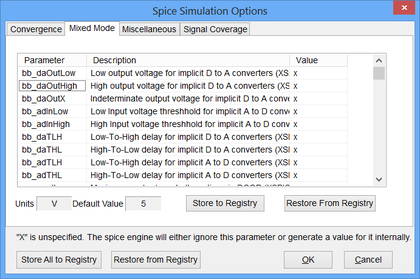
B2.Spice A/D allows you to mix digital and analog devices in the same circuit. To simulate the resulting circuit, B2.Spice places implicit A/D converters and/or D/A converters in your circuit behind the scenes. By default, it is assumed that the "1" or "High" digital state corresponds to a +5V analog voltage, while the "0" or "Low" digital state corresponds to a 0V analog voltage. You can change these conversion values depending the type of digital device technology you are using in your circuit. This can be done from the SPICE Simulation Options dialog. You can access this dialog from the Simulate Menu. Under the "Mixed Mode" tab of this dialog, you will see two parameters "bb_daOutLow" and "bb_daOutHigh" in the Parameters table with default values of 0 and 5, respectively. To change these values, click on the parameter value in the rightmost column of the table to highlight it and then type in a new value.
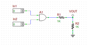
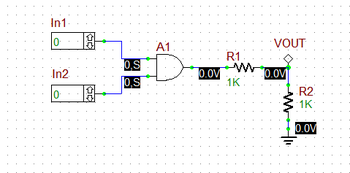
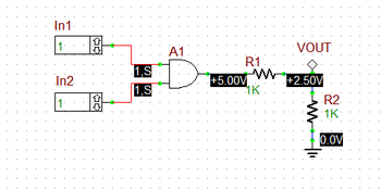
As a first step, let's try out a simple AND gate. Place two digital inputs and connect them to the AND gate. Connect the output of the AND gate to two 1k series resistors to form a voltage divider as shown in the opposite figure. Run a live simulation of this circuit and enable circuit animation by clicking the "Show Voltage Text" button of the Schematic Editor's Toolbar. When the two inputs are zero or at least one of them is zero, the output voltage is 0V. When both inputs are high, then the output voltage jumps to +5V as can be seen from the figures below.
Building a Basic D/A Converter
The following is a list of parts needed for this part of the tutorial lesson:
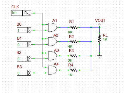
Four Digital Inputs: B0, B1, B2 and B3 (keyboard shortcut: N)
Four AND Gates: A1, A2, A3 and A4 (keyboard shortcut: A)
Digital Clock: CLK (keyboard shortcut: Alt+C)
5 Resistors: R1 = 8k, R2 = 4k, R3 = 2k, R4 = 1k, and RL = 1k (keyboard shortcut: R)
Voltage Probe Marker: VOUT (keyboard shortcut: Alt+L)
Place and connect all the parts as shown in the opposite figure. Note that the resistor R1 is twice the value of R2, and R2 is twice the value of R3, and so on. Set the period and pulse width of the digital clock CLK to 1ms and 500μs, respectively. The four digital inputs B0, B1, B2 and B3 together form a 4-bit digital word. The digital inputs are transferred to the resistors only during the high state of the clock due to the AND gates. The corresponding voltages are then added at the load resistor RL. It can be shown that the output voltage is given by:
[math] V_o = \frac {R_L V_h}{ R + (2^N - 1) R_L } \left( S_{N-1} 2^{N-1} + S_{N-2} 2^{N-2} + ... + S_1 2^1 + S_0 2^0 \right) [/math]
where vh is the high digital voltage, RL is the load resistor, R is the largest resistor value corresponding to the LSB input and Si represents the ith binary digit (S0 = LSB and SN-1 = MSB). For your circuit, N = 4, vh = +5V, RL = 1k, R = 8k, and you can write:
[math] V_o = \frac {5}{23} \left( 8S_3 + 4S_2 + 2S_1 + S_0 \right) [/math]
When all four digital inputs are low, the output voltage is zero. For "0001", the output voltage is 217.4mV, and for "0010", the output voltage is 434.8mV. For the largest possible 4-bit binary number "1111", the output voltage is 3.261V. Run a Transient Test of the basic D/A converter with the start and stop time set to 0 and 10ms, respectively, with a Step Ceiling of 1μs. Set different combinations of the four binary bits and plot the output voltage. Some of these graphs are shown in the figures below, and their results agree with the above analytical calculations.
Building an R-2R Ladder D/A Converter
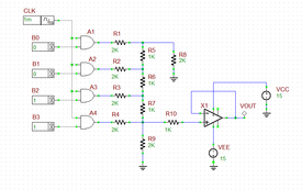
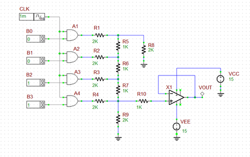
The basic D/A converter of the previous section required a wide range of resistor values. The R-2R ladder D/A Converter shown in the opposite figure requires only two values R and 2R connected successively in a ladder configuration. An Op-Amp voltage follower has been added at the output through a coupling resistor R10 as a buffer. Place and connect all the parts and use an LM741 Op-Amp for the voltage follower stage. The digital control circuit of this circuit is identical to the previous part with the period and pulse width of the digital clock CLK set to 1ms and 500μs, respectively. Run a Transient Test of the ladder D/A converter with the start and stop time set to 0 and 10ms, respectively, with a Step Ceiling of 1μs. Setting different combinations of the four binary bits, you can verify the operation of this D/A converter and get very similar results as in the previous case. The graph below shows the results for the case of the 4-bit binary number "1100".
Adding a Ripple Counter to Drive the Ladder D/A Converter
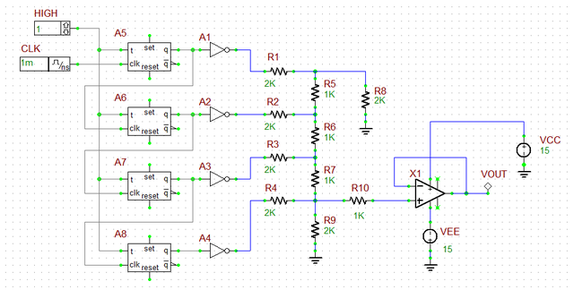
In Tutorial Lesson 11, you used JK flip-flops to build a 4-bit binary ripple counter. In the last part of this tutorial lesson, you will use the same type of binary counter to derive the input of your ladder D/A converter. However, this time you will use four Toggle flip-flops to build the ripple counter. All the T pins of the four flip-flops are set high. The clock in input to the first (LSB) flip-flop, while the clock of all the other flip-flops is fed by the Q-output of the previous stage. Four digital inverters are used at the outputs of the T-type flip-flops. The four outputs of the binary counter generate all the sixteen 4-bit binary numbers 0000, 0001, 0010, ..., 1110, 1111, in a cyclical manner. These digital inputs correspond to the analog voltage levels 0V, 210mV, 420mV, ..., 2.94V, 3.15V, respectively, or 210n V in general, where n = 0, 1, 2, ..., 15. Therefore, the analog output will successively increase from 0 to 3.15V with increments of 210mV at each time step. The, it drop down to zero and the discrete ramp starts all over again.
Set the period and pulse width of the digital clock CLK set to 1ms and 500μs, respectively. Run a Transient Test of the counter-driven ladder D/A converter with the start and stop time set to 0 and 50ms, respectively, with a Step Ceiling of 1μs. Note that you need 16 clock cycles to cover all the counter states. So you need to increase the simulation time. The output voltage graph is shown in the figure below.
