| Tutorial Project: Exploring an Integrated Circuit Voltage Comparator
|

|
|
Objective: In this project, you will analyze and examine an integrated circuit voltage comparator.
|
|
Concepts/Features:
- Bipolar Junction Transistor
- Zener Diode
- Live Simulation
- DC Sweep Test
|
|
Minimum Version Required: All versions
|
|
' Download Link: Analog Lesson 14 Download Link: Analog Lesson 14
|
What You Will Learn
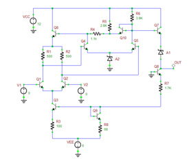
In this tutorial you will analyze a fairly complicated integrated circuit. The schematic of the LM710 Voltage Comparator is shown in the figure below. This device generates a binary output voltage fluctuating between -0.5V and +3.2V, which is TTL-compatible. So it may be used to generate binary signals for use in TTL logic circuits. The main objective of this tutorial lesson is to validate the simulation results of RF.Spice A/D through manual circuit analysis.
 The integrated circuit voltage comparator. |
Building the Voltage Comparator Circuit
The following is a list of parts needed for this project:
|
|
| Part Name
|
Part Type
|
Part Value
|
| V1 - V2
|
Voltage Source
|
1V
|
| VCC
|
Voltage Source
|
15V
|
| VEE
|
Voltage Source
|
-6V
|
| R1 - R2
|
Resistor
|
500
|
| R3
|
Resistor
|
100
|
| R4
|
Resistor
|
1.1k
|
| R5
|
Resistor
|
2.8k
|
| R6
|
Resistor
|
3.9k
|
| R7
|
Resistor
|
1.7k
|
| R8
|
Resistor
|
68
|
| Q1 - Q10
|
Generic NPN (BJT) Transistor
|
beta = 150
|
| A1 - A2
|
Generic Zener Diode
|
breakdown voltage = 6.2V
|
Place the parts listed above on the schematic and connect them as shown in the opposite figure. Alternatively, you may download the project file from our website. In this circuit, Q1 and Q2 together form an input differential amplifier pair, where Q3 provides a constant current source of the differential pair. Q5 provides an additional gain stage, while Q7 acts as a voltage follower buffer stage. Q9 and Q10 are equivalent to diodes. The Zener diodes A1 and A2 provide the necessary DC voltages for DC coupling and arrange proper output voltage levels. Make sure to change the forward beta parameter of the BJT transistors to 200 and set the breakdown voltage of the Zener diodes to 6.2V.
 |
When you change the parameters of an active device part like a diode or a transistor with a process (technology) model, the parameters of all the other parts in your circuit that share the same process model will also get updated automatically unless you make the part's model unique.
|
 Property dialog of the BJT Transistor. |
 Property dialog of the Zener Diode. |
Running a Live Simulation of the Voltage Comparator Circuit
Similar to the previous tutorial lessons, you will run live simulations of this circuit and will take advantage of RF.Spice's "Live Parameters" and "Circuit Animation" features. While the simulation is running, you will change the input voltage values and examine the circuit's output response.
At first, you will simulate the comparator circuit at its quiescent point when a zero differential input voltage, which is the case when V1 = V2 = 1V. The animated node voltages and branch currents are shown in the following figures. The output voltage in this case is about 1.2V.
 Reading of node voltages when V1 = V2 = 0V. |
 Reading of branch currents when V1 = V2 = 0V. |
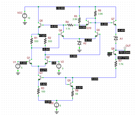
Next, you will examine two cases when the input differential voltage is sufficiently positive or negative. For the first case, set V1 = 5V and V2 = 0. For the second case, set V1 = 0 and V2 = 5V. You can change the source voltages in real time from the Toolbox's "Parameters Panel" while the simulation is still running. Follow the same procedure as in Tutorial Lessons 7 and 8. The figures below show the node voltages for the two cases. The output voltages are -0.752V and 3.11V in the two cases, respectively.
 Reading of node voltages when V1 = 5V and V2 = 0V. |
 Reading of node voltages when V1 = 0V and V2 = 5V. |
Verifying the Simulation Results
The LM710 comparator circuit shown in this figure has been analyzed extensively in Taub and Schilling's classic book "Digital Integrated Electronics". Here we will perform a similar analysis to verify RF.Spice's simulation results as you obtained in the previous part. The analysis is performed at the quiescent point with V1 = V2 = 1V. The base-emitter junction voltages for all transistors are assumed to be VBE = 0.75V. From the circuit figure, we can write VBE8 + 1700IE8 + VCE10 + 68IE10 - 6V = 0. Assuming that VBE8 = VCE10 = 0.75V and IE8 = IE10, we obtain IE8 = 2.54mA and VB3 = -5.07V. The simulated values for these quantities are 2.48mA and -5.03V, respectively. The emitter current of Q3 is found from the loop equation VB3 = VBE3 + 100IE3 -6V, which yields IE3 = 1.8mA compared to the simulated value of 1.78mA. This means that the emitter currents and therefore collector currents of Q1 and Q2 are 0.9mA each.
Next we will find the collector currents of Q4 and Q5. We have VC4 = VBE6 + 500IC1 + VBE4 + VZA2 = 0.75 + 500(0.0009) + 0.75 + 6.2 = 8.15V. The voltage drop across the two resistors (2.8k + 1.1k = 3.9k) at the collector of Q4 is 12 - 8.15 = 3.85V. Note that Q5 has a 3.9k resistor at its collector. Therefore, the collector currents of both Q4 and Q5 are equal: IC4 = IC5 = 3.85V / 3900Ω = 0.987mA. This leads to VC5 = VC4 = 8.15V. In this case, the diode-acting transistor Q9 does not conduct.
Finally, the output voltage is found to be Vo = VC5 - VBE7 - VZA1 = 8.15 - 0.75 - 6.2 = 1.2V, which almost the same as the simulated value of 1.19V.
Running a DC Sweep Test
As the final step of this tutorial lesson, you will run a DC Sweep Test of your voltage comparator circuit to better understand its binary output. Bring up the Test Panel, select the "DC Sweep" option and open the Test Setup Dialog. Enter the following sweep parameters:
|
|
| Source
|
V1
|
| Property
|
DC
|
| Start Value
|
-3.0V
|
| End Value
|
3.0V
|
| Step Value
|
20m
|
| Preset Graph Plots
|
v(out)
|
Note that for this test, you must set V2 = 0V. Then, changing the V1 level from -3V to +3V will cover both cases of positive and negative differential inputs. Run the basic DC Sweep Test, and you will get a response curve like the one shown in the opposite figure.
 DC response of the voltage comparator as a function of V1 level, when V2 = 0V. |
 Back to RF.Spice A/D Tutorial Gateway


