Advanced Tutorial Lesson 12: Exploring a 3-Bit A/D Converter Circuit
Contents
What You Will Learn
In this tutorial you will use SPICE's standard voltage-controlled switch to sample signals and will build and test sample-and-hold (S/H) circuits.
Testing a Voltage Comparator Integrated Circuit
The following is a list of parts needed for this part of the tutorial lesson:
| Part Name | Part Type | Part Value |
|---|---|---|
| V1 | Voltage Source | 2 |
| V2 | Voltage Source | 1 |
| VCC | DC Bias Voltage Source | 5 |
| R1 | Resistor | 2k |
| X1 | LM393 Differential Voltage Comparator | Defaults |
| VOUT | Voltage Probe Marker | N/A |
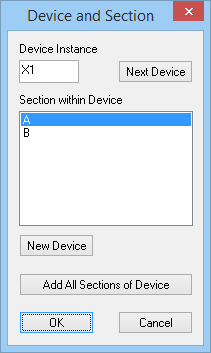
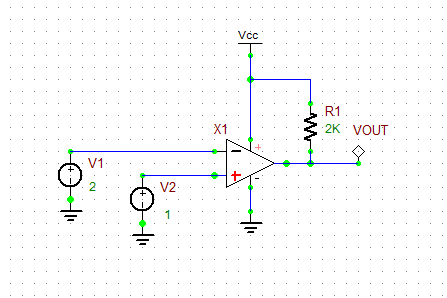
In Analog Tutorial Lesson 12, you analyzed the operation of an analog voltage comparator integrated circuit. In this project, you will use a commercial voltage comparator IC called LM393 manufactured by Texas Instruments. The DC bias voltage source Vcc determines the comparator's high output voltage. We choose +5V high state voltage for this project. You can access the IC either from Part Bin or using the menu item menu > Parts > Active Devices > Integrated Circuits > LM393 Differential Voltage Comparator. Each LM393 IC package contains two devices. When you place the part, a dialog opens up and asks you whether you want "Section A" or "Section B". If one has been used up earlier, only the other available section will show up in the list. The dialog also gives you options or buttons for New Device and Next Device.
Place and connect all the parts as shown in the figure below:
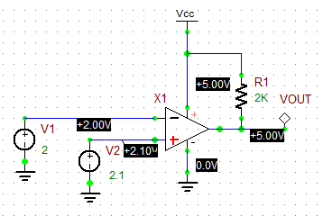
With V2 = 1V and V1 = 2V, run a live simulation of this circuit and enable Show Voltage Text. From the figures below, you can see that the output voltage is less than 0.1V or at "low state", because V2 < V1. Next, change the source voltage of V2 to 2.1V. This time, you will see the output voltage jump to +5V, which is the voltage of Vcc.
Building a Ladder A/D Converter
The following is a list of parts needed for this part of the tutorial lesson:
| Part Name | Part Type | Part Value |
|---|---|---|
| VS | Voltage Source | Value TBD |
| VPOS | Voltage Source | +1 |
| VNEG | Voltage Source | -1 |
| VCC | DC Bias Voltage Source | 5 |
| R1 - R8 | Resistor | 100 |
| R9 - R15 | Resistor | 2K |
| X1 - X7 | LM393 Differential Voltage Comparator | Defaults |
| A1 - A7 | 1-Bit A/D Conversion Bridge | Defaults, in_high = 4.5 |
| Out1 - Out7 | Digital Output | N/A |
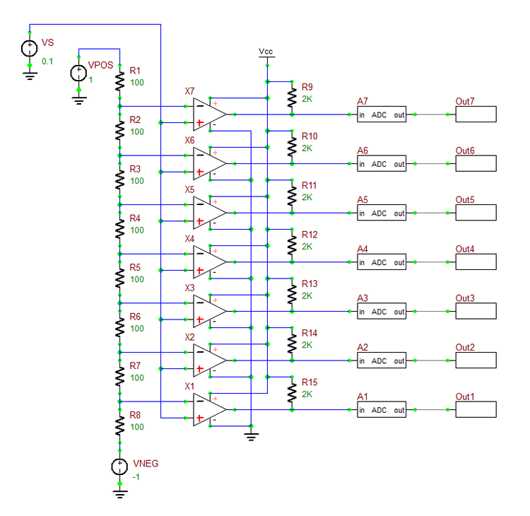
The voltage source VPOS and VNEG are set to the highest and lowest values of your analog signal, which are +1V and -1V, respectively. The resistive ladder network made up of R1 to R8 provides incremental voltages from -1V to +1V with successive steps of 0.25V. Therefore, you have 8 = 23 distinct voltage levels corresponding to 3 binary bits. VS is your analog signal source, whose voltage is compared to all these 8 distinct voltage levels. The outputs of the comparators are then converted to binary values using the 7 A/D bridges.
Place and connect all the part as shown in the figure below. When placing the LM393 parts, don't use the half-package devices and place all new devices.
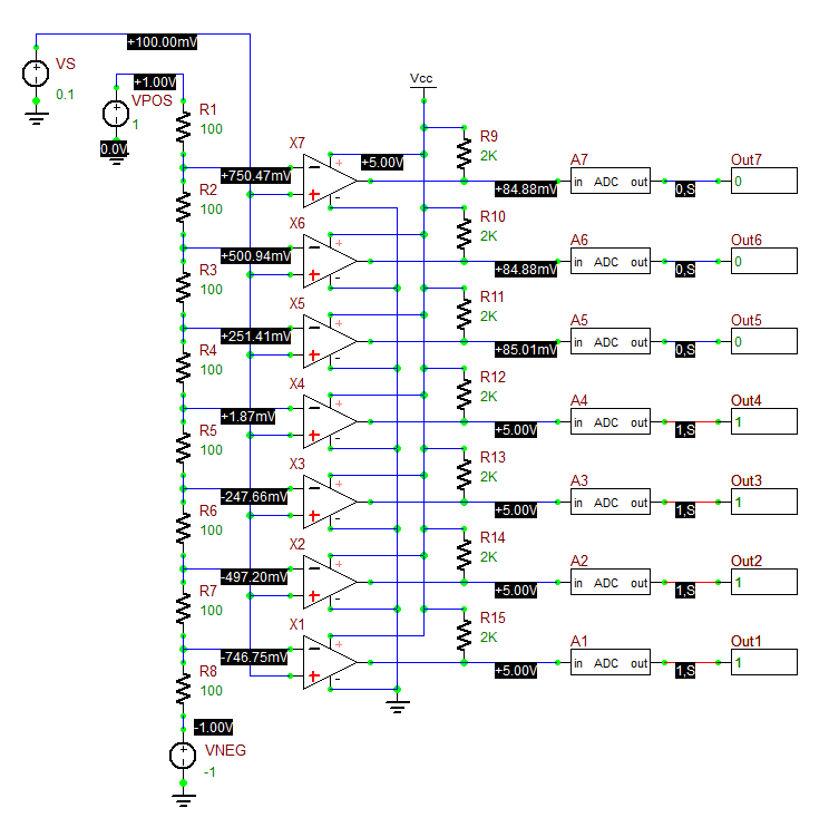
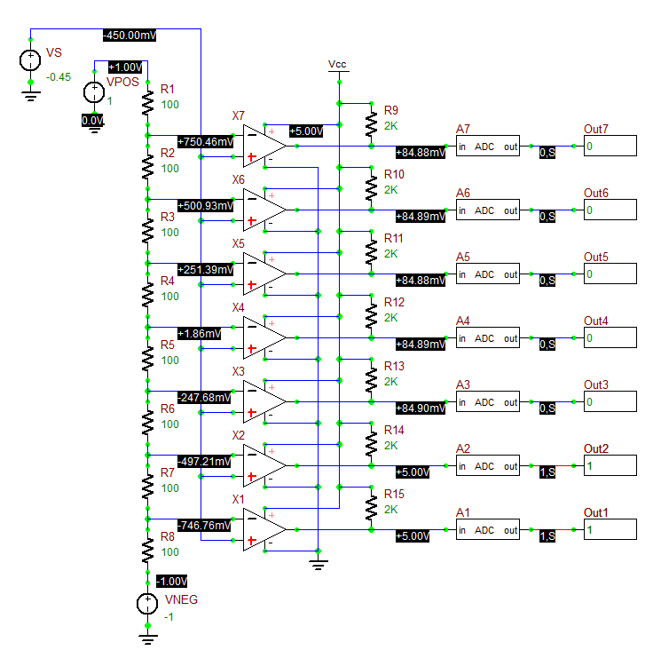
Set the voltage of the signal source VS to +0.45V and then -0.45V. Run live simulations of each case and observe the state of digital outputs:
Adding the Logic Decoder
The following is a list of parts needed for this part of the tutorial lesson:
| Part Name | Part Type | Part Value |
|---|---|---|
| VS | Voltage Source | Value TBD |
| VPOS | Voltage Source | +1 |
| VNEG | Voltage Source | -1 |
| VCC | DC Bias Voltage Source | 5 |
| R1 - R8 | Resistor | 100 |
| R9 - R15 | Resistor | 2K |
| X1 - X7 | LM393 Differential Voltage Comparator | Defaults |
| A1 - A6 | Generic XOR Gate | Defaults |
| A7 - A9 , A11 | Generic AND Gate | Defaults |
| A10 | Generic XNOR Gate | Defaults |
| A12 - A14 | Generic OR Gate | Defaults |
| B0 - B2 | Digital Output | N/A |
The outputs of the seven comparators are either +5V or less than 0.1V in all cases. In this section, you will add a logic decoder to convert the 7 digital outputs to a 3-bit digital word. The following table shows all the 8 distinct voltage levels, their corresponding signal voltage ranges and their associated 3-bit digital words:
| Signal Voltage Range | Voltage Level Index | B2 | B1 | B0 |
|---|---|---|---|---|
| -1V < VS < -0.75V | 0 | 0 | 0 | 0 |
| -0.75V < VS < -0.50V | 1 | 0 | 0 | 1 |
| -0.50V < VS < -0.25V | 2 | 0 | 1 | 0 |
| -0.25V < VS < 0V | 3 | 0 | 1 | 1 |
| 0V < VS < 0.25V | 4 | 1 | 0 | 0 |
| 0.25V < VS < 0.50V | 5 | 1 | 0 | 1 |
| 0.50V < VS < 0.75V | 6 | 1 | 1 | 0 |
| 0.75V < VS < 1V | 7 | 1 | 1 | 1 |
If we denote the outputs of the seven comparators X1 - X7 by c1 - c7, it is not difficult to verify the following relationships:
[math] b0 = \left( \left( (c1\oplus c2) \oplus (c3\oplus c4) \right) \oplus (c5\oplus c6) \right) \oplus c7 [/math]
[math] b1 = (c1. c2) \ . \left( \ (c3. c4) \bar{\oplus} (c5. c6) \ \right) [/math]
[math] b2 = (c4 + c5) + (c6 + c7) [/math]
where b0, b1 and b2 are the three bit of the output digital word.
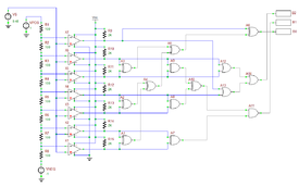
Place and connect all the parts as shown in the figure below. Note that you don't need the ADC bridges for this part because RF.Spice A/D automatically takes care of A/D conversions due to the presence of the logic gates in combination with the analog parts. You can use the circuit from the previous part, remove the ADC bridges and add all the new gates listed above.
Set various values for the signal voltage and run live simulations of your circuit. In the figure below, the voltage animation is shown for the cases VS = -0.17V and VS = +0.82V. Their corresponding digital words are 011 and 111, respectively.
