The Very Old Glossary of Signal Sources and Waveform Generation Blocks
Contents
- 1 AC/RF Current Source
- 2 AC/RF Voltage Source
- 3 AM Modulated Source
- 4 Analog Clock
- 5 Arbitrary Temporal Waveform Generator
- 6 Controlled One-Shot
- 7 Controlled Sine Wave Oscillator
- 8 Controlled Sources
- 9 Controlled Square Wave Oscillator
- 10 Controlled Triangle Wave Oscillator
- 11 Current Noise Source
- 12 Current Source
- 13 DC Bias Sources Vcc, Vee, Vdd, Vss
- 14 Finite Sequence Pulse Generator
- 15 Finite Sequence Random Pulse Generator
- 16 FM Modulated Source
- 17 Impulse Generator
- 18 Linear Current-Controlled Current Source (CCCS)
- 19 Linear Current-Controlled Voltage Source (CCVS)
- 20 Linear Voltage-Controlled Current Source (VCCS)
- 21 Linear Voltage-Controlled Voltage Source (VCVS)
- 22 Nonlinear Dependent Sources
- 23 Piecewise Linear (PWL) Controlled Source
- 24 PM Modulated Source
- 25 Pulse Generator
- 26 Quadrature Harmonic Wave Generator
- 27 Ramp Generator
- 28 Random Digitized Signal Generator
- 29 Random Noise Generator
- 30 Random Pulse Generator
- 31 Sine Wave Chirp Generator
- 32 Square Wave Chirp Generator
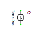
- 33 Temperature-Dependent Current Source
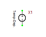
- 34 Temperature-Dependent Voltage Source
- 35 Triangular Wave Chirp Generator
- 36 Triangular Wave Generator
- 37 Voltage Noise Source
- 38 Voltage Source
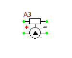
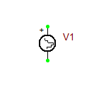
AC/RF Current Source
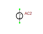
This is a simplified version of the standard Current Source, in which the AC "Use" box has been checked by default. Therefore, it is ready to be used for AC frequency sweep. Note that for AC frequency sweep, you do not need to specify the frequency.
Parameters:
| NAME | PARAMETER | UNIT | DEFAULT | NOTES |
|---|---|---|---|---|
| VA | peak current amplitude | A | 1 | required |
| Freq | frequency | Hz | 1 | required |
| Phase | phase | deg | 0 | |
| offset | DC offset for small-signal current | A | 0 |
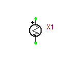
AC/RF Voltage Source
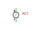
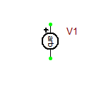
This is a simplified version of the standard Voltage Source, in which the AC "Use" box has been checked by default. Therefore, it is ready to be used for AC frequency sweep. Note that for AC frequency sweep, you do not need to specify the frequency.
Parameters:
| NAME | PARAMETER | UNIT | DEFAULT | NOTES |
|---|---|---|---|---|
| VA | peak voltage amplitude | V | 1 | required |
| Freq | frequency | Hz | 1 | required |
| Phase | phase | deg | 0 | |
| offset | DC offset for small-signal voltage | V | 0 |
AM Modulated Source
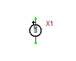
This is a voltage source with a single-tone amplitude modulated waveform. The AM modulation index MDI is defined as the ratio of maximum amplitude deviation to maximum signal amplitude.
Parameters:
| NAME | PARAMETER | UNIT | DEFAULT | NOTES |
|---|---|---|---|---|
| V0 | offset | V | 0 | |
| VA | amplitude | V | 1 | |
| FC | carrier frequency | Hz | 1 | required |
| MDI | modulation index | - | 0 | required |
| FS | signal frequency | Hz | 1 | required |
Analog Clock
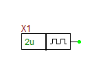
This is a periodic pulse generator with a default 0V low output level and a default 5V high output level.
Parameters:
| NAME | PARAMETER | UNIT | DEFAULT | NOTES |
|---|---|---|---|---|
| delay | delay time | sec | 0 | |
| rise | rise time | sec | 0.1n | |
| fall | fall time | sec | 0.1n | |
| pulse_wid | clock pulse width | sec | 1u | required |
| period | clock period | - | 2u | required |
| out_low | low output voltage level | V | 0 | |
| out_high | high output voltage level | V | 5 |
Arbitrary Temporal Waveform Generator
This is a voltage source with an arbitrary waveform defined by a mathematical expression. You have to open the subcircuit model dialog by clicking the View Subcircuit button and edit its text. Enter any mathematical expression in the variable "v(t)" standing for time.
Examples:
- v(t) is equivalent to f(t) = t.
- 0.1*(v(t))^2 is equivalent to f(t) = 0.1t^2.
- sin(2*pi*v(t)) is equivalent to f(t) = sin(2πt).
Parameters:
| NAME | PARAMETER | UNIT | DEFAULT | NOTES |
|---|---|---|---|---|
| Tmax | maximum signal duration | sec | 1e6 | required |
Controlled One-Shot
This is an eight-terminal function generator with a single pulse output. The pulse width is controlled by an input voltage. The functional dependency of the output pulse width on the input voltage is piecewise linear and is defined as a two-dimensional table similar to a piecewise linear (PWL) controlled source. In the "pulse width vs. voltage" curve, the array "cntl_array" defines voltage values in Volts and the array "pw_array" defines the corresponding pulse width values in seconds.
The generation of the output pulse is triggered either on the rising or falling edge of a clock input.
Model Identifier: oneshot
Netlist Format:
A<device_name> %vd(<clk_pin> <clk_ref_pin>) %vd(<cntl_in_pin> <cntl_in_ref_pin>) %vd(<clear_pin> <clear_ref_pin>) %vd(<out_pin> <out_ref_pin>) <model_name>
.model <model_name> oneshot {<param1 = value> < param2 = value> ...}
Example:
A1 %vd(1 5) %vd(2 6) %vd(3 7) %vd(4 8) one_shot
.model one_shot oneshot cntl_array = [0.0] pw_array = [1u] rise_time = 1n
Parameters:
| NAME | PARAMETER | UNIT | DEFAULT | NOTES |
|---|---|---|---|---|
| Clk_trig | clock trigger value | V | 0.5 | |
| Pos_edge_trig | positive/negative edge trigger switch | - | True | |
| Cntl_array | control array | V | [0.0] | required |
| Pw_array | pulse width array | sec | [1u] | required |
| Out_low | output low value | V | 0.0 | |
| Out_high | output high value | V | 1.0 | |
| Delay | output delay from trigger | sec | 1.0e-9 | |
| Rise_time | output rise time | sec | 1.0e-9 | |
| Fall_time | output fall time | sec | 1.0e-9 |
Controlled Sine Wave Oscillator
This is a four-terminal function generator with a sinusoidal wave output, whose frequency is controlled by an input voltage. The functional dependency of the output frequency on the input voltage is piecewise linear and is defined as a two-dimensional table similar to a piecewise linear (PWL) controlled source. In the "frequency vs. voltage" curve, the array "cntl_array" defines voltage values in Volts and the array "freq_array" defines the corresponding frequencies in Hz. This function has parameterizable values of low and high peak output voltage.
Model Identifier: sine
Netlist Form:
A<device_name> %vd(<cntl_in_pin> <cntl_in_ref_pin>) %vd(<out_pin> <out_ref_pin>) <model_name>
.model <model_name> sine cntl_array = [<value1> <value2>] freq_array = [<value1> <value2>] {<param1 = value> < param2 = value> ...}
Example:
A1 %vd(1 3) %vd(2 4) sine
.model sine sine cntl_array = [0 1] freq_array = [1 1000]
Parameters:
| NAME | PARAMETER | UNIT | DEFAULT | NOTES |
|---|---|---|---|---|
| Cntl_array | control array | V | [0 1] | required |
| Freq_array | frequency array | Hz | [1 1000] | required |
| Out_low | output peak low value | V | -1.0 | |
| Out_high | output peak high value | V | 1.0 |
Controlled Sources
Circuits can contain linear dependent sources characterized by one of the following equations (where g, e, f, and h are constants representing transconductance, voltage gain, current gain, and transresistance, respectively):
iout = g vin vout = e vin iout = f iin vout = h iin
For further information, refer to:
Linear Current Controlled Current Source (CCCS)
Linear Voltage Controlled Current Source (VCCS)
Linear Current Controlled Voltage Source (CCVS)
Linear Voltage Controlled Voltage Source (VCVS)
Controlled Square Wave Oscillator
This is a four-terminal function generator with a square wave output, whose frequency is controlled by an input voltage. The functional dependency of the output frequency on the input voltage is piecewise linear and is defined as a two-dimensional table similar to a piecewise linear (PWL) controlled source. In the "frequency vs. voltage" curve, the array "cntl_array" defines voltage values in Volts and the array "freq_array" defines the corresponding frequencies in Hz.
Model Identifier: square
Netlist Format:
A<device_name> %vd(<cntl_in_pin> <cntl_in_ref_pin>) %vd(<out_pin> <out_ref_pin>) <model_name>
.model <model_name> square cntl_array = [<value1> <value2>] freq_array = [<value1> <value2>] {<param1 = value> < param2 = value> ...}
Example:
A1 %vd(1 3) %vd(2 4) square
.model square square cntl_array = [0 1] freq_array = [1 1000]
Parameters:
| NAME | PARAMETER | UNIT | DEFAULT | NOTES |
|---|---|---|---|---|
| Cntl_array | control array | V | [0 1] | required |
| Freq_array | frequency array | Hz | [0 1000] | required |
| Out_low | output peak low value | V | -1.0 | |
| Out_high | output peak high value | V | 1.0 | |
| Duty_cycle | Duty cycle | - | 0.5 | |
| Rise_time | Output rise time | sec | 1.0e-9 | |
| Fall_time | Output fall time | sec | 1.0e-9 |
Controlled Triangle Wave Oscillator
This is a four-terminal function generator with a triangle wave output, whose frequency is controlled by an input voltage. The functional dependency of the output frequency on the input voltage is piecewise linear and is defined as a two-dimensional table similar to a piecewise linear (PWL) controlled source. In the "frequency vs. voltage" curve, the array "cntl_array" defined voltage values in Volts and the array "freq_array" defines the corresponding frequencies in Hz.
Model Identifier: triangle
Netlist Format:
A<device_name> %vd(<cntl_in_pin> <cntl_in_ref_pin>) %vd(<out_pin> <out_ref_pin>) <model_name>
.model <model_name> tirangle cntl_array = [<value1> <value2>] freq_array = [<value1> <value2>]{<param1 = value> < param2 = value> ...}
Example:
A1 %vd(1 4) %vd(2 3) triangle
.model triangle triangle cntl_array = [0 1] freq_array = [1 1000]
Parameters:
| NAME | PARAMETER | UNIT | DEFAULT | NOTES |
|---|---|---|---|---|
| Cntl_array | control array | V | [0 1] | required |
| Freq_array | frequency array | Hz | [0 1000] | required |
| Out_low | output peak low value | V | -1.0 | |
| Out_high | output peak high value | V | 1.0 | |
| Rise_duty | Rise time duty cycle | 0.5 |
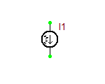
Current Noise Source
This is a current noise generator characterized by a spectral density and corner frequency. You have to click the Edit Model... button to access the parameters of this device.
Parameters:
| NAME | PARAMETER | UNIT | DEFAULT | NOTES |
|---|---|---|---|---|
| En | noise current | A/√Hz | 1p | required |
| freq | noise corner frequency | Hz | 100 | required |
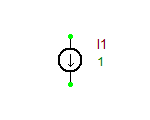
Current Source
Current source has a DC value, a transient behavior, an AC behavior, and distortion parameters. The transient type, AC parameters, and distortion parameters are defined on the first tab of the source's property dialog. The transient expression can be a pulse, sinusoid, exponential, or piecewise linear. The DC value of a current source is its initial transient value. For a source with a sinusoidal transient behavior, for example, the DC value will be equal to its transient offset current. The AC parameters are magnitude and phase. These are used during the AC Frequency Sweep analysis. The distortion parameters, two sets of magnitude and phase, are used during the distortion analysis. The AC and distortion parameters are defined on the second tab of the source's property dialog.
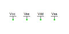
DC Bias Sources Vcc, Vee, Vdd, Vss
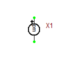
These are simple 1-pin DC voltage sources. Vcc and Vdd provide a positive voltage, while Vee and Vss provide a negative voltage
Parameters:
| NAME | PARAMETER | UNIT | DEFAULT | NOTES |
|---|---|---|---|---|
| vcc | bias voltage | V | +15 | required |
| vee | bias voltage | V | -15 | required |
| vdd | bias voltage | V | +15 | required |
| vss | bias voltage | V | -15 | required |
Finite Sequence Pulse Generator
This is a voltage source that generates a pulse train of finite duration oscillating between zero and a user defined maximum voltage level.
Parameters:
| NAME | PARAMETER | UNIT | DEFAULT | NOTES |
|---|---|---|---|---|
| T | pulse period | sec | 1m | required |
| w | pulse width | sec | 0.5m | required |
| n | number of pulses | - | 5 | |
| rise_time | pulse rise time | sec | 0 | |
| fall_time | pulse fall time | sec | 0 | |
| max_val | maximum output voltage level | V | 1 | |
| start | start time | sec | 0 |
Finite Sequence Random Pulse Generator
This is a voltage source that generates a finite sequence of random pulses with a user defined number of random levels. By default, both the pulse amplitude and pulse width are randomized. You have the option to fix either of these parameters.
Parameters:
| NAME | PARAMETER | UNIT | DEFAULT | NOTES |
|---|---|---|---|---|
| period | period | sec | 1 | required |
| duty_cycle | pulse duty cycle | - | 0.5 | required |
| random_amp | 1 for random amplitude, 0 otherwise | - | 1 | |
| random_wid | 1 for random pulse width, 0 otherwise | - | 1 | |
| n_rand | number of random levels | - | 10 | |
| rise_time | pulse rise time | sec | 0 | |
| fall_time | pulse fall time | sec | 0 | |
| max_val | maximum output voltage level | V | 1 | |
| n_val | number of random pulses | - | 5 | |
| start | start time | sec | 0 |
FM Modulated Source
This is a voltage source with a single-tone frequency modulated waveform. The FM modulation index MDI is defined as the ratio of maximum frequency deviation to maximum signal amplitude.
Parameters:
| NAME | PARAMETER | UNIT | DEFAULT | NOTES |
|---|---|---|---|---|
| V0 | offset | V | 0 | |
| VA | amplitude | V | 1 | |
| FC | carrier frequency | Hz | 1 | required |
| MDI | modulation index | - | 0 | required |
| FS | signal frequency | Hz | 1 | required |
Impulse Generator
This is a voltage source that generates a periodic impulse train with oscillating between zero and a user defined maximum voltage level.
Parameters:
| NAME | PARAMETER | UNIT | DEFAULT | NOTES |
|---|---|---|---|---|
| T | impulse period | sec | 1u | required |
| duty_cycle | impulse duty cycle | - | 0.01 | required |
| max_val | maximum output voltage level | V | 1 | |
| delay | delay time | sec | 0 |
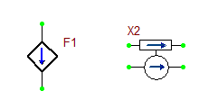
Linear Current-Controlled Current Source (CCCS)
The CCCS is a current source whose current is directly proportional to the current across a controlling Ammeter or a voltage source. There are two versions: two-terminal and four-terminal. For the two-terminal device, you must specify the name of the controlling Ammeter or voltage source, as well as the current gain, which has a default value of one. The four-terminal device already provides nodes for a controlling ammeter, and you just specify the current gain.
Model Identifier: cccs
Netlist Format:
F<device_name> <N+> <N-> <controlling_device_name> <value>
Example:
F1 1 0 V1 1.0
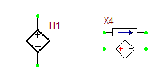
Linear Current-Controlled Voltage Source (CCVS)
The CCVS is a voltage source whose voltage is directly proportional to the current through a controlling ammeter or a voltage source. There are two versions: two-terminal and four-terminal. For the two-terminal device, you must specify the name of the controlling Ammeter or voltage source, as well as the trans-resistance gain, which has a default value of one. The four-terminal device already provides nodes for a controlling ammeter, and you just specify the trans-resistance gain.
Model Identifier: ccvs
Netlist Format:
H<device_name> <N+> <N-> <controlling_device_name> <value>
Example:
H1 1 0 V1 1.0
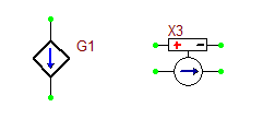
Linear Voltage-Controlled Current Source (VCCS)
The VCCS is a current source whose current is directly proportional to the voltage across a controlling voltmeter or the voltage between two circuit nodes. There are two versions: two-terminal and four-terminal. For the two-terminal device, you must specify the name of the controlling voltmeter or the two controlling nodes, as well as the trans-conductance gain, which has a default value of one. The four-terminal device already provides nodes for a controlling voltmeter, and you just specify the trans-conductance gain.
Model Identifier: vccs
Netlist Format:
G<device_name> <N+> <N-> <NC+> <NC-> <value>
Example:
G1 1 0 2 0 1.0
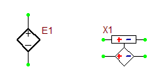
Linear Voltage-Controlled Voltage Source (VCVS)
The VCVS is a voltage source whose voltage is directly proportional to the voltage across a controlling voltmeter of the voltage between two circuit nodes. There are two versions: two-terminal and four-terminal. For the two-terminal device, you must specify the name of the controlling voltmeter or the two controlling nodes, as well as the voltage gain, which has a default value of one. The four-terminal device already provides nodes for a controlling voltmeter, and you just specify the voltage gain.
Model Identifier: vcvs
Netlist Format:
E<device_name> <N+> <N-> <NC+> <NC-> <value>
Example:
E1 1 0 2 0 1.0
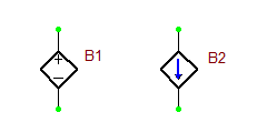
Nonlinear Dependent Sources
Nonlinear dependent (arbitrary) sources use an equation or mathematical expression to describe their behavior. One and only one of the two forms: V=<expr> or I=<expr> must be given.
Netlist Format:
B<device_name> v = <expression>
B<device_name> i = <expression>
Examples:
v = I(v1) + 3* I(v2)
I = v(i1) + 3* v(2) + 5 * v(3) ^2
The first example is a current-controlled voltage source. The v on the left side of the equation indicates that it is a voltage source. I(v1) and I(v2) are the currents through voltage sources named v1 and v2, respectively.
The second example is a voltage-controlled current source. v(2) and v(3) represents the voltages at nodes 2 and 3, respectively, and v(i1) represents the voltage across a current source named i1.
The following mathematical functions defined for real variables can be used in the expressions:
abs, acos, acosh, asin, asinh, atan, atanh, cos, cosh, exp, ln, log, sin, sinh, sqrt, tan.
The function "u" is the unit step and "uramp" is the integral of the unit step. The unit step is one if its argument is greater than zero and zero if its argument is less than zero. The ramp function (uramp) is 0 for argument values less than zero and equal to the argument for argument values greater than zero.
The following operators are permissible: +, -, *, /, ^, and unary-.
To get time into an expression, integrate the current from a constant current source with a capacitor and use the voltage across the capacitor.
Piecewise Linear (PWL) Controlled Source
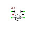
The Piecewise Linear (PWL) Controlled Source is a single-input and single-output function generator whose output is not necessarily linear for all input values. Instead, it follows an I/O relationship that is specified by the x_array and y_array coordinates. The x_array and y_array values represent vectors of coordinate points on the x and y axes, respectively. The x_array values are progressively increasing input coordinate points, and the associated y_array values represent the outputs at those points. There may be as few as two pairs specified, or as many as memory and simulation speed allow.
In order to fully specify outputs for values of Vin outside of the bounds of the PWL function, the PWL controlled source model extends the slope found between the lowest two coordinate pairs and the highest two coordinate pairs. This has the effect of making the transfer function completely linear for Vin less than x_array[0] and Vin greater than x_array[n]. It also has the potentially subtle effect of unrealistically causing an output to reach a very large or small value for large inputs. You should thus keep in mind that the PWL Source does not inherently provide a limiting capability.
In order to diminish the potential for divergence of simulations when using the PWL block, a form of smoothing around the x_array and y_array coordinate points is necessary. This is due to the iterative nature of the simulator and its reliance on smooth first derivatives of transfer functions in order to arrive at a matrix solution. Consequently, the two parameters "input_domain" and "fraction" are included to allow you some control over the amount and nature o the smoothing performed.
Fraction is a switch that is either TRUE or FALSE. When TRUE (the default setting), the simulator assumes that the specified input_domain value is to be interpreted as a fractional figure. Otherwise, it is interpreted as an absolute value. Thus, if fraction = TRUE and input_domain = 0.10, the simulator assumes that the smoothing radius about each coordinate point is to be set equal to 10% of the length of either the x_array segment above each coordinate point, or the x_array segment below each coordinate point. The specific segment length chosen will be the smallest of these two for each coordinate point.
If fraction = FALSE and input_domain = 0.10, then the simulator will begin smoothing the transfer function at 0.10 volts (or amperes) below each x_array coordinate and will continue the smoothing process for another 0.10 volts (or amperes) above each x_array coordinate point.
Model Identifier: pwl
Netlist Format:
A<device_name> %vd(<in_pin> <in_ref_pin>) %vd(<out_pin> <out_ref_pin>) <model_name>
.model <model_name> pwl x_array = [<value1> <value2> ...] y_array = [<value1> <value2> ...] {<param1 = value> < param2 = value> ...}
Example:
A1 %vd(2 3) %vd(1 4) pwl .model pwl pwl x_array = [0 1] y_array = [0 1]
Parameters:
| NAME | PARAMETER | UNIT | DEFAULT | NOTES |
|---|---|---|---|---|
| x_array | x-element array | V | [0 1] | required |
| y_array | y-element array | V | [0 1] | required |
| input_domain | input smoothing domain | - | 0.01 | |
| fraction | smoothing %/abs switch | - | True |
PM Modulated Source
This is a voltage source with a single-tone phase modulated waveform. The PM modulation index MDI is defined as the ratio of maximum phase deviation to maximum signal amplitude.
Parameters:
| NAME | PARAMETER | UNIT | DEFAULT | NOTES |
|---|---|---|---|---|
| V0 | offset | V | 0 | |
| VA | amplitude | V | 1 | |
| FC | carrier frequency | Hz | 1 | required |
| MDI | modulation index | - | 0 | required |
| FS | signal frequency | Hz | 1 | required |
Pulse Generator
This is a voltage source that generates a periodic pulse train with user defined low and high voltage levels.
Parameters:
| NAME | PARAMETER | UNIT | DEFAULT | NOTES |
|---|---|---|---|---|
| fo | frequency | Hz | 1Meg | required |
| duty_cycle | pulse duty cycle | - | 0.5 | required |
| delay | delay time | sec | 0 | |
| rise_time | pulse rise time | sec | 0 | |
| fall_time | pulse fall time | sec | 0 | |
| out_low | low output voltage level | V | -1 | |
| out_high | high output voltage level | V | +1 |
Quadrature Harmonic Wave Generator
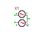
This is a 3-pin voltage source that generates two sinusoidal wave outputs with a 90° phase difference.
Parameters:
| NAME | PARAMETER | UNIT | DEFAULT | NOTES |
|---|---|---|---|---|
| fo | frequency | Hz | 1Meg | required |
| max_val | maximum output voltage level | V | 1 | |
| Vo | offset DC voltage | V | 0 | |
| Td | delay time | sec | 0 |
Ramp Generator
This is a voltage source that generates a periodic ramp also known as a sawtooth waveform with user defined low and high voltage levels. You can define either an up-ramp or a down-ramp.
Parameters:
| NAME | PARAMETER | UNIT | DEFAULT | NOTES |
|---|---|---|---|---|
| T | ramp period | sec | 1m | required |
| out_low | low output voltage level | V | -1 | |
| out_high | high output voltage level | V | +1 | |
| ramp_type | 0 for up-ramp, 1 for down-ramp | - | 0 |
Random Digitized Signal Generator
This is a voltage source that generates a periodic random digitized signal with a user defined number of random levels.
Parameters:
| NAME | PARAMETER | UNIT | DEFAULT | NOTES |
|---|---|---|---|---|
| period | sampling period | sec | 1 | required |
| n_rand | number of random levels | - | 10 | |
| max_val | maximum output voltage level | V | 1 |
Random Noise Generator
This is a periodic noise generator with user defined peak-to-peak amplitude fluctuation.
Parameters:
| NAME | PARAMETER | UNIT | DEFAULT | NOTES |
|---|---|---|---|---|
| vpp | peak-to-peak amplitude | V | 0.1 | required |
| offset | offset voltage | V | 0 | |
| period | period | sec | 1m | required |
Random Pulse Generator
This is a voltage source that generates a periodic random pulse train with a user defined number of random levels. By default, both the pulse amplitude and pulse width are randomized. You have the option to fix either of these parameters.
Parameters:
| NAME | PARAMETER | UNIT | DEFAULT | NOTES |
|---|---|---|---|---|
| period | period | sec | 1 | required |
| duty_cycle | pulse duty cycle | - | 0.5 | required |
| random_amp | 1 for random amplitude, 0 otherwise | - | 1 | |
| random_wid | 1 for random pulse width, 0 otherwise | - | 1 | |
| n_rand | number of random levels | - | 10 | |
| rise_time | pulse rise time | sec | 0 | |
| fall_time | pulse fall time | sec | 0 | |
| max_val | maximum output voltage level | V | 1 |
Sine Wave Chirp Generator
This is a voltage source that generates a sine wave output with sawtooth chirp modulation.
Parameters:
| NAME | PARAMETER | UNIT | DEFAULT | NOTES |
|---|---|---|---|---|
| period | chirp period | sec | 1u | required |
| freq_low | lower frequency value | Hz | 10Meg | required |
| freq_high | higher frequency value | Hz | 20Meg | required |
| max_val | maximum output voltage level | V | 1 | |
| chirp_type | 0 for up-chirp, 1 for down-chirp | - | 0 |
Square Wave Chirp Generator
This is a voltage source that generates a pulse train or square wave output with sawtooth chirp modulation.
Parameters:
| NAME | PARAMETER | UNIT | DEFAULT | NOTES |
|---|---|---|---|---|
| period | chirp period | sec | 1u | required |
| freq_low | lower frequency value | Hz | 10Meg | required |
| freq_high | higher frequency value | Hz | 20Meg | required |
| out_low | output lower limit | V | -1 | |
| out_high | output higher limit | V | +1 | |
| chirp_type | 0 for up-chirp, 1 for down-chirp | - | 0 |
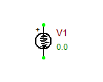
Temperature-Dependent Current Source
This is a current source whose current is an arbitrary function of the circuit temperature. You have to open the subcircuit model dialog by clicking the Edit Model... button and edit its text. Enter any mathematical expression in the variable "v(T)" standing for temperature. Note that the circuit temperature is set and controlled by the parameter "temp" in the Miscellaneous tab of the SPICE Simulation Options dialog.
Examples:
- v(T) is equivalent to f(T) = T.
- 1 + 0.1*(v(t))^2 is equivalent to f(T) = 1 + 0.1T.
Parameters:
None
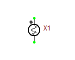
Temperature-Dependent Voltage Source
This is a voltage source whose voltage is an arbitrary function of the circuit temperature. You have to open the subcircuit model dialog by clicking the Edit Model... button and edit its text. Enter any mathematical expression in the variable "v(T)" standing for temperature. Note that the circuit temperature is set and controlled by the parameter "temp" in the Miscellaneous tab of the SPICE Simulation Options dialog.
Examples:
- v(T) is equivalent to f(T) = T.
- 1 + 0.1*(v(t))^2 is equivalent to f(T) = 1 + 0.1T.
Parameters:
None
Triangular Wave Chirp Generator
This is a voltage source that generates a triangular wave output with sawtooth chirp modulation.
Parameters:
| NAME | PARAMETER | UNIT | DEFAULT | NOTES |
|---|---|---|---|---|
| period | chirp period | sec | 1u | required |
| freq_low | lower frequency value | Hz | 10Meg | required |
| freq_high | higher frequency value | Hz | 20Meg | required |
| out_low | output lower limit | V | -1 | |
| out_high | output higher limit | V | +1 | |
| chirp_type | 0 for up-chirp, 1 for down-chirp | - | 0 |
Triangular Wave Generator
This is a voltage source that generates a triangular wave output oscillating between -A and A, where A is a user defined maximum voltage levels.
Parameters:
| NAME | PARAMETER | UNIT | DEFAULT | NOTES |
|---|---|---|---|---|
| fo | frequency | Hz | 1Meg | required |
| duty_cycle | pulse duty cycle | - | 0.5 | required |
| max_val | maximum output voltage level | V | 1 |
Voltage Noise Source
This is a voltage noise generator characterized by a spectral density and corner frequency. You have to click the Edit Model... button to access the parameters of this device.
Parameters:
| NAME | PARAMETER | UNIT | DEFAULT | NOTES |
|---|---|---|---|---|
| En | noise voltage | V/√Hz | 1n | required |
| freq | noise corner frequency | Hz | 100 | required |
Voltage Source
A voltage source has a DC value, a transient behavior, an AC behavior, and distortion parameters. The transient type, AC parameters, and distortion parameters are defined on the first tab of the source's property dialog. The transient expression can be a pulse, sinusoid, exponential, or piecewise linear. The DC value of a voltage source is its initial transient value. For a source with a sinusoidal transient behavior, for example, the DC value will be equal to its transient offset voltage. The AC parameters are magnitude and phase. These are used during the AC Frequency Sweep analysis. The distortion parameters, two sets of magnitude and phase, are used during the distortion analysis. The AC and distortion parameters are defined on the second tab of the source's property dialog.
