RF Tutorial Lesson 5: Designing Lumped and Distributed Microstrip Lowpass Filters
Analyzing Microstrip Lines, Discontinuities and Filters
Contents
Objective
In this tutorial, you will learn how to design and use microstrip lines and components. You will analyze a microstrip double-step and will utilize microstrip discontinuity models to improve the accuracy of your analysis. Then you will build and analyze a stepped-impedance microstrip lowpass filter based on a standard lumped LC filter design.
Designing Microstrip Lines
RF.Spice has a large number of physical line calculators and designers. You can access these tools from the Device Editor. Open RF.Spice's Device Editor either from its File Menu or using the keyboard shortcut "Ctrl+D". At the top of Device Editor's RF Menu, find "Microstrip Designer" and open it. For this project, you will use an FR-4 substrate of thickness h = 1.2mm, relative permittivity er = 4.5 and loss tangent tand = 0.02. To design a 50Ω microstrip line, enter these values into the designer dialog and set Z0 = 50. The corresponding width value is computed to be 2.3mm.
In order to verify your design, go back to the RF.Spice Workshop and place a "Microstrip Line" part on the schematic either using the RF Menu of Schematic Editor or using the keyboard shortcut "Alt+T". Open the part's property dialog and enter the parameters: w = 2.3mm, h = 1.2mm, er = 4.5, len = 20mm, tand = 0.02, as shown in the figure below. Terminate the line segment in a 50Ω resistor and ground both negative pins of the microstrip. Place a "Net" Marker called "IN" (keyboard shortcut: Alt+N) at the input of the microstrip segment. Run a Network Analysis of this simple circuit, with Port 1 defined between node IN and the ground. Set the frequency sweep to go from 100MHz to 6GHz with the linear steps of 100MHz. Choose the Smith Chart for your output data and run the test. You will see a Smith chart like the one shown below with all the frequency points overlaid at the center of the chart. This means that the input impedance of your circuit at Port 1 is Zin = 50Ω at all frequencies. This can happen only if the characteristic impedance of you transmission line segment perfectly matches your termination load.
Calculating Microstrip Line Parameters
Next, you will use the Device Editor's "Microstrip Calculator" to find the effective permittivity of your 50Ω microstrip line and its guide wavelength at 2GHz. Open the Line Calculator from the RF Menu of Device Editor. Enter the parameters: w = 2.3mm, h = 1.2mm, er = 4.5, len = 20mm, tand = 0.02, as shown in the opposite figure. In the other parts of this tutorial lesson you will use very wide and very narrow microstrip line segments. Repeat the same calculations for microstrip width values of 0.5mm and 5mm. The results are summarized in the table below.
| w | Z0 | εeff | Guide Wavelength λg at 2GHz |
|---|---|---|---|
| 2.3mm | 49.74Ω | 3.37 | 81.76mm |
| 0.5mm | 101.59Ω | 3.06 | 85.79mm |
| 5mm | 29.55Ω | 3.61 | 78.91mm |
Analyzing a Microstrip Double Step
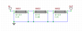
The characteristic impedance Z0 of a microstrip line is inversely proportional to its width as you saw in the previous section. When you connect two microstrip lines of different widths directly to each other, you create a transmission line discontinuity, which is called an impedance step. In this part of the tutorial lesson, you will analyze a circuit composed of two back-to-back 2.3mm-to-5mm and 5mm-to-2.3mm impedance steps with a 10mm-long, 5mm-wide, microstrip segment in between. You will use 50Ω input and output lines as shown in the opposite figure. A list of microstrip line segments is given in the table below. Place the parts and connect them as shown. Place two "Net" Markers called "IN" and "OUT" (keyboard shortcut: Alt+N) at the input and output of your circuit.
| Line Segment | w | len | Z0 |
|---|---|---|---|
| L1 | 2.3mm | 5mm | 50Ω |
| L2 | 5mm | 10mm | 30Ω |
| L3 | 2.3mm | 5mm | 50Ω |
Run a Network Analysis of the double step circuit, with Port 1 defined between node IN and the ground and Port 2 defined between node OUT and the ground . Set the frequency sweep to go from 100MHz to 6GHz with the linear steps of 10MHz. Instead of the Smith chart, this time choose a Cartesian graph type with amplitude only for the S-parameters.
You should get a graph like the one shown below.
Adding the Microstrip Step Discontinuity Models
The RF.Spice circuit shown above assumes that the microstrip line segments of different widths are directly connected to each other, and it ignores the effect of the step discontinuity. However, RF.Spice also provides a number of microstrip discontinuity models for you to increase the accuracy of your modeling. One of these devices is the two-port "Microstrip Step", which can be accessed from the Schematic Editor's RF Menu under the "Microstrip Discontinuities" group. The opposite figure shows the property dialog of this device. It assumes that the first microstrip (w1) at Port 1 is always wider than the second one (w2) at Port 2. Therefore, in order to use this device as a junction from segment L1 to L2, you have to flip it horizontally (keyboard shortcut: Ctrl+F) so that its Port 2 and 1 are connected to L1 and L2, respectively. Use another instance of the same device, but without flipping, as a junction from segment L2 to L3.
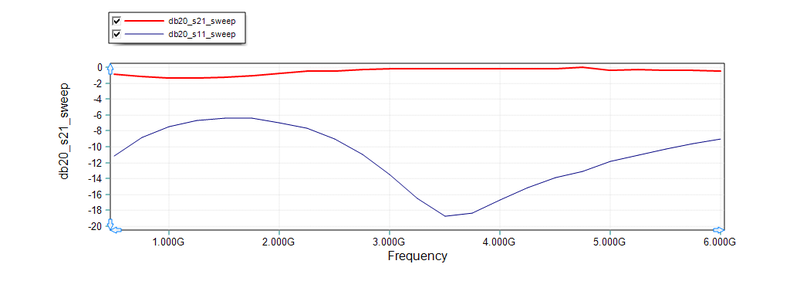
In order to see if the addition of the step discontinuity models has improved the simulation results, we have run a simulation of the physical structure using EM.Cube's Planar Module, EM.Picasso. The results for the s11 and s21 paramters over the same frequency range are shown in the figure below. Taking the full-wave electromagnetic simulation results as the baseline, you can see from the three S-parameter figures that the RF.Spice results including the discontinuity models better predict the dip of the s11-parameter than the simpler circuit without the discontinuity models.
Analyzing an LC Lowpass Filter
The following is a list of parts needed for this part of the tutorial lesson:
| Part | Value |
|---|---|
| C1 | 0.71pF |
| L1 | 4.96nH |
| C2 | 2.87pF |
| L2 | 7.96nH |
| C3 | 2.87pF |
| L3 | 4.96nH |
| C4 | 0.71pF |
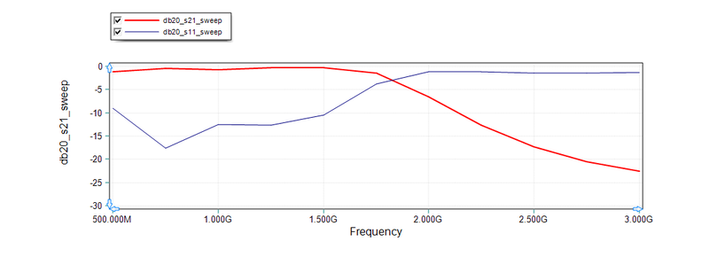
This is a classic Butterwoth LC lowpass filter with N = 7. The cutoff frequency of this filter is 2GHz and it attenuates to more than -20dB at 3GHz. Place the parts and connect them as a ladder filter. Mark the input and output of your lumped LC filter with two Net Markers: IN and OUT. Run a network analysis of this two-port circuit. Set the start and stop frequency of the sweep to 500MHz and 3GHz, respectively, with a linear step of 10MHz. Similar to the previous parts, generate a Cartesian, amplitude-only, graph of the S-parameters. The figure below shows the graph of s11- and s21 parameters. Note that a linear scale is used for frequency. The vertical axis is limited to -30dB and 0. Note that the s21 response drops by 3dB at the cutoff frequency fo = 2GHz.
Designing a Stepped Impedance Microstrip Lowpass Filter
A distributed microstrip version of the above ladder LC filter can be realized using consecutive low- and high-impedance line segments. It is well known that short segments of low- and high-impedance transmission lines behave like capacitive and inductive elements, respectively. Therefore, you will need four low-Z0 microstrip segments to replace the capacitors C1, C2, C3 and C4, and three high-Z0 microstrip segments to replace the inductors L1, L2 and L3. The transformations are based on the following equations:
[math] \beta l = \frac{ L R_0} {Z_{high}} [/math]
for inductors and
[math] \beta l = \frac{ C Z_{low}} {Z_{R_0}} [/math]
for capacitors. Here Zhigh and Zlow are the high and low characteristic impedances of the narrow and wide microstrip segments, respectively, and R0 is the reference impedance of the filter.
For this project, you will use 0.5mm-wide and 5mm-wide microstrip lines to realize Zhigh and Zlow, respectively. As you found earlier, these lines provide approximately 102Ω and 30Ω impedances, respectively. Using the above transformations, the following table for the segment lengths is obtained:
| Line Segment | w | len | Z0 |
|---|---|---|---|
| l1 | 3.3mm | 5mm | 29Ω |
| l2 | 8.4mm | 0.5mm | 102Ω |
| l3 | 13.4mm | 5mm | 29Ω |
| l4 | 13.5mm | 0.5mm | 102Ω |
| l5 | 13.4mm | 5mm | 29Ω |
| l6 | 8.4mm | 0.5mm | 102Ω |
| l7 | 3.3mm | 5mm | 29Ω |
Place and connect the above parts and mark the input and output of your circuit with two markers IN and OUT as shown in the above figure. Note how the negative pin (P1- and P2-) of all the parts have been grounded. Run a network analysis of your distributed filter circuit. Set the start and stop frequency of the sweep to 500MHz and 3GHz, respectively, with a linear step of 10MHz. Similar to the previous parts, generate a Cartesian, amplitude-only, graph of the S-parameters. The figure below shows the graph of s11- and s21 parameters. The horizontal and vertical axis scales have been set to match those of the lumped LC filter case for comparison.
In the above analysis, you assumed that the high-Z0 and low-Z0 sections are directly connected to each other. Your circuit configuration ignored the effect of the step discontinuities between the segment junctions. Next, you will include the discontinuity models in your circuit similar to what you did in the previous part of this tutorial lesson. However, this time you need three 5mm-to-0.5mm and two 0.5mm-to-5mm "Microstrip Step" parts. Remember again that in RF.Spice's microstrip model, w1 > w2. Therefore, you need to build the 0.5mm-to-5mm step by flipping the 5mm-to-0.5mm step horizontally. Similar to the microstrip line segment devices, you need to ground all the microstrip step devices, too. Forgetting to ground the RF parts properly may result in simulation failures. Run an AC Sweep Test of your new enhanced RF circuit and compare the results with the previous case. From the figures you can see that including the discontinuity models increase the slope of the roll-off part of the filter response. The previous circuit showed insertion loss values of -5dB and -17.5dB at 2GHz and 3GHz, respectively. After the inclusion of the five step discontinuity models, the new insertion loss values are -7dB and almost -20dB at 2GHz and 3GHz, respectively.
Finally, to validate the RF. Spice simulation results of your stepped-impedance microstrip filter, we have also included the full-wave simulation results for the same physical structure using EM.Cube's Planar MoM solver (EM.Picasso). As you can see from the figure below,


