EM.Picasso
Contents
An EM.Picasso Primer
EM.Picasso in a Nutshell
EM.Picasso® is a versatile planar structure simulator for modeling and design of printed antennas, planar microwave circuits, and layered periodic structures. EM.Picasso's simulation engine is based on a 2.5-D full-wave Method of Moments (MoM) formulation that provides the ultimate modeling accuracy and computational speed for open-boundary multilayer structures. It can handle planar structures with arbitrary numbers of metal layouts, slot traces, vertical interconnects and lumped elements interspersed among different substrate layers.
| |
EM.Picasso is the frequency-domain, full-wave Planar Module of EM.Cube, a comprehensive, integrated, modular electromagnetic modeling environment. EM.Picasso shares the visual interface, 3D parametric CAD modeler, data visualization tools, and many more utilities and features collectively known as CubeCAD with all of EM.Cube's other computational modules. |
![]() Click here to learn more about EM.Cube Modeling Environment.
Click here to learn more about EM.Cube Modeling Environment.
![]() Click here to learn more about the basic functionality of CubeCAD.
Click here to learn more about the basic functionality of CubeCAD.
An Overview of Planar Method of Moments
The Method of Moments (MoM) is a rigorous, full-wave numerical technique for solving open boundary electromagnetic problems. Using this technique, you can analyze electromagnetic radiation, scattering and wave propagation problems with relatively short computation times and modest computing resources. The method of moments is an integral equation technique; it solves the integral form of Maxwell’s equations as opposed to their differential forms that are used in the finite element or finite difference time domain methods.
In EM.Picasso, the background structure is a planar layered substrate that consists of one or more laterally infinite material layers always stacked along the Z-axis. In other words, the dimensions of the layers are infinite along the X and Y axes. Your substrate can be a dielectric half-space, or a single conductor-backed dielectric layer (as in microstrip components or patch antennas), or simply the unbounded free space, or any arbitrary multilayer stack-up configuration. In the special case of a free space substrate, EM.Picasso behaves similar to EM.Libera's Surface MoM simulator. Metallic traces are placed at the boundaries between the substrate or superstrate layers. These are modeled by perfect electric conductor (PEC) traces or conductive sheet traces of finite thickness and finite conductivity. Some layers might be separated by infinite perfectly conducting ground planes. The two sides of a ground plane can be electromagnetically coupled through one or more slots (apertures). Such slots are modeled by magnetic surface currents. Furthermore, the metallic traces can be interconnected or connected to ground planes using embedded objects. Such objects can be used to model circuit vias, plated-through holes or dielectric inserts. These are modeled as volume polarization currents.
In a planar MoM simulation, the unknown electric and magnetic currents are discretized as a collection of elementary currents with small finite spatial extents. As a result, the governing integral equations reduce to a system of linear algebraic equations, whose solution determines the amplitudes of all the elementary currents defined over the planar structure's mesh. Once the total currents are known, you can calculate the fields everywhere in the structure.
![]() Click here to learn more about the Theory of Planar Method of Moments.
Click here to learn more about the Theory of Planar Method of Moments.
Advantages & Limitations of EM.Picasso's Planar MoM Simulator
EM.Picasso assumes that your planar structure has a substrate (background structure) of infinite lateral extents. In addition, the planar 2.5-D assumption restricts the 3D objects of your physical structure to embedded prismatic objects that can only support vertical currents. These assumptions limit the variety and scope of the applications of EM.Picasso. For example, you cannot use EM.Picasso to analyze a patch antenna with a finite-sized dielectric substrate. If the substrate edge effects are of concern in your modeling problem, you must use EM.Tempo instead. On the other hand, since EM.Picasso's Planar MoM simulation engine incorporates the Green's functions of the background structure into the analysis, only the finite-sized traces like microstrips and slots are discretized by the mesh generator. As a result, the size of EM.Picasso's computational problem is normally much smaller than that of EM.Tempo. In addition, EM.Picasso generates a hybrid rectangular-triangular mesh of your planar structure with a large number of equal-sized rectangular cells. Taking full advantage of all the symmetry and invariance properties of dyadic Green's functions often results in very fast computation times that easily make up for EM.Picasso's limited applications. A particularly efficient application of EM.Picasso is the modeling of periodic multilayer structures at oblique incidence angles.
Building a Planar Structure
EM.Picasso is intended for construction and modeling of planar layered structures. By a planar structure we mean one that contains a background substrate of laterally infinite extents, made up of one or more material layers all stacked up vertically along the Z-axis. Planar objects of finite size are interspersed among these substrate layers. The background structure in EM.Picasso is called the "Layer Stack-up". The layer stack-up is always terminated from the top and bottom by two infinite half-spaces. The terminating half-spaces might be the free space, or a perfect conductor (PEC ground), or any material medium. Most planar structures used in RF and microwave applications such as microstrip-based components have a PEC ground at their bottom. Some structures like stripline components are sandwiched between two grounds (PEC half-spaces) from both their top and bottom.
Defining the Layer Stack-Up
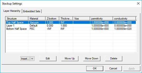
When you start a new project in EM.Picasso, there is always a default background structure that consists of a finite vacuum layer with a thickness of one project unit sandwiched between a vacuum top half-space and a PEC bottom half-space. Every time you open EM.Picasso or switched to it from EM.Cube's other modules, the Stack-up Settings Dialog opens up. This is where you define the entire background structure. Once you close this dialog, you can open it again by right-clicking the Layer Stack-up item in the Computational Domain section of the navigation tree and selecting Layer Stack-up Settings... from the contextual menu. Or alternatively, you can select the menu item Simulate > Computational Domain > Layer Stack-up Settings...
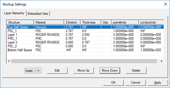
The Stack-up Settings dialog has two tabs: Layer Hierarchy and Embedded Sets. The Layer Hierarchy tab has a table that shows all the background layers in hierarchical order from the top half-space to the bottom half-space. It also lists the material composition of each layer, Z-coordinate of the bottom of each layer, its thickness (in project units) and material properties: permittivity (εr), permeability (μr), electric conductivity (σ) and magnetic conductivity (σm). There is also a column that lists the names of embedded object sets inside each substrate layer, if any.
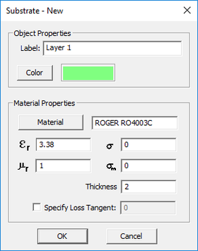
You can add new layers to your project's stack-up or delete its layers, or move layers up or down and thus change the layer hierarchy. To add a new background layer, click the arrow symbol on the Insert… button at the bottom of the dialog and select Substrate Layer from the button's dropdown list. A new dialog opens up where you can enter a label for the new layer and values for its material properties and thickness in project units. You can delete a layer by selecting its row in the table and clicking the Delete button. To move a layer up and down, click on its row to select and highlight it. Then click either the Move Up or Move Down buttons consecutively to move the selected layer to the desired location in the stack-up. Note that you cannot delete or move the top or bottom half-spaces. After creating a substrate layer, you can always edit its properties in the Layer Stack-up Settings dialog. Click on any layer's row in the table to select and highlight it and then click the Edit button. The substrate layer dialog opens up, where you can change the layer's label and assigned color as well as its constitutive parameters.
![]() Click here for a general discussion of Materials in EM.Cube.
Click here for a general discussion of Materials in EM.Cube.
![]() Click here to learn more about Using EM.Cube's Materials Database.
Click here to learn more about Using EM.Cube's Materials Database.
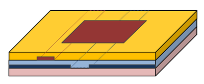
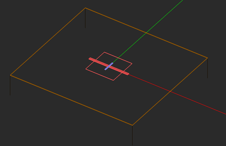
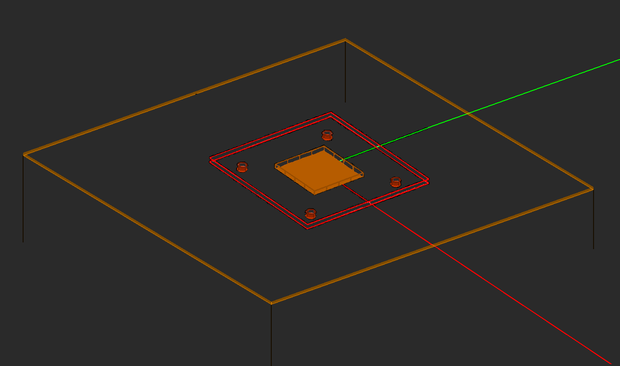
For better visualization of your planar structure, EM.Picasso displays a virtual domain in a default orange color to represent part of the infinite background structure. The size of this virtual domain is a quarter wavelength offset from the largest bounding box that encompasses all the finite objects in the project workspace. You can change the size of the virtual domain or its display color from the Domain Settings dialog, which you can access either by clicking the Computational Domain ![]() button of the Simulate Toolbar, or using the keyboard shortcut Ctrl+A. Keep in mind that the virtual domain is only for visualization purposes and its size does not affect the MoM simulation. The virtual domain also shows the substrate layers in translucent colors. If you assign different colors to your substrate layers, you have get a better visualization of multilayer virtual domain box surrounding your project structure.
button of the Simulate Toolbar, or using the keyboard shortcut Ctrl+A. Keep in mind that the virtual domain is only for visualization purposes and its size does not affect the MoM simulation. The virtual domain also shows the substrate layers in translucent colors. If you assign different colors to your substrate layers, you have get a better visualization of multilayer virtual domain box surrounding your project structure.
Planar Object & Trace Types
EM.Picasso groups objects by their trace type and their hierarchical location in the substrate layer stack-up. A trace is a group of finite-sized planar objects that have the same material properties, same color and same Z-coordinate. All the planar objects belonging to the same metal or slot trace group are located on the same horizontal boundary plane in the layer stack-up. All the embedded objects belonging to the same embedded set lie inside the same substrate layer and have same material composition.
EM.Picasso provides the following types of objects for building a planar layered structure (click on each type to learn more about it):
You can define two types of metallic traces in EM.Picasso: PEC Traces and Conductive Sheet Traces. PEC traces represent infinitesimally thin (zero thickness) planar metal objects that are deposited or metallized on or between substrate layers. PEC objects are modeled by surface electric currents. Conductive sheet traces, on the other hand, represent imperfect metals. They have a finite conductivity and a very small thickness expressed in project units. A surface impedance boundary condition is enforced on the surface of conductive sheet objects.
Slot Traces are used to model cut-out slots and apertures in PEC ground planes. Planar slot objects are always assumed to lie on an infinite horizontal PEC ground plane with zero thickness, which is not explicitly displayed in the project workspace and its presence is implied. They are modeled by surface magnetic currents. When a slot is excited, tangential electric fields are formed on the aperture, which can be modeled as finite magnetic surface currents confined to the area of the slot. In other words, instead of modeling the electric surface currents on an infinite PEC ground around the slot, one can alternatively model the finite-extent magnetic surface currents on a perfect magnetic conductor (PMC) trace. Slot (PMC) objects provide the electromagnetic coupling between the two sides of an infinite PEC ground plane.
Besides planar metal and slot traces, EM.Picasso allows you to insert prismatic embedded objects inside the substrate layers. The height of such embedded objects is always the same as the height of their host substrate layer. Two types of embedded object sets are available: PEC Via Sets and Embedded Dielectric Sets. PEC via sets are metallic objects such as shorting pins, interconnect vias, plated-through holes, etc. all located and grouped together inside the same substrate layer. The embedded via objects are modeled as vertical volume conduction currents. Embedded dielectric sets are prismatic dielectric objects inserted inside a substrate layer. You can define a finite permittivity and conductivity for such objects. The embedded dielectric objects are modeled as vertical volume polarization currents.
![]() Click here to learn more about Defining Materials in EM.Cube.
Click here to learn more about Defining Materials in EM.Cube.
| |
The height of an embedded object is always identical to the thickness of its host substrate layer. |
Defining Traces & Embedded Object Sets
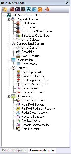
When you start a new project in EM.Picasso, the project workspace looks empty, and there are no finite objects in it. However, a default background structure is always present. Finite objects are defined as part of traces or embedded sets. Once defined, you can see a list of project objects in the Physical Structure section of the navigation tree. Traces and object sets can be defined either from Layer Stack-up Settings dialog or from the navigation tree. In the Layer Stack-up Settings dialog, you can add a new trace to the stack-up by clicking the arrow symbol on the Insert button of the dialog. You have to choose from Metal (PEC), Slot (PMC) or Conductive Sheet options. A respective dialog opens up, where you can enter a label and assign a color. Once a new trace is defined, it is added, by default, to the top of the stack-up table underneath the top half-space. From here, you can move the trace down to the desired location on the layer hierarchy. Every time you define a new trace, it is also added under the respective category in the navigation tree. Alternatively, you can define a new trace from the navigation tree by right-clicking on one of the trace type names and selecting Insert New PEC Trace...or Insert New PMC Trace...or Insert New Conductive Sheet Trace... A respective dialog opens up for setting the trace properties. Once you close this dialog, it takes you directly to the Layer Stack-up Settings dialog so that you can set the right position of the trace on the stack-up.
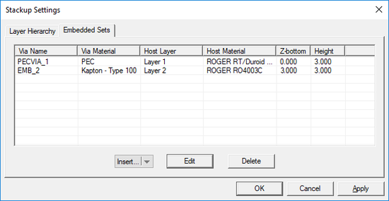
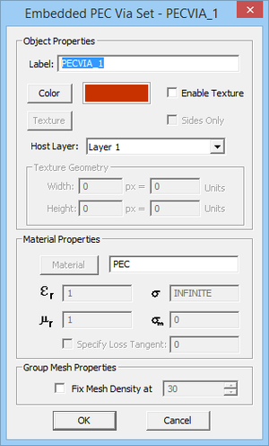
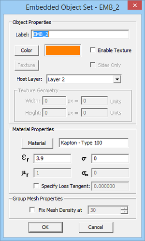
Embedded object sets represent short material insertions inside substrate layers. They can be metal or dielectric. Metallic embedded objects can be used to model vias, plated-through holes, shorting pins and interconnects. These are called PEC via sets. Embedded dielectric objects can be used to model air voids, thin films and material inserts in metamaterial structures. Embedded objects can be defined either from the Layer Stack-up Settings dialog or directly from the navigation tree. Open the "Embedded Sets" tab of the stack-up dialog. This tab has a table that lists all the embedded object sets along with their material type, the host substrate layer, the host material and their height. To add a new object set, click the arrow symbol on the Insert button of the dialog and select one of the two options, PEC Via Set or Embedded Dielectric Set, from the dropdown list. This opens up a new dialog where first you have to set the host layer of the new object set. A dropdown list labeled "Host Layer" gives a list of all the available finite substrate layers. You can also set the properties of the embedded object set, including its label, color and material properties. Keep in mind that you cannot control the height of embedded objects. Moreover, you cannot assign material properties to PEC via sets, while you can set values for the Permittivity(εr) and Electric Conductivity(σ) of embedded dielectric sets. Vacuum is the default material choice. To define an embedded set from the navigation tree, right-click on the Embedded Object Sets item in the Physical Structure section of the navigation tree and select either Insert New PEC Via Set... or Insert New Embedded Dielectric Set... The respective New Embedded Object Set dialog opens up, where you can set the properties of the new object set. As soon as you close this dialog, it takes you to the Layer Stack-up Settings dialog, where you can verify the location of the new object set on the layer hierarchy.
![]() Click here to learn more about Defining Materials in EM.Cube.
Click here to learn more about Defining Materials in EM.Cube.
Drawing Planar Objects on Horizontal Work Planes
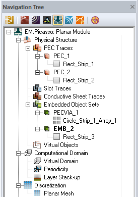
As soon as you start drawing geometrical objects in the project workspace, the Physical Structure section of the navigation tree gets populated. The names of traces are added under their respective trace type category, and the names of objects appear under their respective trace group. At any time, one and only one trace is active in the project workspace. The name of the active trace in the navigation tree is always displayed in bold letters. An active trace is where all the new objects you draw belong to. By default, the last defined trace or embedded object set is active. You can immediately start drawing new objects on the active trace. You can also set any trace or object set group active at any time by right-clicking on its name on the navigation tree and selecting Activate from the contextual menu.
![]() Click here to learn more about Defining a New Trace Group.
Click here to learn more about Defining a New Trace Group.
![]() Click here to learn more about Moving Objects among Trace Groups.
Click here to learn more about Moving Objects among Trace Groups.
EM.Picasso has a special feature that makes construction of planar structures very convenient and straightforward. The horizontal Z-plane of the active trace or object set group is always set as the active work plane of the project workspace. That means all new objects are drawn at the Z-coordinate of the currently active trace. As you change the active trace group or add a new one, the active work plane changes accordingly.
| |
In EM.Picasso, you cannot modify the Z-coordinate of an object as it is set and controlled by its host trace. |
EM.Picasso does not allow you to draw 3D or solid CAD objects. The solid object buttons in the Object Toolbar are disabled to prevent you from doing so. In order to create vias and embedded object, you simply have to draw their cross section geometry using planar surface CAD objects. EM.Picasso extrudes and extends these planar objects across their host layer automatically and displays them as 3D wireframe, prismatic objects. The automatic extrusion of embedded objects happens after mesh generation and before every planar MoM simulation. You can enforce this extrusion manually by right-clicking the Layer Stack-up item in the "Computational Domain" section of the navigation tree and selecting Update Planar Structure from the contextual menu.
| |
In EM.Picasso, you can only draw horizontal planar surface CAD objects. |
EM.Picasso's Special Rules
- PEC ground planes at the top or bottom of a planar structure are regarded and modeled as PEC top or bottom half-spaces, respectively.
- A PEC ground plane placed in the middle of a substrate stack-up requires at least one slot object to provide electromagnetic coupling between its top and bottom sides. In this case, a slot trace is rather introduced at the given Z-plane, which also implies the presence of an infinite PEC ground.
- Metallic and slot traces cannot coexist on the same Z-plane. However, you can stack up multiple PEC and conductive sheet traces at the same Z-coordinate. Similarly, multiple slot traces can be placed at the same Z-coordinate.
- Metallic and slot traces are strictly defined at the interface planes between substrate layers. To define a suspended metallic trace inside a dielectric layer (as in the case of the center conductor of a stripline), you must split the dielectric layer into two thinner substrate layers and place your PEC trace at the interface between them.
- EM.Picasso's simulation engine is based on a 2.5-D MoM formulation. Only vertical volume currents and no circumferential components are allowed on embedded objects. The 2.5-D assumption holds very well in two cases: (a) when embedded objects are very thin with a very small cross section (with lateral dimensions less than 2-5% of the material wavelength) or (b) when embedded objects are very short and sandwiched between two closely spaced PEC traces or grounds from the top and bottom.
Discretizing the Planar Structure
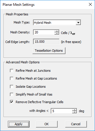
The method of moments (MoM) discretizes all the finite-sized objects of a planar structure (excluding the background structure) into a set of elementary cells. Both the quality and resolution of the generated mesh greatly affect the accuracy of the MoM numerical solution. The mesh density gives a measure of the number of cells per effective wavelength that are placed in various regions of your planar structure. The higher the mesh density, the more cells are created on the finite-sized geometrical objects. As a rule of thumb, a mesh density of about 20-30 cells per effective wavelength usually yields satisfactory results. But for structures with lots of fine geometrical details or for highly resonant structures, higher mesh densities may be required. The particular output data that you seek in a simulation also influence your choice of mesh resolution. For example, far field characteristics like radiation patterns are less sensitive to the mesh density than field distributions on structures with a highly irregular shapes and boundaries.
EM.Picasso provides two types of mesh for a planar structure: a pure triangular surface mesh and a hybrid triangular-rectangular surface mesh. In both case, EM.Picasso attempts to create a highly regular mesh, in which most of the cells have almost equal areas. For planar structures with regular, mostly rectangular shapes, the hybrid mesh generator usually leads to faster computation times.
![]() Click here to learn more about Working with Mesh Generator .
Click here to learn more about Working with Mesh Generator .
![]() Click here to learn more about EM.Picasso's Triangular Surface Mesh Generator.
Click here to learn more about EM.Picasso's Triangular Surface Mesh Generator.
![]() Click here to learn more about EM.Picasso's Hybrid Planar Mesh Generator.
Click here to learn more about EM.Picasso's Hybrid Planar Mesh Generator.
![]() Click here to learn more about General Rules of Planar Hybrid Mesh Generator.
Click here to learn more about General Rules of Planar Hybrid Mesh Generator.
![]() Click here to learn more about Refining the Planar Mesh Locally.
Click here to learn more about Refining the Planar Mesh Locally.
Excitation Sources
Your planar structure must be excited by some sort of signal source that induces electric surface currents on metal parts, magnetic surface currents on slot traces, and conduction or polarization volume currents on vertical vias and embedded objects. The excitation source you choose depends on the observables you seek in your project. EM.Picasso provides the following source types for exciting planar structures (click on each type to learn more about it):
- Gap Sources
- Probe Sources
- De-embedded Sources
- Short Dipole Sources
- Plane Wave Sources
- Huygens Sources
For antennas and planar circuits, where you typically define one or more ports, you usually use lumped sources. EM.Picasso provides three types of lumped sources: gap source, probe source and de-embedded source. A lumped source is indeed a gap discontinuity that is placed on the path of an electric or magnetic current flow, where a voltage or current source is connected to inject a signal. Gap sources are placed across metal or slot traces. A rectangle strip object on a PEC or conductive sheet trace acts like a strip transmission line that carries electric currents along its length (local X direction). The characteristic impedance of the line is a function of its width (local Y direction). A gap source placed on a narrow metal strip creates a uniform electric field across the gap and pumps electric current into the line. A rectangle strip object on a slot trace acts like a slot transmission line on an infinite PEC ground plane that carries a magnetic current along its length (local X direction). The characteristic impedance of the slot line is a function of its width (local Y direction). A gap source placed on a narrow slot represents an ideal current source. A slot gap acts like an ideal current filament, which creates electric fields across the slot, equivalent to a magnetic current flowing into the slot line. Probe sources are placed across vertical PEC vias. A de-embedded source is a special type of gap source that is placed near the open end of an elongated metal or slot trace to create a standing wave pattern, from which the scattering parameters can be calculated accurately.
| |
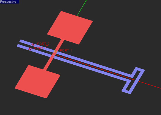
You can realize a coplanar waveguide (CPW) in EM.Picasso using two parallel slot lines with two aligned, collocated gap sources. |
![]() Click here to learn more about Using Source Arrays for Modeling Antenna Arrays.
Click here to learn more about Using Source Arrays for Modeling Antenna Arrays.
A short dipole provides another way of exciting a planar structure in EM.Picasso. A short dipole source acts like an infinitesimally small ideal current source. You can also use an incident plane wave to excite your planar structure in EM.Picasso. In particular, you need a plane wave source to compute the radar cross section of a planar structure. The direction of incidence is defined by the θ and φ angles of the unit propagation vector in the spherical coordinate system. The default values of the incidence angles are θ = 180° and φ = 0° corresponding to a normally incident plane wave propagating along the -Z direction with a +X-polarized E-vector. Huygens sources are virtual equivalent sources that capture the radiated electric and magnetic fields from another structure that was previously analyzed in another EM.Cube computational module.
Modeling Lumped Elements in EM.Picasso
Lumped elements are components, devices, or circuits whose overall dimensions are very small compared to the wavelength. As a result, they are considered to be dimensionless compared to the dimensions of a mesh cell. In fact, a lumped element is equivalent to an infinitesimally narrow gap that is placed in the path of current flow, across which the device's governing equations are enforced. Using Kirkhoff's laws, these device equations normally establish a relationship between the currents and voltages across the device or circuit. Crossing the bridge to Maxwell's domain, the device equations must now be cast into a from o boundary conditions that relate the electric and magnetic currents and fields. EM.Picasso allows you to define passive circuit elements: Resistors (R), Capacitors (C), Inductors (L), and series and parallel combinations of them.
![]() Click here to learn more about Defining Lumped Elements.
Click here to learn more about Defining Lumped Elements.
![]() Click here for a general discussion of Linear Passive Devices.
Click here for a general discussion of Linear Passive Devices.
Defining Independent & Coupled Ports
Ports are used in a planar structure to order and index the sources for calculation of circuit parameters such as scattering (S), impedance (Z) and admittance (Y) parameters. In EM.Picasso, you can use one or more of the following types of sources to define ports:
- Gap Sources
- Probe Sources
- Active Lumped Elements
- De-Embedded Sources
Ports are defined in the Observables section of the navigation tree. You can define any number of ports equal to or less than the total number of sources in your project. If you have N sources in your planar structure, then N default ports are defined, with one port assigned to each source according to their order on the navigation tree. Note that your project can have mixed gap and probes sources as well as active lumped element sources on PEC and slot traces or vias. You can also couple ports together to define coupled transmission lines such as coupled strips (CPS) or coplanar waveguides (CPW).
![]() Click here to learn more about the Port Definition Observable.
Click here to learn more about the Port Definition Observable.
![]() Click here to learn more about Modeling Coupled Ports.
Click here to learn more about Modeling Coupled Ports.
Running Planar MoM Simulations
EM.Picasso's Simulation Modes
EM.Picasso offers five Planar MoM simulation modes (click on each type to learn more about it):
- Single-Frequency Analysis
- Frequency Sweep: including uniform and adaptive frequency sweeps
- Parametric Sweep
- Optimization
- HDMR Sweep
You can set the simulation mode from EM.Picasso's "Simulation Run Dialog". A single-frequency analysis is a single-run simulation. All the other simulation modes in the above list are considered multi-run simulations. If you run a simulation without having defined any observables, no data will be generated at the end of the simulation. In multi-run simulation modes, certain parameters are varied and a collection of simulation data files are generated. At the end of a sweep simulation, you can graph the simulation results in EM.Grid or you can animate the 3D simulation data from the navigation tree.
Running a Single-Frequency Planar MoM Analysis
A single-frequency analysis is the simplest type of EM.Picasso simulation and involves the following steps:
- Set the units of your project and the frequency of operation. Note that the default project unit is millimeter.
- Define you background structure and its layer properties and trace types.
- Construct your planar structure using CubeCAD's drawing tools to create all the finite-sized metal and slot trace objects and possibly embedded metal or dielectric objects that are interspersed among the substrate layers.
- Define an excitation source and observables for your project.
- Examine the planar mesh, verify its integrity and change the mesh density if necessary.
- Run the Planar MoM simulation engine.
- Visualize the output simulation data.
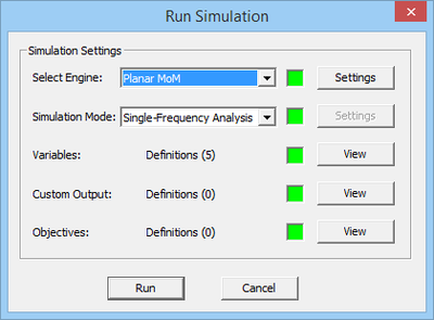
To run a planar MoM analysis of your project structure, open the Run Simulation Dialog by clicking the Run ![]() button on the Simulate Toolbar or select Menu > Simulate > Run or use the keyboard shortcut Ctrl+R. The Single-Frequency Analysis option of the Simulation Mode dropdown list is selected by default. Once you click the Run button, the simulation starts. A new window called the "Output Window" opens up that reports the different stages of simulation and the percentage of the tasks completed at any time. After the simulation is successfully completed, a message pops up and reports the end of simulation. In certain cases like calculating scattering parameters of a circuit or reflection / transmission characteristics of a periodic surface, some results are also reported in the output window.
button on the Simulate Toolbar or select Menu > Simulate > Run or use the keyboard shortcut Ctrl+R. The Single-Frequency Analysis option of the Simulation Mode dropdown list is selected by default. Once you click the Run button, the simulation starts. A new window called the "Output Window" opens up that reports the different stages of simulation and the percentage of the tasks completed at any time. After the simulation is successfully completed, a message pops up and reports the end of simulation. In certain cases like calculating scattering parameters of a circuit or reflection / transmission characteristics of a periodic surface, some results are also reported in the output window.
Setting Numerical Parameters
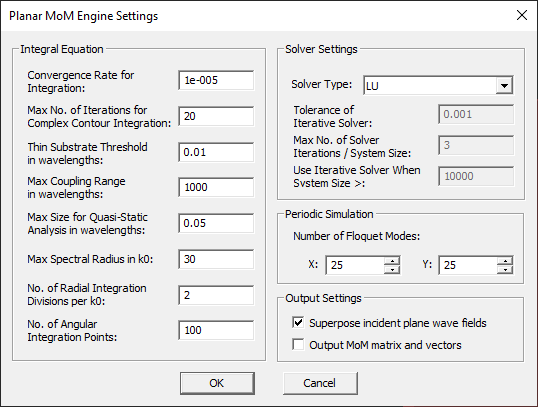
A planar MoM simulation involves a number of numerical parameters that take preset default values unless you change them. You can access these parameters and change their values by clicking the Settings button next to the Select Engine dropdown list in the Planar Module's Simulation Run dialog. In most cases, you do not need to open this dialog and you can leave all the default numerical parameter values intact. However, it is useful to familiarize yourself with these parameters, as they may affect the accuracy of your numerical results.
The Planar MoM Engine Settings Dialog is organized in a number of sections. Here we describe some of the numerical parameters. The "Matrix Fill" section of the dialog deals with the operations involving the dyadic Green's functions. You can set a value for the Convergence Rate for Integration, which is 1E-5 by default. This is used for the convergence test of all the infinite integrals in the calculation of the Hankel transform of spectral-domain dyadic Green's functions. When the substrate is lossy, the surface wave poles are captured in the complex integration plane using contour deformation. You can change the maximum number of iterations involved in this deformed contour integration, whose default value is 20. When the substrate is very thin with respect to the wavelength, the dyadic Green's functions exhibit numerical instability. Additional singularity extraction measures are taken to avoid numerical instability but at the expense of increased computation time. By default, a thin substrate layer is defined to a have a thickness less than 0.01λeff, where λeff is the effective wavelength. You can modify the definition of "Thin Substrate" by entering a value for Thin Substrate Threshold different than the default 0.01. The parameter Max Coupling Range determines the distance threshold in wavelength between the observation and source points after which the Green's interactions are neglected. This distance by default is set to 1,000 wavelengths. For electrically small structures, the phase variation across the structure may be negligible. In such cases, a fast quasi-static analysis can be carried out. You can set this threshold in wavelengths in the box labeled Max Dimensions for Quasi-Static Analysis.
In the "Spectral Domain Integration" section of the dialog, you can set a value to Max Spectral Radius in k0, which has a default value of 30. This means that the infinite spectral-domain integrals in the spectral variable kρ are pre-calculated and tabulated up to a limit of 30k0, where k0 is the free space propagation constant. These integrals may converge much faster based on the specified Convergence Rate for Integration described earlier. However, in certain cases involving highly oscillatory integrands, much larger integration limits like 100k0 might be needed to warrant adequate convergence. For spectral-domain integration along the real kρ axis, the interval [0, Nk0] is subdivided into a large number of sub-intervals, within each an 8-point Gauss-Legendre quadrature is applied. The next parameter, No. Radial Integration Divisions per k0, determines how small these intervals should be. By default, 2 divisions are used for the interval [0, k0]. In other words, the length of each integration sub-interval is k0/2. You can increase the resolution of integration by increasing this value above 2. Finally, instead of 2D Cartesian integration in the spectral domain, a polar integration is performed. You can set the No. of Angular Integration Points, which has a default value of 100.
EM.Picasso provides a large selection of linear system solvers including both direct and iterative methods. EM.Picasso, by default, provides a "Automatic" solver option that picks the best method based on the settings and size of the numerical problem. For linear systems with a size less than N = 3,000, the LU solver is used. For larger systems, BiCG is used when dealing with symmetric matrices, and GMRES is used for asymmetric matrices. You can instruct EM.Cube to write the MoM matrix and excitation and solution vectors into output data files for your examination. To do so, check the box labeled "Output MoM Matrix and Vectors" in the Matrix Fill section of the Planar MoM Engine Settings dialog. These are written into three files called mom.dat1, exc.dat1 and soln.dat1, respectively.
Working with EM.Picasso Simulation Data
Depending on the source type and the types of observables defined in a project, a number of output data are generated at the end of a planar MoM simulation. Some of these data are 2D by nature and some are 3D. The output simulation data generated by EM.Picasso can be categorized into the following groups (click on each type to learn more about it):
- Current Distributions: Electric and magnetic current amplitude and phase on all metal and slot traces and embedded objects
- Port Characteristics: S, Z and Y Parameters and Voltage Standing Wave Ratio (VSWR)
- Near-Field Distributions: Electric and magnetic field amplitude and phase on specified planes and their central axes
- Radiation Characteristics: Radiation Patterns, Directivity, Total Radiated Power, Axial Ratio, Main Beam Theta and Phi, Radiation Efficiency, Half Power Beam Width (HPBW), Maximum Side Lobe Level (SLL), First Null Level (FNL), Front-to-Back Ratio (FBR), etc.
- Radar Cross Section: Bi-static and Mono-static Radar Cross Section (RCS)
- Periodic Characteristics: Reflection and Transmission Coefficients
If your planar structure is excited by gap sources or probe sources or de-embedded sources, and one or more ports have been defined, the planar MoM engine calculates the scattering, impedance and admittance (S/Z/Y) parameters of the designated ports. The scattering parameters are defined based on the port impedances specified in the project's Port Definition dialog. If more than one port has been defined in the project, the S/Z/Y matrices of the multiport network are calculated.
![]() Click here to learn more about Computing and Graphing Port Characteristics.
Click here to learn more about Computing and Graphing Port Characteristics.
![]() Click here to learn more about Rational Interpolation of Scattering Parameters.
Click here to learn more about Rational Interpolation of Scattering Parameters.
Electric and magnetic currents are the fundamental output data of a planar MoM simulation. After the numerical solution of the MoM linear system, they are found using the solution vector [I] and the definitions of the electric and magnetic vectorial basis functions:
- [math] \mathbf{[X]}_{N\times 1} = \begin{bmatrix} I^{(J)} \\ \\ V^{(M)} \end{bmatrix} \quad \Rightarrow \quad \begin{cases} \mathbf{J(r)} = \sum_{n=1}^N I_n^{(J)} \mathbf{f_n^{(J)} (r)} \\ \\ \mathbf{M(r)} = \sum_{k=1}^K V_k^{(M)} \mathbf{f_k^{(M)} (r)} \end{cases} [/math]
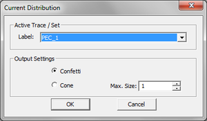
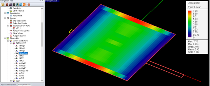
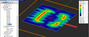
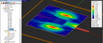
Note that currents are complex vector quantities. Each electric or magnetic current has three X, Y and Z components, and each complex component has a magnitude and phase. You can visualize the surface electric currents on metal (PEC) and conductive sheet traces, surface magnetic currents on slot (PMC) traces and vertical volume currents on the PEV vias and embedded dielectric objects. 3D color-coded intensity plots of electric and magnetic current distributions are visualized in the project workspace, superimposed on the surface of physical objects. In order to view the current distributions, you must first define them as observables before running the planar MoM simulation. At the top of the Current Distribution dialog and in the section titled Active Trace / Set, you can select a trace or embedded object set where you want to observe the current distribution.
| |
You have to define a separate current distribution observable for each individual trace or embedded object set. |
![]() Click here to learn more about Visualizing 3D Current Distribution Maps.
Click here to learn more about Visualizing 3D Current Distribution Maps.

![]() Click here to learn more about Defining a Field Sensor Observable.
Click here to learn more about Defining a Field Sensor Observable.
![]() Click here to learn more about Visualizing 3D Near Field Maps.
Click here to learn more about Visualizing 3D Near Field Maps.
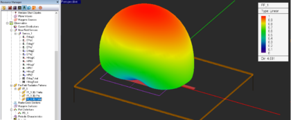
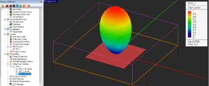
Even though EM.Picasso's MoM engine does not need a radiation box, you still have to define a "Far Field" observable for radiation pattern calculation. This is because far field calculations take time and you have to instruct EM.Cube to perform these calculations. Once a planar MoM simulation is finished, three far field items are added under the Far Field item in the Navigation Tree. These are the far field component in θ direction, the far field component in φ direction and the "Total" far field. The 2D radiation pattern graphs can be plotted from the Data Manager. A total of eight 2D radiation pattern graphs are available: 4 polar and 4 Cartesian graphs for the XY, YZ, ZX and user defined plane cuts.
![]() Click here to learn more about Far Field Observables.
Click here to learn more about Far Field Observables.
![]() Click here to learn more about the theory of Using Array Factors to Model Antenna Arrays .
Click here to learn more about the theory of Using Array Factors to Model Antenna Arrays .
![]() Click here to learn more about Visualizing 3D Radiation Patterns.
Click here to learn more about Visualizing 3D Radiation Patterns.
![]() Click here to learn more about Plotting 2D Radiation Graphs.
Click here to learn more about Plotting 2D Radiation Graphs.
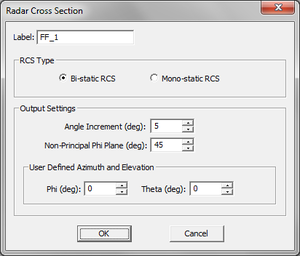
When a planar structure is excited by a plane wave source, the calculated far field data indeed represent the scattered fields of that planar structure. EM.Picasso can also calculate the radar cross section (RCS) of a planar target. Note that in this case the RCS is defined for a finite-sized target in the presence of an infinite background structure. The scattered θ and φ components of the far-zone electric field are indeed what you see in the 3D far field visualization of radiation (scattering) patterns. Instead of radiation or scattering patterns, you can instruct EM.Picasso to plot 3D visualizations of σθ, σφ and the total RCS.
![]() Click here to learn more about Computing Radar Cross Section.
Click here to learn more about Computing Radar Cross Section.
![]() Click here to learn more about Plotting 2D RCS Graphs.
Click here to learn more about Plotting 2D RCS Graphs.

