EM.Illumina
EM.Illumina is a 3D electromagnetic simulator for modeling large free-space structures. It features a high frequency asymptotic solver based on Physical Optics (PO) for simulation of electromagnetic scattering from large metallic structures and impedance surfaces.
EM.Illumina provides a computationally efficient alternative for extremely large structures when a full-wave solution becomes prohibitively expensive. Based on a high frequency asymptotic physical optics formulation, it assumes that an incident source generates currents on a metallic structure, which in turn reradiate into the free space. A challenging step in establishing the PO currents is the determination of the lit and shadowed points on complex scatterer geometries. Ray tracing from each source to the points on the scatterers to determine whether they are lit or shadowed is a time consuming task. To avoid this difficulty, EM.Illumina's simulator uses a novel Iterative Physical Optics (IPO) formulation, which automatically accounts for multiple shadowing effects.The IPO technique can effectively capture dominant, near-field, multiple scattering effects from electrically large targets.
EM.Illumina's simulator is seamlessly interfaced with EM.CUBE's other simulattion engines. This module is the ideal place to define Huygens sources. These are based on Huygens surface data that are generated using a full-wave simulator like EM.Picasso, EM.Tempo or EM.Libera.
Contents
- 1 Methods Of Physical Optics
- 2 Physical Structure & Its Discretization
- 3 Excitation Sources
- 4 Running PO Simulations
- 4.1 Running A Basic PO Analysis
- 4.2 Setting The Numerical Parameters
- 4.3 Visualizing Current Distributions
- 4.4 Near Field Visualization
- 4.5 Visualizing 3D Radiation Patterns
- 4.6 Radar Cross Section
- 4.7 Customizing 3D Plots
- 4.8 2D Radiation Pattern & RCS Graphs
- 4.9 PO Sweep Simulations
- 4.10 Animation Of PO Data
Methods Of Physical Optics
Physical Optics As An Asymptotic Technique
Many larger-scale electromagnetic problems deal with the modeling of radar scattering from large metallic structures (targets like aircraft or vehicles) or the radiation of antennas in the presence of large scatterer platforms. Although a full-wave analysis of such open-boundary computational problems using the method of moments (MoM) is conceptually feasible, it may not be practical due to the enormous memory requirements for storage of the resulting moment matrices. To solve this class of problems, you may instead pursue asymptotic electromagnetic analysis methods.
Asymptotic methods are usually valid at high frequencies as [math]k_0 R = 2\pi R/\lambda_0 \gt\gt 1[/math], where R is the distance between the source and observation points, k0 is the free-space propagation constant and λ0 is the free-space wavelength. Under such conditions, electromagnetic fields and waves start to behave more like optical fields and waves. Asymptotic methods are typically inspired by optical analysis. Two important examples of asymptotic methods are the Shoot-and-Bounce-Rays (SBR) method and Physical Optics (PO). The SBR method, which is featured in EM.Cube's Propagation Module, is a ray tracing method based on Geometrical Optics (GO). An SBR analysis starts by shooting a number of ray tubes (or beams) off a source. It then traces all the rays as they propagate in the scene or bounce off the surface of obstructing scatterers. The uniform theory of diffraction (UTD) is used to model the diffraction of rays at the edges of the structure.
In the Physical Optics (PO) method, a scatterer surface is illuminated by an incident source, and it is modeled by equivalent electric and magnetic surface currents. This concept is based on the fundamental equivalence theorem of electromagnetics and the Huygens principle. The electric surface currents are denoted by J(r) and the magnetic surface currents are denoted by M(r), where r is the position vector. According to the Huygens principle, the equivalent electric and magnetic surface currents are derived from the tangential components of magnetic and electric fields on a given surface, respectively. This will be discussed in more detail in the next sections. In a classic PO analysis which involves only perfect electric conductors, only electric surface currents, related to the tangential magnetic fields, are considered.
Conventional Physical Optics (GO-PO)
The following analysis assumes a general impedance surface. To treat an object with an arbitrary geometry using PO, the object is first decomposed into many small elementary patches or cells, which have a simple geometry such as a rectangle or triangle. Then, using the tangent plane approximation, the electric and magnetic surface currents, J(r) and M(r), on the lit region of the scatterer are approximated by:
- [math] \mathbf{J(r)} = (1+\alpha) \mathbf{\hat{n} \times H(r)} [/math]
- [math] \mathbf{M(r)} = -(1-\alpha) \mathbf{\hat{n} \times E(r)} [/math]
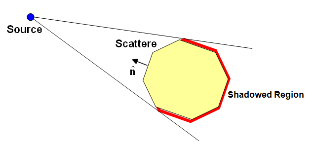
where E(r) and H(r) are the incident electric and magnetic fields on the object and n is the local outward normal unit vector as shown in the figure below. a is a parameter related to the impedance Z of the surface (expressed in Ohms), which is defined in the following way:
- [math] \alpha = \frac{1-Z/\eta_0}{1+Z/\eta_0} [/math]
where [math]\eta_0 = 120\pi \; \Omega[/math] is the intrinsic impedance of the free space. Then, the electric and magnetic currents reduce to:
- [math] \mathbf{J(r)} = \frac{2\eta_0}{\eta_0 + Z} \mathbf{\hat{n} \times H(r)} [/math]
- [math] \mathbf{M(r)} = - \frac{2Z}{\eta_0 + Z} \mathbf{\hat{n} \times E(r)} [/math]
Two limiting cases of an impedance surface are perfect electric conductor (PEC) and perfect magnetic conductor (PMC) surface. For a PEC surface, Z = 0, α = 1, and one can write:
- [math] \mathbf{J(r)} = 2 \mathbf{\hat{n} \times H(r)} [/math]
- [math] \mathbf{M(r)} = 0 [/math]
while for a PMC surface, Z = 8, α = -1, and one can write:
- [math] \mathbf{J(r)} = 0 [/math]
- [math] \mathbf{M(r)} = -2 \mathbf{\hat{n} \times E(r)} [/math]
Another special case is a Huygens surface with equivalent electric and magnetic surface currents. In that case, Z = η0, α = 0, and one can write:
- [math] \mathbf{J(r) = \hat{n} \times H(r)} [/math]
- [math] \mathbf{M(r) = -\hat{n} \times E(r)} [/math]
Figure 1: A diagram showing a scatterer lit by a source.
A major difficulty encountered in determining the PO currents of the scatterer is identification of lit and shadowed facets. Determination of lit and shadowed regions for simple, stand-alone, convex objects is rather simple. Denoting the incidence direction from a source to a point on the scatterer by the unit vector k, the point is considered lit if n.k< 0, and shadowed if n.k> 0. These conditions, however, are only valid if there is a direct line of sight (LOS) between the source and the centroid of the cell under consideration. They cannot predict if there are any obstructing objects in the path of the incident beam or ray. For simple convex objects, a Geometrical Optics (GO) approach can be used to finds the optical LOS lines and determine the lit and shadowed areas on the object. The conventional PO can then be used to find the electric and magnetic surface currents.
Calculating Near & Far Fields In PO
Once the electric and magnetic surface currents are determined in the lit regions of the scatterer(s), they act as secondary sources and radiate into the free space. These secondary fields are the scattered fields that are superposed with the primary incident fields. The near fields at every point r in space are calculated from:
- [math] \mathbf{ E(r) = E^{inc}(r) } + \iint_{S_J} \mathbf{ \overline{\overline{G}}_{EJ}(r|r') \cdot J(r') } ds' + \iint_{S_M} \mathbf{ \overline{\overline{G}}_{EM}(r|r') \cdot M(r') } ds' [/math]
- [math] \mathbf{ H(r) = H^{inc}(r) } + \iint_{S_J} \mathbf{ \overline{\overline{G}}_{HJ}(r|r') \cdot J(r') } ds' + \iint_{S_M} \mathbf{ \overline{\overline{G}}_{HM}(r|r') \cdot M(r') } ds' [/math]
where GEJ, GEM, GHJ, GHM are the dyadic Green's functions of electric and magnetic fields due to electric and magnetic currents, respectively. In EM.Cube's PO Module, the background structure is the free space. Therefore, all these dyadic Green's functions reduce to the simple free-space Green's function of the form [math]\exp(-jk_0r)/(4\pi r)[/math] and the near fields reduce to:
- [math] \begin{align} \mathbf{ E(r) = E^{inc}(r) } & - jk_0 Z_0 \iint_{S_J} \left\{ \left[ 1 - \frac{j}{k_0 R} - \frac{1}{(k_0 R)^2} \right] \mathbf{J(r')} - \left[ 1 - \frac{3j}{k_0 R} - \frac{3}{(k_0 R)^2} \right] \mathbf{ (\hat{R} \cdot J(r')) \hat{R} } \right\} \frac{e^{-jk_0 R}}{4\pi R} ds' \\ & + jk_0 \iint_{S_M} \left[ 1-\frac{j}{k_0 R} \right] \mathbf{ (\hat{R} \times M(r')) } \frac{e^{-jk_0 R}}{4\pi R} ds' \end{align} [/math]
- [math] \begin{align} \mathbf{ H(r) = H^{inc}(r) } & - jk_0 Y_0 \iint_{S_M} \left\{ \left[ 1 - \frac{j}{k_0 R} - \frac{1}{(k_0 R)^2} \right] \mathbf{M(r')} - \left[ 1 - \frac{3j}{k_0 R} - \frac{3}{(k_0 R)^2} \right] \mathbf{ (\hat{R} \cdot M(r')) \hat{R} } \right\} \frac{e^{-jk_0 R}}{4\pi R} ds' \\ & - jk_0 \iint_{S_J} \left[ 1-\frac{j}{k_0 R} \right] \mathbf{ (\hat{R} \times J(r')) } \frac{e^{-jk_0 R}}{4\pi R} ds' \end{align} [/math]
where [math] R=|r-r'| \text{, } k_0 = \tfrac{2\pi}{\lambda_0} \text{ and } Z_0 = 1/Y_0 = \eta_0 [/math].
When k0r >> 1, i.e. in the far-zone field of the scatterer, one can use the asymptotic form of the Green's functions and evaluate the radiation integrals using the stationary phase method to obtain far-field expressions for the electric and magnetic fields as follows:
- [math] \mathbf{E^{ff}(r)} = \frac{jk_0 e^{-jk_0 r}}{4\pi r} \left\{ Z_0 \mathbf{ \hat{r} \times \hat{r} } \times \iint_{S_J} \mathbf{J(r')} e^{-jk_0 \mathbf{\hat{r}\cdot r'}} ds' + \mathbf{\hat{r}} \times \iint_{S_M} \mathbf{M(r')} e^{-jk_0 \mathbf{ \hat{r} \cdot r' } } ds' \right\} [/math]
- [math] \mathbf{H^{ff}(r)} = \frac{1}{Z_0} \mathbf{\hat{r} \times E^{ff}(r)} [/math]
Iterative Physical Optics (IPO)
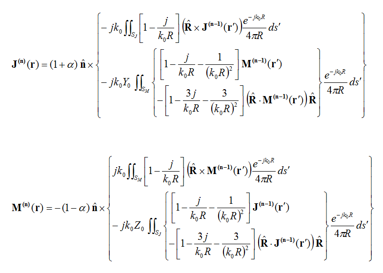
The induced electric and magnetic surface currents on each point of the scatterer object can be calculated from the Magnetic and Electric Field Integral Equations (MFIE & EFIE):
- [math] \mathbf{J(r)} = (1+\alpha)\mathbf{\hat{n}} \times \left\lbrace \begin{align} & \mathbf{ H^{inc}(r) } - jk_0 \iint_{S_J} \left( 1 - \frac{j}{k_0 R} \right) (\mathbf{ \hat{R} \times J(r') }) \frac{e^{-jk_0 R}}{4\pi R} \,ds' \\ & -j k_0 Y_0 \iint_{S_M} \left[ \left( 1 - \frac{j}{k_0 R} - \frac{1}{(k_0 R)^2} \right) \mathbf{M(r')} - \left( 1-\frac{3j}{k_0 R}-\frac{3}{(k_0 R)^2} \right) \mathbf{ (\hat{R} \cdot M(r')) \hat{R} } \right] \frac{e^{-jk_0 R}}{4\pi R} \,ds' \end{align} \right\rbrace [/math]
- [math] \mathbf{M(r)} = -(1-\alpha)\mathbf{\hat{n}} \times \left\lbrace \begin{align} & \mathbf{ E^{inc}(r) } + jk_0 \iint_{S_M} \left( 1 - \frac{j}{k_0 R} \right) (\mathbf{ \hat{R} \times M(r') }) \frac{e^{-jk_0 R}}{4\pi R} \,ds' \\ & -j k_0 Z_0 \iint_{S_J} \left[ \left( 1 - \frac{j}{k_0 R} - \frac{1}{(k_0 R)^2} \right) \mathbf{J(r')} - \left( 1-\frac{3j}{k_0 R}-\frac{3}{(k_0 R)^2} \right) \mathbf{ (\hat{R} \cdot J(r')) \hat{R} } \right] \frac{e^{-jk_0 R}}{4\pi R} \,ds' \end{align} \right\rbrace [/math]
where R =r - r', R = |R|, and
- [math]\mathbf{ \hat{R} = \frac{R}{|R|} = \frac{r-r'}{|r-r'|} }[/math]
The shadowing phenomenon can indeed be attributed to near-field interaction of surface currents. The current on the lit region produces a scattered field in the forward direction that is almost equal and out of phase with the incident wave. Hence, the sum of the scattered field and incident field over the shadowed region almost cancel each other, giving rise to a very small field there. This suggests that keeping track of multiple scattering can take care of shadowing problems automatically. In addition, the effects of multiple scattering can be readily accounted for by an iterative PO approach to be formulated next.
The starting point for the iterative PO solution is the above MFIE and EFIE integral equations. To the first (zero-order) approximation, we can write
- [math] \begin{align} \mathbf{J^{(0)}(r)} = (1+\alpha) \mathbf{ \hat{n} \times H^{inc}(r) } \\ \mathbf{M^{(0)}(r)} = -(1-\alpha) \mathbf{ \hat{n} \times E^{inc}(r) } \end{align} [/math]
which are the conventional PO currents. However, this approximation does not formally recognize the lit and shadowed areas. Instead of identifying the exact boundaries of the lit and shadowed areas over a complex target, a simple condition is used first to find the primary shadowed areas. Then, through PO iterations all shadowed areas are determined automatically. When calculating the field on the scatterer for every source point, a primary shadowing condition given by n.k< 0 is examined. In complex scatterer geometries, there are shadowed points in concave regions where n.k> 0, but the correct shadowing is eventually achieved through the iteration of the PO currents. Therefore, in computation of the above equations, only the contribution of the points that satisfy the following condition are considered:
- [math]\mathbf{ \hat{n} \cdot \hat{R}} \lt 0 \quad \text{or} \quad \mathbf{\hat{n} \cdot (r-r')} \lt 0[/math]
At the subsequent iterations, the higher order PO currents are given by;
For most practical applications, iterations up to the second order is sufficient. The iterative solution will not only account for double-bounce scattering over the lit regions but it also removes the lower order currents erroneously placed over concave shadowed areas.
General Huygens Sources
According to the electromagnetic equivalence theorem, if we know the tangential components of E and H fields on a closed surface, we can determine all the E and H fields inside and outside that surface in a unique way. Such a surface is called a Huygens surface. At the end of a full-wave FDTD or MoM solution, all the electric and magnetic fields are known everywhere in the computational domain. We can therefore define a box around the radiating (source) structure, over which we can record the tangential E and H field components. The tangential field components are then used to define equivalent electric and magnetic surface currents over the Huygens surface as:
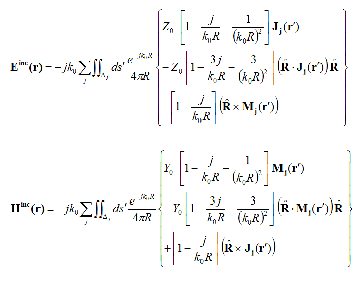
In the physical optics domain, the known equivalent electric and magnetic surface currents (or indeed the known tangential E and H field components) over a given closed surface S can be used to find reradiated electric and magnetic fields everywhere in the space as follows:
where the summation over index j is carried out for all the elementary cells Δj that make up the Huygens box. In EM.Cube Huygens surfaces are cubic and are discretized using a rectangular mesh. Therefore, Δj represents any rectangular cell located on one of the six faces of Huygens box. Note that the calculated near-zone electric and magnetic fields act as incident fields for the scatterers in your PO Module project. The Huygens source data are normally generated in one of EM.Cube's full-wave computational modules like FDTD, Planar or MoM3D. Keep in mind that the fields scattered (or reradiated) by your physical structure do not affect the fields inside the Huygens source.
The far fields of the Huygens surface currents are calculated from the following relations:
Physical Structure & Its Discretization
Grouping Objects By Surface Type
EM.Cube's Physical Optics (PO) Module organizes physical objects by their surface type. A regular object is assumed to be made of one of the three surface types:
- Perfect Electric Conductor (PEC)
- Perfect Magnetic Conductor (PMC)
- Generalized Impedance Surface
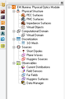
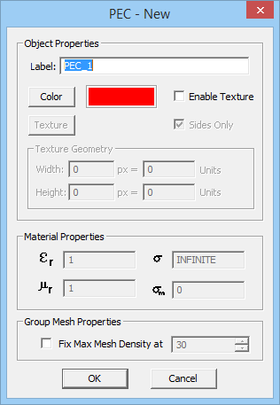
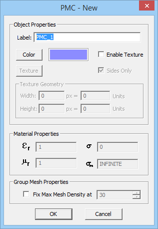
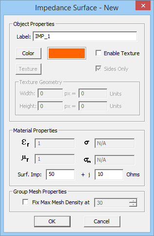
PO Module can only handle surface and solid objects. No curve objects are allowed in the project workspace; or else, they will be ignored during the PO simulation. You can define several PEC, PMC or impedance surface groups with different colors and impedance values (for the last type). All the objects created and drawn under a group share the same color and other properties. A new surface group can be defined by simply right clicking on one of the three PEC, PMC or Impedance Surface items in the Physical Structure section of the Navigation Tree and selecting Insert New PEC..., Insert New PMC..., or Insert New Impedance Surface... from the contextual menu. A dialog for setting up the group properties opens up. In this dialog you can change the name of the group or its color. In the case of a surface impedance group, you can set the values for the real and imaginary parts of the Surface Impedance in Ohms.
Figure 1: PO Module's Navigation Tree and its PEC, PMC and Impedance Surface dialogs.
Creating New Objects & Moving Them Around
The objects that you draw in EM.Cube's project workspace always belong to the "Active" surface group. By default, the last object group that you created remains active until you change it. The current active group is always listed in bold letters in the Navigation Tree. Any surface group can be made active by right clicking on its name in the Navigation Tree and selecting the Activate item of the contextual menu. If you start a new PO Module project and draw any object without having previously defined a surface group, a default PEC group is automatically created and added to the Navigation Tree to hold your new object.
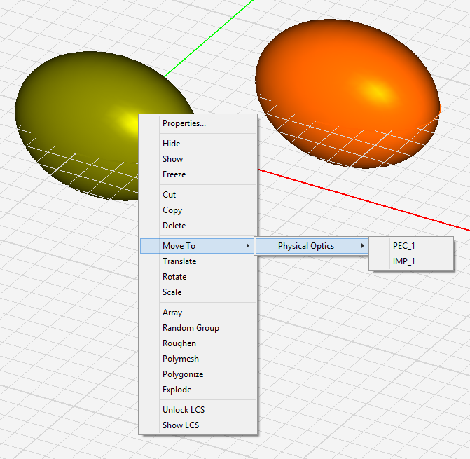
You can move one or more selected objects to any material group. Right click on the highlighted selection and select Move To > Physical Optics > from the contextual menu. This opens another sub-menu with a list of all the available surface groups already defined in PO Module. Select the desired surface group, and all the selected objects will move to that group. The objects can be selected either in the project workspace, or their names can be selected from the Navigation Tree. In the latter case, make sure that you hold the keyboard's Shift Key or Ctrl Key down while selecting a material group's name from the contextual menu. You can also move one or more objects from a PO surface group to EM.Cube's other modules, or vice versa. In that case, the sub-menus of the Move To > item of the contextual menu will indicate all the EM.Cube modules that have valid groups for transfer of the selected objects.
| |
In EM.Cube, you can import external CAD models (such as STEP, IGES, STL models, etc.) only to CubeCAD. From CubeCAD, you can then move the imported objects to any other computational module including PO Module. |
Figure 1: Moving objects between different surface groups in PO Module.
Generating & Customizing PO Mesh
The mesh generation process in PO Module involves three steps:
- Setting the mesh properties.
- Generating the mesh.
- Verifying the mesh.
The objects of your physical structure are meshed based on a specified mesh density expressed in cells/λ0. The default mesh density is 20 cells/λ0. To view the PO mesh, click on the ![]() button of the Simulate Toolbar or select Menu > Simulate > Discretization > Show Mesh or use the keyboard shortcut Ctrl+M. When the PO mesh is displayed in the project workspace, EM.Cube's mesh view mode is enabled. In this mode, you can perform view operations like rotate view, pan, zoom, etc. However, you cannot select or move or edit objects. While the mesh view is enabled, the Show Mesh
button of the Simulate Toolbar or select Menu > Simulate > Discretization > Show Mesh or use the keyboard shortcut Ctrl+M. When the PO mesh is displayed in the project workspace, EM.Cube's mesh view mode is enabled. In this mode, you can perform view operations like rotate view, pan, zoom, etc. However, you cannot select or move or edit objects. While the mesh view is enabled, the Show Mesh ![]() button remains depressed. To get back to the normal view or select mode, click this button one more time, or deselect Menu > Simulate > Discretization > Show Mesh to remove its check mark or simply click the Esc Key of the keyboard.
button remains depressed. To get back to the normal view or select mode, click this button one more time, or deselect Menu > Simulate > Discretization > Show Mesh to remove its check mark or simply click the Esc Key of the keyboard.
"Show Mesh" generates a new mesh and displays it if there is none in the memory, or it simply displays an existing mesh in the memory. This is a useful feature because generating a PO mesh may take a long time depending on the complexity and size of objects. If you change the structure or alter the mesh settings, a new mesh is always generated. You can ignore the mesh in the memory and force EM.Cube to generate a mesh from the ground up by selecting Menu > Simulate > Discretization > Regenerate Mesh or by right clicking on the 3-D Mesh item of the Navigation Tree and selecting Regenerate from the contextual menu.
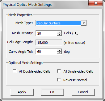
To set the PO mesh properties, click on the ![]() button of the Simulate Toolbar or select Menu > Simulate > Discretization > Mesh Settings... or right click on the 3-D Mesh item in the Discretization section of the Navigation Tree and select Mesh Settings... from the contextual menu, or use the keyboard shortcut Ctrl+G. You can change the value of Mesh Density to generate a triangular mesh with a higher or lower resolutions. PO Module offers two algorithms for triangular mesh generation. The default algorithm is Regular Surface Mesh, which creates triangular elements that have almost equal edge lengths. The other algorithm is Structured Surface Mesh, which usually creates a very structured mesh with a large number of aligned triangular elements. You can change the mesh generation algorithm from the dropdown list labeled Mesh Type. Another parameter that can affect the shape of the mesh especially in the case of solid objects is the Curvature Angle Tolerance expressed in degrees. This parameter determines the apex angle of the triangular cells of the structured mesh. Lower values of the angle tolerance will results in more pointed triangular cells.
button of the Simulate Toolbar or select Menu > Simulate > Discretization > Mesh Settings... or right click on the 3-D Mesh item in the Discretization section of the Navigation Tree and select Mesh Settings... from the contextual menu, or use the keyboard shortcut Ctrl+G. You can change the value of Mesh Density to generate a triangular mesh with a higher or lower resolutions. PO Module offers two algorithms for triangular mesh generation. The default algorithm is Regular Surface Mesh, which creates triangular elements that have almost equal edge lengths. The other algorithm is Structured Surface Mesh, which usually creates a very structured mesh with a large number of aligned triangular elements. You can change the mesh generation algorithm from the dropdown list labeled Mesh Type. Another parameter that can affect the shape of the mesh especially in the case of solid objects is the Curvature Angle Tolerance expressed in degrees. This parameter determines the apex angle of the triangular cells of the structured mesh. Lower values of the angle tolerance will results in more pointed triangular cells.
Figure 1: PO Module's Mesh Settings dialog.
More On Triangular Surface Mesh
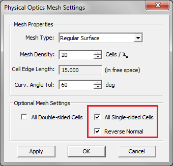
The physical optics method assumes an unbounded, open-boundary computational domain, wherein the physical structure is placed against a free space background medium. As such, only finite-extent surfaces are discretized. EM.Cube's PO Module uses a triangular surface mesh to discretize all the surface and solid objects in the project workspace. As mentioned earlier, curve objects (or wires) are not allowed in PO Module. In the case of solids, only the surface of the object or its faces are discretized, as the interior volume is not taken into account in a PO analysis. In general, triangular cells are placed on the exterior surface of solid objects. In contrast, surface objects are assumed to be double-sided by default. The means that the PO mesh of a surface object indeed consists of coinciding double cells, one representing the upper or positive side and the other representing the lower or negative side. This may lead to a very large number of cells. EM.Cube's PO mesh has some more settings that allow you to treat all mesh cells as double-sided or all single-sided. This can be done in the Mesh Settings dialog by checking the boxes labeled All Double-Sided Cells and All Single-Sided Cells. This is useful when your project workspace contains well-organized and well-oriented surface objects only. In the single-sided case, it is very important that all the normals to the cells point towards the source. Otherwise, the surface objects will be assumed to lie in the shadow region and no currents will be computed on them. By checking the box labeled Reverse Normal, you instruct EM.Cube to reverse the direction of the normal vectors at the surface of all the cells.
Figure: Forcing mesh cells to be single-sided in a PO simulation.
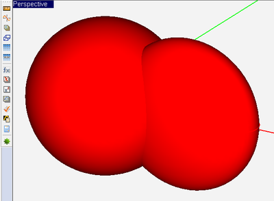
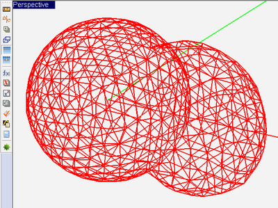
As a general rule, EM.Cube's PO mesh generator merges all the objects that belong to the same surface group using the Boolean Union operation. As a result, overlapping objects are transformed into a single consolidated object. This is particularly important for generating a contiguous and consistent mesh in the transition and junction areas between connected objects. In general, objects of the same CAD category can be "unioned". For example, surface objects can be merged together, and so can solid objects. However, a surface object and a solid in general do not merge. Objects that belong to different groups on the Navigation Tree are not merged during mesh generation even if they are all of PEC type and physically overlap.
Figure: Geometry and PO mesh of an overlapping sphere and ellipsoid.
Mesh Density & Local Mesh Control
EM.Cube's PO Module applies the mesh density specified in the Mesh Settings dialog on a global scale to discretize all the objects in the project workspace. Although the mesh density is expressed in cells per free space wavelength similar to full-wave method of moments (MoM) solvers, you have to keep in mind that the triangular surface mesh cells in PO Modules act slightly differently. The complex-valued, vectorial, electric and magnetic surface currents, J and M are assumed to be constant on the surface of each triangular cell. On plates and flat faces or surfaces, the normal vectors to all the cells are identical. Incident plane waves or other types of relatively uniform source fields induce uniform PO currents on all these cells. Therefore, a high resolution mesh may not be necessary on flat surface or faces. However, a high mesh density is very important for accurate discretization of curved objects like spheres or ellipsoids.
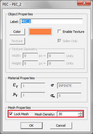
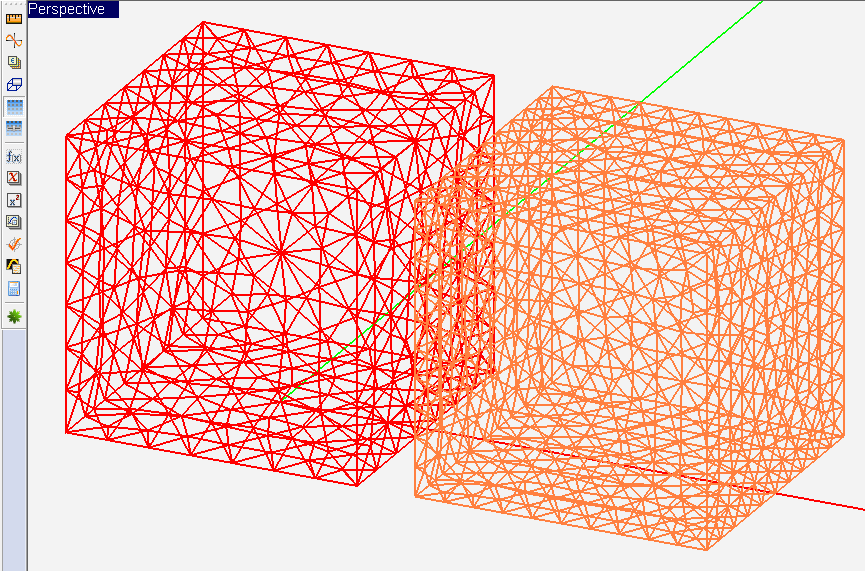
You can lock the mesh density of any surface group to any desired value different than the global mesh density. To do so, open the property dialog of a surface group by right clicking on its name in the Navigation Tree and select Properties... from the contextual menu. At the bottom of the dialog, check the box labeled Lock Mesh. This will enable the Density box, where you can set a desired value. The default value is equal to the global mesh density.
Figure 1: Locking the mesh density of a PEC group.
Figure 2: Triangular surface mesh of two PEC box objects with the orange PEC group having a locked mesh of higher density.
Excitation Sources
Hertzian Dipole Sources
A short dipole is the simplest way of exciting a structure in EM.Cube's PO Module. A short dipole source acts like an infinitesimally small ideal current source. To define a short dipole source, follow these steps:
- Right click on the Short Dipoles item in the Sources section of the Navigation Tree and select Insert New Source... from the contextual menu. The Short Dipole dialog opens up.
- In the Source Location section of the dialog, you can set the coordinate of the center of the short dipole. By default, the source is placed at the origin of the world coordinate system at (0,0,0). You can type in new coordinates or use the spin buttons to move the dipole around.
- In the Source Properties section, you can specify the Amplitude in Volts, the Phase in degrees as well as the Length of the dipole in project units.
- In the Direction Unit Vector section, you can specify the orientation of the short dipole by setting values for the components uX, uY, and uZ of the dipole's unit vector. The default values correspond to a vertical (Z-directed) short dipole. The dialog normalizes the vector components upon closure even if your component values do not satisfy a unit magnitude.
Importing Short Dipoles From MoM3D Module
The solution of a problem in one of EM.Cube's computational modules can serve as the excitation source for another problem in another computational module. An example of this is analyzing a wire antenna in the MoM3D Module and importing the wire current solution to PO Module to excite a large scatterer. Remember that you cannot define wires or curve objects in PO Module. However, you can have short dipole sources that act like differential wire elements carrying fixed currents. Using this concept, you can realize a complex wire antenna or radiator array as the source of your PO project.
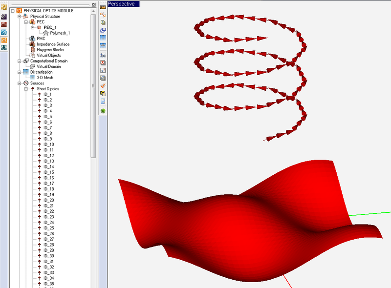
When you simulate a wire structure in the MoM3D Module, you can define a Current Distribution Observable in your project. This is used not only to visualize the current distribution in the project workspace, but also to save the current solution into an ASCII data file. This data file is called "MoM.IDI" by default and has a .IDI file extension. The current data are saved as line segments representing each of the wire cells together with the complex-valued, vectorial current at the center of each cell. You can import the current data from an existing .IDI file to PO Module, To import a wire current solution, right click on Short Dipoles item in the Sources section of the Navigation Tree and select Import Dipole Source... from the contextual menu. This opens up the standard Windows Open dialog with the file type set to .IDI. Browse your folders to find the right current data file. Once you find it, select it and click the Open button of the dialog. This will create as many short dipole sources on the PO Module's Navigation Tree as the total number of mesh cells in the Wire MoM solution. From this point on, each of the imported dipoles behave like a regular short dipole source. You can open the property dialog of each individual source and modify its parameters, if necessary.
Figure: Importing a Wire MoM current solution into the PO Module. In this structure, 90 wire cell currents representing a helical antenna were imported and placed above a large sinusoidal PEC surface.
Plane Wave Sources
Your physical structure in PO Module can be excited by an incident plane wave. In particular, a plane wave source can be used to compute the radar cross section of a target. A plane wave is defined by its propagation vector indicating the direction of incidence and its polarization. EM.Cube's PO Module provides the following polarization options:
- TMz
- TEz
- Custom Linear
- LCPz
- RCPz
The direction of incidence is defined through the θ and φ angles of the unit propagation vector in the spherical coordinate system. The values of these angles are set in degrees in the boxes labeled Theta and Phi. The default values are θ = 180° and φ = 0° representing a normally incident plane wave propagating along the -Z direction with a +X-polarized E-vector. In the TMz and TEz polarization cases, the magnetic and electric fields are parallel to the XY plane, respectively. The components of the unit propagation vector and normalized E- and H-field vectors are displayed in the dialog. In the more general case of custom linear polarization, besides the incidence angles, you have to enter the components of the unit electric Field Vector. However, two requirements must be satisfied: ê . ê = 1 and ê × k = 0 . This can be enforced using the Validate button at the bottom of the dialog. If these conditions are not met, an error message is generated. The left-hand (LCP) and right-hand (RCP) circular polarization cases are restricted to normal incidences only (θ = 180°).
To define a plane wave source follow these steps:
- Right click on the Plane Waves item in the Sources section of the Navigation Tree and select Insert New Source... The Plane wave Dialog opens up.
- In the Field Definition section of the dialog, you can enter the Amplitude of the incident electric field in V/m and its Phase in degrees. The default field Amplitude is 1 V/m with a zero Phase.
- The direction of the Plane Wave is determined by the incident Theta and Phi angles in degrees. You can also set the Polarization of the plane wave and choose from the five options described earlier. When the Custom Linear option is selected, you also need to enter the X, Y, Z components of the E-Field Vector.
Huygens Sources
At the end of a full-wave simulation in the EM.Cube's FDTD, MoM3D, Planar or Physical Optics Modules, you can generate Huygens surface data. According to Huygens' principle, if one knows the tangential electric and magnetic field components on a closed surface, one can determine the total electric and magnetic fields everywhere inside and outside that closed surface. Huygens surfaces are defined around a structure for recording the tangential components of electric and magnetic fields at the end of full-wave simulation of the structure. The tangential electric and magnetic fields are saved into ASCII data files as magnetic and electric currents, respectively. These current can be used as excitation for other structures. In other words, the electric and magnetic currents associated with a Huygens source radiate energy and provide the excitation for the PO Module's physical structure.
In order to define a Huygens source, you need to have a Huygens data file of .HUY type. This file is generated as an output data file at the end of an FDTD, MoM3D, Planar or PO simulation, if you have defined a Huygens Surface observable in one of those projects. When you define a Huygens source, you indeed import an existing Huygens surface into the project and set it as an excitation source.
To create a new Huygens source, follow these steps:
- Right click on the Huygens Sources item in the Sources section of the Navigation Tree and select Import Huygens Source... from the contextual menu.
- The standard Windows Open Dialog opens up. The file type is set to .HUY by default. Browse your folders to find a Huygens surface data file with a .HUY file extension. Select the file and click the Open button of the dialog to import the data.
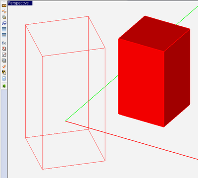
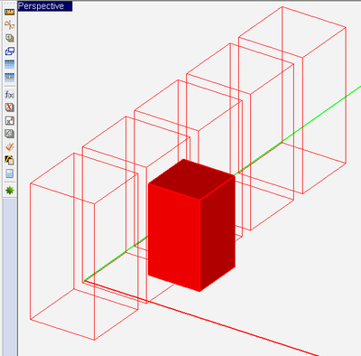
- Once imported, the Huygens source appears in the Project Workspace as a wire-frame box.
- You can open the property dialog of a Huygens source by right clicking on its name in the Navigation Tree and selecting Properties... From this dialog you can change the color of the Huygens source box as well as its location and orientation. You can enter new values for the X, Y, Z Center Coordinates and Rotation Angles of the Huygens box. You can also view the dimensions of the box.
- By default, the Huygens data are imported as a single Huygens source. You can create an arbitrary array of Huygens sources for your PO project. To do so, in the "Create Array" section of the Huygens source dialog, enter desired values for the Number of Elements and Element Spacing along the X, Y and Z directions. You will see an array of wire-frame box appear in the project workspace.
Figure: (Left) A rotated imported Huygens source, and (Right) An array of imported Huygens sources defined to excite a PEC box.
Running PO Simulations
Running A Basic PO Analysis
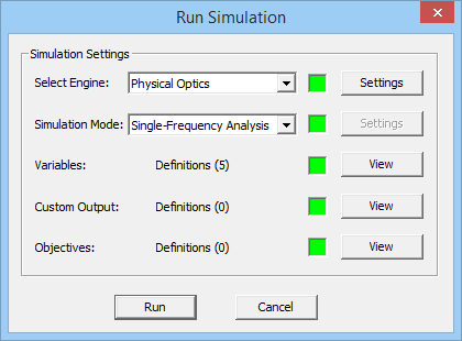
To open PO Module's Simulation Run dialog, click the Run ![]() button of the Simulate Toolbar or select Menu > Simulate > Run...or use the keyboard shortcut Ctrl+R. To start the simulation click the Run button of this dialog. Once the PO simulation starts, a new dialog called Output Window opens up that reports the various stages of PO simulation, displays the running time and shows the percentage of completion for certain tasks during the PO simulation process. A prompt announces the completion of the PO simulation. At this time, EM.Cube generates a number of output data files that contain all the computed simulation data. These include current distributions, near field data, far field radiation pattern data as well bi-static or mono-static radar cross sections (RCS) if the structure is excited by a plane wave source.
button of the Simulate Toolbar or select Menu > Simulate > Run...or use the keyboard shortcut Ctrl+R. To start the simulation click the Run button of this dialog. Once the PO simulation starts, a new dialog called Output Window opens up that reports the various stages of PO simulation, displays the running time and shows the percentage of completion for certain tasks during the PO simulation process. A prompt announces the completion of the PO simulation. At this time, EM.Cube generates a number of output data files that contain all the computed simulation data. These include current distributions, near field data, far field radiation pattern data as well bi-static or mono-static radar cross sections (RCS) if the structure is excited by a plane wave source.
Figure 1: PO Module's Simulation Run dialog.
Setting The Numerical Parameters
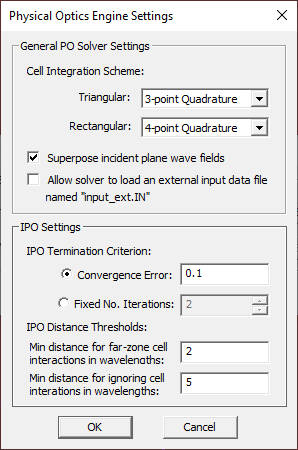
Before you run a PO simulation, you can change some of the PO simulation engine settings. While in the PO Module's Simulation Run Dialog, click the Settings button next to the Select Engine dropdown list. In the Physical Optics Engine Settings Dialog, there are two options for Solver Type: Iterative and GOPO. The default option is Iterative. The GOPO solver is a zero-order PO simulator that uses Geometrical Optics (GO) to determine the lit and shadow cells in the structure's mesh. For the termination of the IPO solver, there are two options: Convergence Error and Maximum Number of Iterations. The default Termination Criterion is based on convergence error, which has a default value of 0.1 and can be changed to any desired accuracy. The convergence error is defined as the L2 norm of the normalized residual error in the combined J/M current solution of the entire discretized structure from one iteration to the next. Note that for this purpose, the magnetic currents are scaled by η0 in the residual error vector.
You can also use higher- or lower-order integration schemes for the calculation of field integrals. EM.Cube's PO simulation engine uses triangular cells for the mesh of the physical surface structures and rectangular cells for discretization of Huygens sources and surfaces. For integration of triangular cells, you have three options: 7-Point Quadrature, 3-Point Quadrature and Constant. For integration of rectangular cells, too, you have three options: 9-Point Quadrature, 4-Point Quadrature and Constant.
Figure 1: PO Module's Simulation Engine Settings dialog.
Visualizing Current Distributions
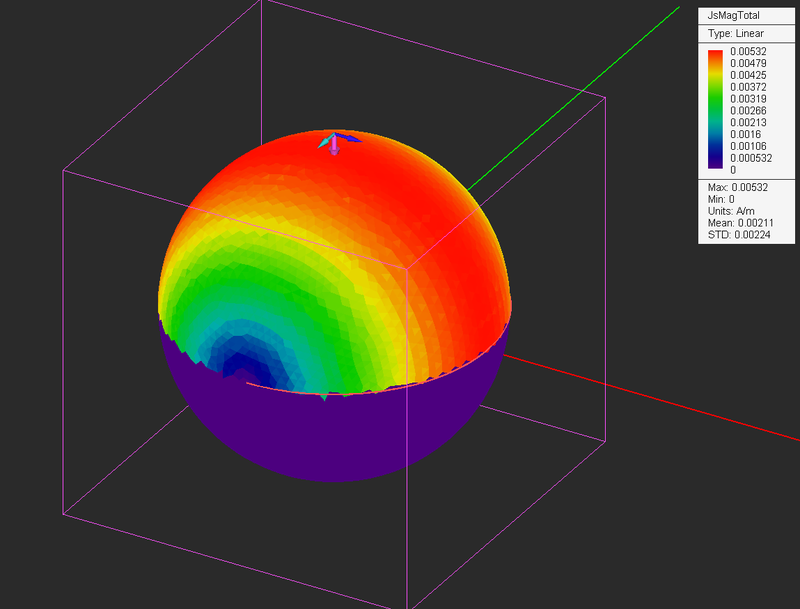
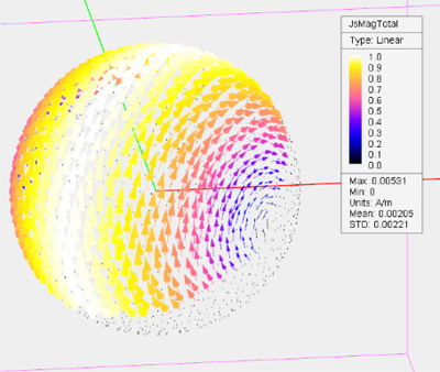
At the end of a PO simulation, EM.Cube's PO engine generates a number of output data files that contain all the computed simulation data. The main output data are the electric and magnetic current distributions. You can easily examine the 3D color-coded intensity plots of current distributions in the project workspace. Current distributions are visualized on the surface of the PO mesh cells, and the magnitude and phase of the electric and magnetic surface currents are plotted for all the objects. In order to view these currents, you must first define a current distribution observable before running the PO simulation. To do this, right click on the Current Distributions item in the Observables section of the Navigation Tree and select Insert New Observable.... The Current Distribution Dialog opens up. Accept the default settings and close the dialog. A new current distribution node is added to the Navigation Tree. Unlike the Planar Module, in the PO Module you can define only one current distribution node in the Navigation Tree, which covers all the objects in the project workspace. After a PO simulation is completed, new plots are added under the current distribution node of the Navigation Tree. Separate plots are produced for the magnitude and phase of each of the electric and magnetic surface current components (X, Y and Z) as well as the total current magnitude. The magnitude maps are plotted on a normalized scale with the minimum and maximum values displayed in the legend box. The phase maps are plotted in radians between -p and p. Note that sometimes the current distribution plots may hide inside smooth and curved objects, and you cannot see them. You may have to freeze such objects or switch to the mesh view mode.
Figure: The current distribution plot of a PEC sphere illuminated by an obliquely incident plane wave.
Near Field Visualization
EM.Cube allows you to visualize the near fields at a specific field sensor plane. Calculation of near fields is a post-processing process and may take a considerable amount of time depending on the resolution that you specify. To define a new Field Sensor, follow these steps:
- Right click on the Field Sensors item in the Observables section of the Navigation Tree and select Insert New Observable...
- The Label box allows you to change the sensor’s name. you can also change the color of the field sensor plane using the Color button.
- Set the Direction of the field sensor. This is specified by the normal vector of the sensor plane. The available options are X, Y and Z, with the last being the default option.
- By default EM.Cube creates a field sensor plane passing through the origin of coordinates (0,0,0) on the XY plane. You can change the location of the sensor plane to any point by typing in new values for the X, Y and Z Center Coordinates. You can also change these coordinates using the spin buttons.
- The initial size of the sensor plane is 100 × 100 project units. You can change the dimensions of the sensor plane to any desired size. You can also set the Number of Samples along the different directions. These numbers determine the resolution of near field maps. Keep in mind that large numbers of samples may result in long computation times.
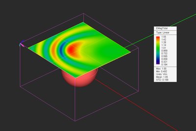
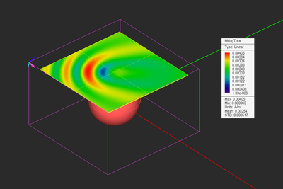
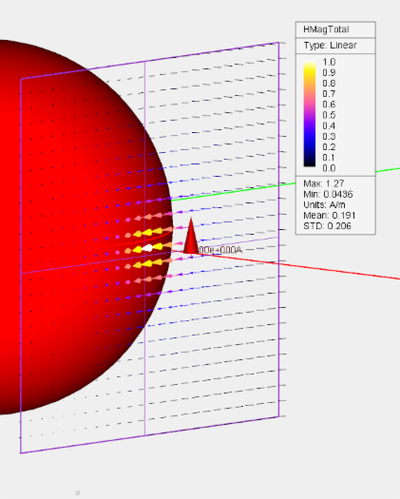
After closing the Field Sensor Dialog, a new field sensor item immediately appears under the Observables section in the Navigation Tree. Once a PO simulation is finished, a total of 14 plots are added to every field sensor node in the Navigation Tree. These include the magnitude and phase of all three components of E and H fields and the total electric and magnetic field values. Click on any of these items and a color-coded intensity plot of it will be visualized on the project workspace. A legend box appears in the upper right corner of the field plot, which can be dragged around using the left mouse button. The values of the magnitude plots are normalized between 0 and 1. The legend box contains the minimum field value corresponding to 0 of the color map, maximum field value corresponding to 1 of the color map, and the unit of the field quantity, which is V/m for E-field and A/m for H-field. The values of phase plots are always shown in Radians between -p and p.To display the fields properly, the structure is cut through the field sensor plane, and only part of it is shown. If the structure still blocks your view, you can simply hide or freeze it. You can change the view of the field plot with the available view operations such as rotate view, pan, zoom, etc.
Figure 2: Near field plots of electric and magnetic fields on a sensor plane.
Visualizing 3D Radiation Patterns
Unlike the FDTD method, Physical Optics is an open-boundary technique. You do not need a far field box to perform near-to-far-field transformations. Nonetheless, you still need to define a far field observable if you want to plot radiation patterns. A far field can be defined by right clicking on the Far Fields item in the Observables section of the Navigation Tree and selecting Insert New Radiation Pattern... from the contextual menu. The Radiation Pattern dialog opens up. You can accept most of the default settings in this dialog. The Output Settings section allows you to change the Angle Increment in the degrees, which sets the resolution of far field calculations. The default value is 5 degrees. After closing the radiation pattern dialog, a far field entry immediately appears with its given name under the Far Fields item of the Navigation Tree.
After a PO simulation is finished, three radiation patterns plots are added to the far field node in the Navigation Tree. These are the far field component in θ direction, the far field component in φ direction and the total far field defines as:
- [math]|\mathbf{E_{ff,tot}}| = \sqrt{ |E_{\theta}|^2 + |E_{\phi}|^2 }[/math]
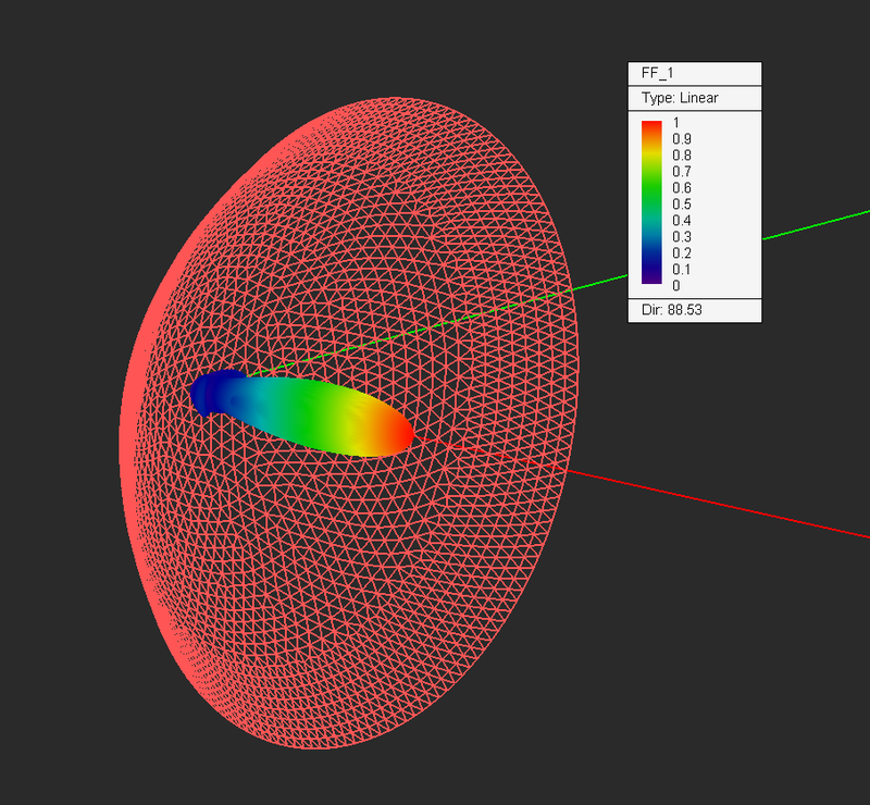
The 3D plots can be viewed by clicking on their name in the navigation tree. They are displayed in EM.Cube's project workspace and are overlaid on the project's structure. The view of a 3D radiation pattern plots can be changed with the available view operations such as rotate view, pan, zoom, etc. If the structure blocks the view of the pattern, you can simply hide the whole structure or parts of it. The fields are always normalized to the maximum of the total far field. A legend box appears in the upper right corner of the 3D radiation plot, which can be moved around by clicking and dragging with the left mouse button. The calculated Directivity of the radiating structure is displayed at the bottom of the legend box. It is important to note that if the PO structure is excited by an incident plane wave, the radiation patterns indeed represent the far-zone scattered field data.
Figure: 3D radiation pattern of a parabolic dish reflector excited by a short dipole at its focal point.
Radar Cross Section
When the physical structure is excited by a plane wave source, the calculated far field data indeed represent the scattered fields. EM.Cube calculates the radar cross section (RCS) of a target, which is defined in the following manner:
- [math] \sigma_{\theta} = 4\pi r^2 \dfrac{ \big| \mathbf{E}_{\theta}^{scat} \big| ^2} {\big| \mathbf{E}^{inc} \big|^2}, \quad \sigma_{\phi} = 4\pi r^2 \dfrac{ \big| \mathbf{E}_{\phi}^{scat} \big| ^2} {\big| \mathbf{E}^{inc} \big|^2}, \quad \sigma = \sigma_{\theta} + \sigma_{\phi} = 4\pi r^2 \dfrac{ \big| \mathbf{E}_{tot}^{scat} \big| ^2} {\big| \mathbf{E}^{inc} \big|^2} [/math]
Three RCS quantities are computed: the θ and φ components of the radar cross section as well as the total radar cross section, which are dented by σθ, σφ, and σtot. In addition, EM.Cube's PO Module calculates two types of RCS for each structure: Bi-Static RCS and Mono-Static RCS. In bi-static RCS, the structure is illuminated by a plane wave at incidence angles θ0 and φ0, and the RCS is measured and plotted at all θ and φ angles. In mono-static RCS, the structure is illuminated by a plane wave at incidence angles θ0 and φ0, and the RCS is measured and plotted at the echo angles 180°-θ0; and φ0. It is clear that in the case of mono-static RCS, the PO simulation engine runs an internal angular sweep, whereby the values of the plane wave incidence angles θ and φ are varied over the entire intervals [0°, 180°] and [0°, 360°], respectively, and the backscatter RCS is recorded.
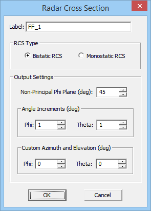
To calculate RCS, first you have to define an RCS observable instead of a radiation pattern. Right click on the Far Fields item in the Observables section of the Navigation Tree and select Insert New RCS... to open the Radar Cross Section Dialog. Use the Label box to change the name of the far field or change the color of the far field box using the Color button. Select the type of RCS from the two radio buttons labeled Bi-Static RCS and Mono-Static RCS. The former is the default choice. The resolution of RCS calculation is specified by Angle Increment expressed in degrees. By default, the θ and φ angles are incremented by 5 degrees. At the end of a PO simulation, besides calculating the RCS data over the entire (spherical) 3D space, a number of 2D RCS graphs are also generated. These are RCS cuts at certain planes, which include the three principal XY, YZ and ZX planes plus one additional constant f-cut. This latter cut is at f = 45° by default. You can assign another azimuth angle in degrees in the box labeled Non-Principal Phi Plane.
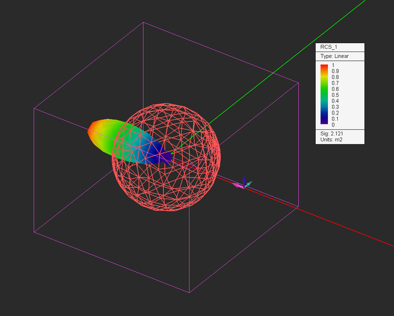
At the end of a PO simulation, the thee RCS plots σθ, σφ, and σtot are added under the far field section of the Navigation Tree. These plots are very similar to the three 3D radiation pattern plots. You can view them by clicking on their names in the navigation tree. The RCS values are expressed in m2. For visualization purposes, the 3D plots are normalized to the maximum RCS value, which is also displayed in the legend box. Keep in mind that computing the 3D mono-static RCS may take an enormous amount of computation time.
Figure: RCS of a PEC sphere illuminated by an laterally incident plane wave.
Customizing 3D Plots
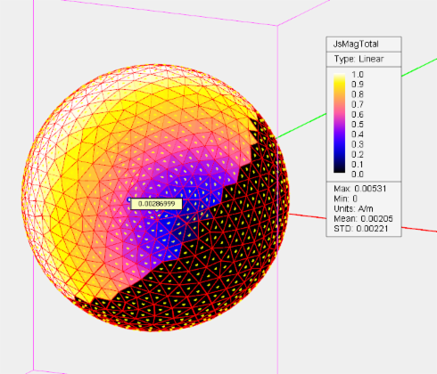
EM.CUBE's current distribution plots are interactive. When you move the mouse over a current plot, tiny dots appear on its surface. These dots correspond to the points on the sensor plane where the current data have been calculated. Upon mouse-over, you can highlight one of these points. A small tooltip appears on the plot that shows the current value at that point. In other words, you can read the plot values using mouse-over. The legend of a current plot also shows the minimum and maximum current values, the current unit (A/m on metallic traces, V/m on slot traces and A/m2 on embedded objects) as well as the mean current and the standard deviation.
Figure: Reading current values from a current distribution map by mouse-over.
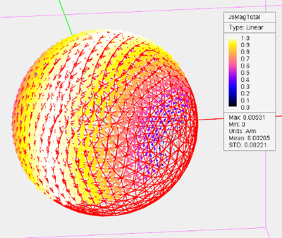
EM.CUBE offers two different ways of visualizing electric and magnetic current distributions: as a confetti plot or a cone plot. The first type is a scalar intensity plot and shows the current amplitude and phase using colored triangular mesh cells. The second type is a vectorial plot showing cones (or arrows) directed along the visualized current component. In the case of the total electric current distribution, the cone plot shows the overall direction of the currents at any point on the surface of objects. To set the type of a current plot, open the current distribution plot's property dialog by right clicking its name in the Navigation Tree and selecting Properties... from the contextual menu. In the Plot Type section, choose one of the two radio buttons labeled Confetti or Cone. In the latter case, you can set the size of the vector cones using the box labeled Max Size. You can set the plot type at the time of defining the current distribution before running the PO simulation. You can also change the plot type afterwards and switch between the confetti and cone types back and forth.
Figure: A vectorial (cone-type) current distribution plot of the PEC sphere: (Left) overlaid on mesh and (Right) with the sphere object frozen.
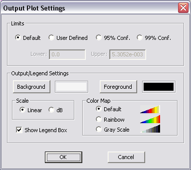
Current distribution maps are displayed with some default settings and options. You can customize the individual maps (total, magnitude, phase, etc.). To do so, open the Output Plot Settings Dialog by right clicking on the specific plot entry in the Navigation Tree and selecting Properties... or by double clicking on the surface of the plot's legend box. Two scale options are available: Linear and dB. With the Linear (default) option selected, the current value is always normalized to the maximum total current in that plane, and the normalized scale is mapped between the minimum and maximum values. If the dB option is selected, the normalized current is converted to dB scale. The plot limits (bounds) can be set individually for every current distribution plot. In the Limits section of the plot's property dialog, you see four options: Default, User Defined, 95% Conf. and 95% Conf.. Select the user defined option and enter new values for the Lower and Upper limits. The last two options are used to remove the outlier data within the 95% and 99% confidence intervals, respectively. In other words, the lower and upper limits are set to ? ± 1.96? and ? ± 2.79? , respectively, assuming a normal distribution of the data. Three color maps are offered: Default, Rainbow and Grayscale. You can hide the legend box by deselecting the box labeled Show Legend Box. You can also change the foreground and background colors of the legend box.
Figure: The output plot settings dialog.
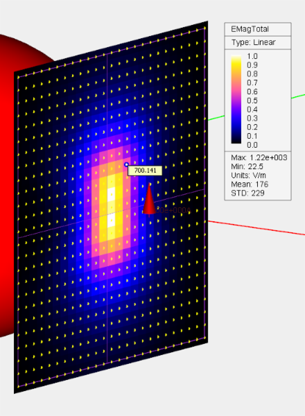
EM.CUBE's field plots are interactive. When you move the mouse over a field plot, tiny dots appear on its surface. These dots correspond to the points on the sensor plane where the field data have been calculated. Upon mouse-over, you can highlight one of these points. A small tooltip appears on the plot that shows the field value at that point. In other words, you can read the plot values using mouse-over. The legend of a field plot also shows the minimum and maximum field values, the field unit (V/m for electric and A/m for magnetic) as well as the mean field and the standard deviation.
Figure: Reading field values form a 3-D sensor plot using mouse-over.
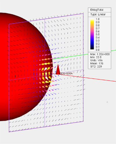
EM.CUBE offers two different ways of visualizing electric and magnetic fields: as a confetti plot or a cone plot. The first type is a scalar intensity plot and shows the field amplitude and phase using small colored pixels whose size is depends on the total size of the sensor plane and its number of samples. The second type is a vectorial plot showing cones (or arrows) directed along the visualized field component. In the case of the total electric and magnetic fields, the cone plots show the overall direction of the fields at any point on the sensor plane. To set the type of a field plot, open the field sensor's property dialog by right clicking its name in the Navigation Tree and selecting Properties... from the contextual menu. In the Plot Type section, choose one of the two radio buttons labeled Confetti or Cone. In the latter case, you can set the size of the vector cones using the box labeled Max Size. You can set the plot type at the time of defining the field sensor before running the PO simulation. You can also change the plot type afterwards and switch between the confetti and cone types back and forth.
Figure: Vectorial visualization of the electric and magnetic fields: (Left) E-field, (Right) H-field.
Similar to current distribution plots, field plots (total, magnitude, phase, etc.) are displayed with some default settings and options, which can be further customized individually. To do so, open the Output Plot Settings dialog by right clicking on a specific plot entry in the Navigation Tree and selecting Properties... or by double clicking on the surface of the plot's legend box. The settings are identical to those of current distribution plots. Two scale options, linear and dB, are available. You can also change the lower and upper limits of the individual field plots as well as their color map.
2D Radiation Pattern & RCS Graphs
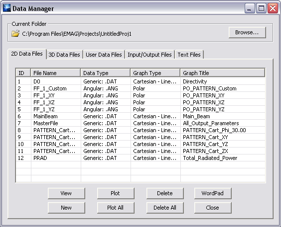
At the end of a PO simulation, the radiation pattern data Eθ, Eφ, and Etot in the three principal XY, YZ and ZX planes as well as an additional user defined phi plane cut are available for plotting on 2-D graphs. There are a total of eight 2-D pattern graphs in the data manager: 4 polar graphs and 4 Cartesian graphs of the same pattern data. To open data manager, click the Data Manager ![]() button of the Compute Toolbar or select Compute
button of the Compute Toolbar or select Compute ![]() Data Manager from the menu bar or right click on the Data Manager item of the Navigation Tree and select Open Data Manager... from the contextual menu or use the keyboard shortcut Ctrl+D. In the Data manager Dialog, you will see a list of all the data files available for plotting. These include the four polar pattern data files with a .ANG file extension and the four Cartesian pattern data file with a .DAT file extension. Select any data file by clicking and highlighting its ID in the table and then click the Plot button to plot the graph.
Data Manager from the menu bar or right click on the Data Manager item of the Navigation Tree and select Open Data Manager... from the contextual menu or use the keyboard shortcut Ctrl+D. In the Data manager Dialog, you will see a list of all the data files available for plotting. These include the four polar pattern data files with a .ANG file extension and the four Cartesian pattern data file with a .DAT file extension. Select any data file by clicking and highlighting its ID in the table and then click the Plot button to plot the graph.
At the end of a PO sweep simulation, other radiation characteristics are also computed as a function of the sweep variable (frequency, angle, or any other user defined variable). These include the Directivity (D0), Total Radiated Power (PRAD) and Directive Gain (DG) as a function of the theta and phi angles. Another radiation characteristic of interest especially in circularly polarized scenarios is the Axial Ratio. In EM.CUBE, the axial ratio is always defined in the LCPz or RCPz sense based on the X- and Y-components of the electric field. In order to calculate the directive gain or axial ratio, you have to check the boxes labeled Axial Ratio (AR) or Directive Gain (DG) in the "Additional Radiation Characteristics" section of the Radiation Pattern Dialog. Four 2-D Cartesian graphs of the axial ratio as functions of the theta angle a generated in the three principal XY, YZ and ZX planes as well as the additional user defined phi plane cut. At the end of a PO sweep simulation, the directive gain and axial ratio can also be plotted as functions of the sweep variable. In this case, either quantity needs to be computed at a fixed pair of phi and theta angles. These angles are specified in degrees as User Defined Azimuth & Elevation in the "Output Settings" section of the Radiation Pattern Dialog. The default values of the user defined azimuth and elevation are both zero corresponding to the zenith.
The 2D RCS graphs can be plotted from EM.CUBE's data manager exactly in the same way that you plot 2D radiation pattern graphs. A total of eight 2D RCS graphs are available: 4 polar and 4 Cartesian graphs for the XY, YZ, ZX and user defined plane cuts. At the end of a sweep simulation, EM.CUBE calculates some other quantities including the backscatter RCS (BRCS), forward-scatter RCS (FRCS) and the maximum RCS (MRCS) as functions of the sweep variable (frequency, angle, or any user defined variable). In this case, the RCS needs to be computed at a fixed pair of phi and theta angles. These angles are specified in degrees as User Defined Azimuth & Elevation in the "Output Settings" section of the Radar Cross Section Dialog. The default values of the user defined azimuth and elevation are both zero corresponding to the zenith.
The data manager dialog showing a list of 2-D polar and Cartesian radiation pattern graphs.
The 2-D radiation patterns in the XY, YZ and ZX plane cuts.
PO Sweep Simulations
You can run EM.Cube's PO simulation engine in the sweep mode, whereby a parameter like frequency, plane wave incident angles or a user defined variable is varied over a specified range at predetermined samples. The output data are saved into data files for visualization and plotting. EM.Cube's PO Module currently offers three types of sweep:
- Frequency Sweep
- Angular Sweep
- Parametric Sweep
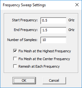
To run a PO sweep, open the Simulation 'Run Dialog' and select one of the above sweep types from the Simulation Mode dropdown list of this dialog. If you select either frequency or angular sweep, the Settings button located next to the simulation mode dropdown list becomes enabled. If you click this button, the Frequency Settings Dialog or Angle Settings Dialog opens up, respectively. In the frequency settings dialog, you can set the start and end frequencies as well as the number of frequency samples. The start and end frequency values are initially set based on the project's center frequency and bandwidth. During a frequency sweep, as the project's frequency changes, so does the wavelength. As a result, the mesh of the structure also changes at each frequency sample. The frequency settings dialog gives you three choices regarding the mesh of the project structure during a frequency sweep:
- Fix mesh at the highest frequency.
- Fix mesh at the center frequency.
- Re-mesh at each frequency.
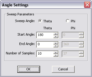
You can run an angular sweep only if your project has a plane wave excitation. In this case, you have to define a plane wave source with the default settings. During an angular sweep, either the incident theta angle or incident phi angle is varied within the specified range. The other angle remains fixed at the value that is specified in the Plane Wave Dialog. You have to select either Theta or Phi as the Sweep Angle in the Angle Settings Dialog. You also need to set the start and end angles as well as the number of angle samples.
In a parametric sweep, one or more user defined variables are varied at the same time over their specified ranges. This creates a parametric space with the total number of samples equal to the product of the number of samples for each variable. The user defined variables are defined using EM.Cube's Variables Dialog. For a description of EM.Cube variables, please refer to the "Parametric Modeling, Sweep & Optimization" section of EM.Cube Manual or see the "Parametric Sweep" sections of the FDTD or Planar Module manuals.
Figure 1: PO Module's Frequency Settings and Angle Settings dialogs.
Animation Of PO Data
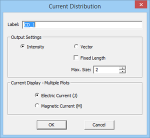
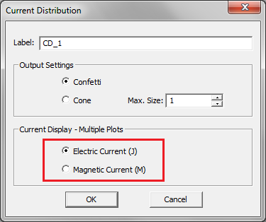
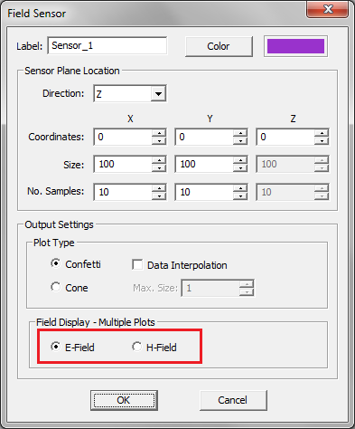
At the end of a frequency sweep, angular sweep or parametric sweep simulation in EM.Cube's PO Module, the output data are saved for visualization and plotting. In particular, if you have defined current distribution, field sensor or far field observables in your project, multiple 3D plots, as many as the total number of sweep samples, are added to the Navigation Tree. In a single simulation run, a total of 14 current distribution plots, 14 field sensor plot and 3 radiation pattern plots or 3 RCS plots are generated under every observable node defined in the Navigation Tree. However, after a sweep simulation, only one plot is saved for each sweep sample. This is done to keep the resulting plots manageable. Thus, only the total radiation pattern or total RCS are saved for each sweep sample. In the case of a current distribution observable, you have the choice to save either the magnitude of total electric current distribution |Js|or the magnitude of total magnetic current distribution |Ms|. To change this, open the Current Distribution Dialog by right clicking on the observable's name in the Navigation Tree and selecting Properties... from the contextual menu. In the Current Display - Multiple Plots section of this dialog, select one of the radio sensors labeled Electric Current (J) or Magnetic Current (M). Similarly, in the case of a field sensor observable, you have the choice to save either the total E-field magnitude plot or the total H-field magnitude plot. To change this, open the Field Sensor Dialog by right clicking on a field sensor's name in the Navigation Tree and selecting Properties... from the contextual menu. In the Field Display - Multiple Plots section of this dialog, select one of the radio sensors labeled E-Field or H-Field.
Figure 1: Selecting the current or field types for sweep data visualization in PO Module's Current Distribution and Field Sensor dialogs.
Once the sweep simulation is finished, you can click any of the field plots and visualize it in the main window. You can also animate these field plots. Animation in EM.CUBE consists of consecutive display of the plots in the main window at a preset speed. To animate the field sensor plots, right click on the field sensor's name in the Navigation Tree and select Animation from the contextual menu. The field plots start to animate beginning with the first sample, going through all the plots one by one until the last one and repeating the loop all over again. While the animation proceeds in the main window, a dialog titled Animation Controls pops up at the lower right corner of the screen. You can drag this dialog anywhere in the project workspace from its title bar. The controls dialog shows the title of each graph as it is reviewed. You can set the speed of animation by typing in a value for Rate, which is indeed the frame duration expressed in multiples of 100 milliseconds. The default frame duration is 300 msec. You can pause the animation and resume at any time. You can rewind to the first sample or skip to the last sample. You can also step through the samples one at a time using the increment (forward) or decrement (backward) buttons. To stop animation at any time, use the keyboard's Esc Key or click the Close (X) button of the animation controls dialog.
The animation controls dialog and animation of the H-field plots of a PEC sphere after an angular sweep.
