EM.Illumina
Contents
An EM.Illumina Primer
EM.Illumina in a Nutshell
EM.Illumina is a 3D electromagnetic simulator for modeling large free-space structures. It features a high frequency asymptotic solver based on Physical Optics (PO) for simulation of electromagnetic scattering from large metallic structures and impedance surfaces. You can use EM.Illumina to compute the radar cross section (RCS) of large target structures like aircraft or vehicles or simulate the radiation of antennas in the presence of large platforms.
| |
EM.Illumina is the high-frequency, asymptotic Physical Optics Module of EM.Cube, a comprehensive, integrated, modular electromagnetic modeling environment. EM.Illumina shares the visual interface, 3D parametric CAD modeler, data visualization tools, and many more utilities and features collectively known as CubeCAD with all of EM.Cube's other computational modules. |
![]() Click here to learn more about EM.Cube Modeling Environment.
Click here to learn more about EM.Cube Modeling Environment.
![]() Click here to learn more about the basic functionality of CubeCAD.
Click here to learn more about the basic functionality of CubeCAD.
Physical Optics as an Asymptotic Technique
Asymptotic methods are usually valid at high frequencies as k0 R = 2π R/λ0 >> 1, where R is the distance between the source and observation points, k0 is the free-space propagation constant and λ0 is the free-space wavelength. Under such conditions, electromagnetic fields and waves start to behave more like optical fields and waves. Asymptotic methods are typically inspired by optical analysis. Two important examples of asymptotic methods are the Shoot-and-Bounce-Rays (SBR) method and Physical Optics (PO). The SBR method is a ray tracing method based on Geometrical Optics (GO) and forms the basis of the simulation engine of EM.Terrano.
In the Physical Optics (PO) method, a scatterer surface is illuminated by an incident source, and it is modeled by equivalent electric and magnetic surface currents. This concept is based on the fundamental equivalence theorem of electromagnetics. According to the Huygens principle, the equivalent electric and magnetic surface currents are derived from the tangential components of magnetic and electric fields on a given closed surface, respectively. A simple PO analysis involves only perfect electric conductors, and only electric surface currents related to the tangential magnetic fields are considered. EM.Illumina assumes that a source like a short dipole radiator or an incident plane wave induces currents on the surface of the metallic structure. These induced currents, in turn, reradiate into the free space and produce the scattered fields. In the case of an impedance surface, both surface electric and magnetic currents are induced on the surface of the scatterer.
A challenging step in establishing the PO currents is the determination of the lit and shadow points on complex scatterer geometries. The conventional physical optics method (GO-PO) uses geometrical optics ray tracing from each source to the points on the scatterers to determine whether they fall into the lit or shadow regions. But this can become a time consuming task as the size of the computational problem grows. Besides GO-PO, EM.Illumina also offers a novel Iterative Physical Optics (IPO) solver, which dispenses with the GO part of GO-PO and automatically accounts for multiple shadowing effects using an iterative algorithm.
![]() Click here to lean more about the Theory of Physical Optics.
Click here to lean more about the Theory of Physical Optics.
Advantages & Limitations of EM.Illumina's PO Solver
EM.Illumina provides a computationally efficient alternative to full-wave solutions for extremely large structures when full-wave analysis becomes prohibitively expensive. For simple scatterer geometries, EM.Illumina's GO-PO solver is fairly adequate. But for complex geometries that involve multiple shadowing effects, the IPO solver must be utilized. The IPO technique can effectively capture dominant, near-field, multiple scattering effects from electrically large targets with concave surfaces. You have to remember that Physical Optics is a surface simulator. This is not a problem for PEC and PMC objects, which have zero internal fields, or even impedance surfaces, where you can satisfy the boundary conditions on one side of a surface only. PO analysis cannot handle the fields inside dielectric objects. Additionally, most coupling effects between adjacent scatterers are ignored.
Building the Physical Structure
Grouping Objects By Surface Type
EM.Illumina organizes physical objects by their surface type. Any object in EM.Illumina is assumed to be made of one of the three surface types:
- Perfect Electric Conductor (PEC) Surface
- Perfect Magnetic Conductor (PMC) Surface
- Generalized Impedance Surface
EM.Illumina can only handle surface and solid CAD objects. Only the outer surface of solid objects is considered in the PO simulation. No line or curve objects are allowed in the project workspace; or else, they will be ignored during the PO simulation. You can define several PEC, PMC or impedance surface groups with different colors and impedance values. All the objects created and drawn under a group share the same color and other properties.
![]() Click here to learn more about Defining a New Surface Group.
Click here to learn more about Defining a New Surface Group.
Once a new surface node has been created on the navigation tree, it becomes the "Active" surface group of the project workspace, which is always listed in bold letters. When you draw a new CAD object such as a Box or a Sphere, it is inserted under the currently active surface type. There is only one surface group that is active at any time. Any surface type can be made active by right clicking on its name in the navigation tree and selecting the Activate item of the contextual menu. It is recommended that you first create surface groups, and then draw new objects under the active surface group. However, if you start a new EM.Illumina project from scratch, and start drawing a new object without having previously defined any surface groups, a new default PEC surface group is created and added to the navigation tree to hold your new CAD object.
![]() Click here to learn more about Moving Objects among Surface Groups.
Click here to learn more about Moving Objects among Surface Groups.
| |
In EM.Cube, you can import external CAD models (such as STEP, IGES, STL models, etc.) only to CubeCAD. From CubeCAD, you can then move the imported objects to EM.Illumina. |
![]() Click here for a general discussion of Defining Materials in EM.Cube.
Click here for a general discussion of Defining Materials in EM.Cube.
Discretizing the Physical Structure
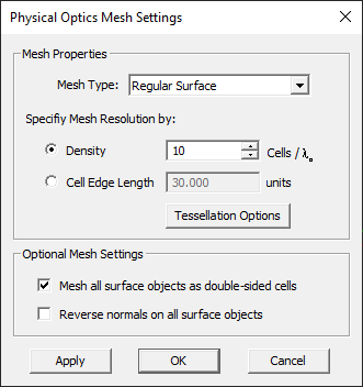
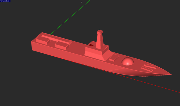
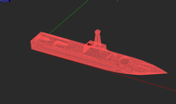
EM.Illumina uses a triangular surface mesh to discretize the structure of your project workspace. The mesh generating algorithm tries to generate regularized triangular cells with almost equal surface areas across the entire structure. You can control the cell size using the "Mesh Density" parameter. By default, the mesh density is expressed in terms of the free-space wavelength. The default mesh density is 10 cells per wavelength. In the Physical Optics method, the electric and magnetic surface currents, J and M, are assumed to be constant on the surface of each triangular cell. On flat surfaces, the unit normal vectors to all the cells are identical. Incident plane waves or other relatively uniform source fields induce uniform PO currents on all these cells. Therefore, a high resolution mesh may not be necessary on flat surface or faces. Accurate discretization of curved objects like spheres or ellipsoids, however, requires a high mesh density.
Since EM.Illumina is a surface simulator, only the exterior surface of solid CAD objects is discretized, as the interior volume is not taken into account in a PO analysis. By contrast, surface CAD objects are assumed to be double-sided. In other words, the default PO mesh of a surface object consists of coinciding double cells, one representing the upper or positive side and the other representing the lower or negative side. This may lead to a very large number of cells. EM.Illumina's mesh generator has settings that allow you to treat all mesh cells as double-sided or all single-sided. You can do that in the Mesh Settings dialog by checking the boxes labeled All Double-Sided Cells and All Single-Sided Cells. This is useful when your project workspace contains well-organized and well-oriented surface CAD objects only. In the single-sided case, it is very important that all the normals to the cells point towards the source. Otherwise, your surfaces fall in the shadow region, and no currents will be computed on them. By checking the box labeled Reverse Normal, you instruct EM.Illumina to reverse the direction of the normal vectors globally at the surface of all the cells.
![]() Click here to learn more about Working with Mesh Generator .
Click here to learn more about Working with Mesh Generator .
![]() Click here to learn more about EM.Illumina's Triangular Surface Mesh Generator .
Click here to learn more about EM.Illumina's Triangular Surface Mesh Generator .
Excitation Sources
Hertzian Dipole Sources
A short Hertzian dipole is the simplest way of exciting a structure in EM.Illumina. A short dipole source acts like an infinitesimally small ideal current source. The total radiated power by your dipole source is calculated and displayed in Watts in its property dialog.
![]() Click here to learn more about Hertzian Dipole Sources.
Click here to learn more about Hertzian Dipole Sources.
Plane Wave Sources
Your physical structure in EM.Illumina can be excited by an incident plane wave. In particular, you need a plane wave source to compute the radar cross section of a target. The direction of incidence is defined by the θ and φ angles of the unit propagation vector in the spherical coordinate system. The default values of the incidence angles are θ = 180° and φ = 0° corresponding to a normally incident plane wave propagating along the -Z direction with a +X-polarized E-vector. EM.Illumina provides the following polarization options: TMz, TEz, Custom Linear, LCPz and RCPz.
![]() Click here to learn more about Plane Wave Sources.
Click here to learn more about Plane Wave Sources.
Huygens Sources
At the end of a full-wave simulation in the EM.Cube's FDTD, MoM3D, Planar or Physical Optics Modules, you can generate Huygens surface data. According to Huygens' principle, if one knows the tangential electric and magnetic field components on a closed surface, one can determine the total electric and magnetic fields everywhere inside and outside that closed surface. Huygens surfaces are defined around a structure for recording the tangential components of electric and magnetic fields at the end of full-wave simulation of the structure. The tangential electric and magnetic fields are saved into ASCII data files as magnetic and electric currents, respectively. These current can be used as excitation for other structures. In other words, the electric and magnetic currents associated with a Huygens source radiate energy and provide the excitation for the PO Module's physical structure.
In order to define a Huygens source, you need to have a Huygens data file of .HUY type. This file is generated as an output data file at the end of an FDTD, MoM3D, Planar or PO simulation, if you have defined a Huygens Surface observable in one of those projects. When you define a Huygens source, you indeed import an existing Huygens surface into the project and set it as an excitation source.
To create a new Huygens source, follow these steps:
- Right click on the Huygens Sources item in the Sources section of the Navigation Tree and select Import Huygens Source... from the contextual menu.
- The standard Windows Open Dialog opens up. The file type is set to .HUY by default. Browse your folders to find a Huygens surface data file with a .HUY file extension. Select the file and click the Open button of the dialog to import the data.
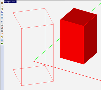
- Once imported, the Huygens source appears in the Project Workspace as a wire-frame box.
- You can open the property dialog of a Huygens source by right clicking on its name in the Navigation Tree and selecting Properties... From this dialog you can change the color of the Huygens source box as well as its location and orientation. You can enter new values for the X, Y, Z Center Coordinates and Rotation Angles of the Huygens box. You can also view the dimensions of the box.
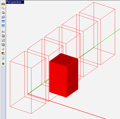
- By default, the Huygens data are imported as a single Huygens source. You can create an arbitrary array of Huygens sources for your PO project. To do so, in the "Create Array" section of the Huygens source dialog, enter desired values for the Number of Elements and Element Spacing along the X, Y and Z directions. You will see an array of wire-frame box appear in the project workspace.
Figure: (Left) A rotated imported Huygens source, and (Right) An array of imported Huygens sources defined to excite a PEC box.
Running PO Simulations
Running A Basic PO Analysis
To open EM.Illumina's Simulation Run dialog, click the Run ![]() button of the Simulate Toolbar or select Menu > Simulate > Run...or use the keyboard shortcut Ctrl+R. To start the simulation click the Run button of this dialog. Once the PO simulation starts, a new dialog called Output Window opens up that reports the various stages of PO simulation, displays the running time and shows the percentage of completion for certain tasks during the PO simulation process. A prompt announces the completion of the PO simulation. At this time, EM.Cube generates a number of output data files that contain all the computed simulation data. These include current distributions, near field data, far field radiation pattern data as well bi-static or mono-static radar cross sections (RCS) if the structure is excited by a plane wave source.
button of the Simulate Toolbar or select Menu > Simulate > Run...or use the keyboard shortcut Ctrl+R. To start the simulation click the Run button of this dialog. Once the PO simulation starts, a new dialog called Output Window opens up that reports the various stages of PO simulation, displays the running time and shows the percentage of completion for certain tasks during the PO simulation process. A prompt announces the completion of the PO simulation. At this time, EM.Cube generates a number of output data files that contain all the computed simulation data. These include current distributions, near field data, far field radiation pattern data as well bi-static or mono-static radar cross sections (RCS) if the structure is excited by a plane wave source.
Setting The Numerical Parameters
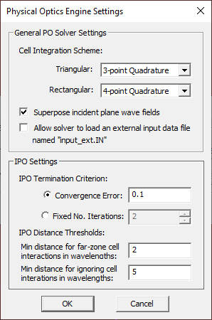
Before you run a PO simulation, you can change some of the PO simulation engine settings. While in the PO Module's Simulation Run Dialog, click the Settings button next to the Select Engine dropdown list. In the Physical Optics Engine Settings Dialog, there are two options for Solver Type: Iterative and GOPO. The default option is Iterative. The GOPO solver is a zero-order PO simulator that uses Geometrical Optics (GO) to determine the lit and shadow cells in the structure's mesh. For the termination of the IPO solver, there are two options: Convergence Error and Maximum Number of Iterations. The default Termination Criterion is based on convergence error, which has a default value of 0.1 and can be changed to any desired accuracy. The convergence error is defined as the L2 norm of the normalized residual error in the combined J/M current solution of the entire discretized structure from one iteration to the next. Note that for this purpose, the magnetic currents are scaled by η0 in the residual error vector.
You can also use higher- or lower-order integration schemes for the calculation of field integrals. EM.Cube's PO simulation engine uses triangular cells for the mesh of the physical surface structures and rectangular cells for discretization of Huygens sources and surfaces. For integration of triangular cells, you have three options: 7-Point Quadrature, 3-Point Quadrature and Constant. For integration of rectangular cells, too, you have three options: 9-Point Quadrature, 4-Point Quadrature and Constant.
PO Sweep Simulations
You can run EM.Illumina's PO simulation engine in the sweep mode, whereby a parameter like frequency, plane wave incident angles or a user defined variable is varied over a specified range at predetermined samples. The output data are saved into data files for visualization and plotting. EM.Illumina currently offers three types of sweep:
- Frequency Sweep
- Angular Sweep
- Parametric Sweep
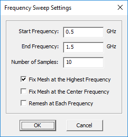
To run a PO sweep, open the Simulation Run Dialog and select one of the above sweep types from the Simulation Mode dropdown list of this dialog. If you select either frequency or angular sweep, the Settings button located next to the simulation mode dropdown list becomes enabled. If you click this button, the Frequency Settings Dialog or Angle Settings Dialog opens up, respectively. In the frequency settings dialog, you can set the start and end frequencies as well as the number of frequency samples. The start and end frequency values are initially set based on the project's center frequency and bandwidth. During a frequency sweep, as the project's frequency changes, so does the wavelength. As a result, the mesh of the structure also changes at each frequency sample. The frequency settings dialog gives you three choices regarding the mesh of the project structure during a frequency sweep:
- Fix mesh at the highest frequency.
- Fix mesh at the center frequency.
- Re-mesh at each frequency.
You can run an angular sweep only if your project has a plane wave excitation. In this case, you have to define a plane wave source with the default settings. During an angular sweep, either the incident theta angle or incident phi angle is varied within the specified range. The other angle remains fixed at the value that is specified in the Plane Wave Dialog. You have to select either Theta or Phi as the Sweep Angle in the Angle Settings Dialog. You also need to set the start and end angles as well as the number of angle samples.
In a parametric sweep, one or more user defined variables are varied at the same time over their specified ranges. This creates a parametric space with the total number of samples equal to the product of the number of samples for each variable. The user defined variables are defined using EM.Cube's Variables Dialog. For a description of EM.Cube variables, please refer to the "Parametric Modeling, Sweep & Optimization" section of EM.Cube Manual or see the "Parametric Sweep" sections of the FDTD or Planar Module manuals.
Working with PO Simualtion Data
EM.Illumina does not produce any output data on its own unless you define one or more observables for your simulation project. The primary output data in the Physical Optics method are the electric and magnetic surface current distributions on the surface of your structure. At the end of a PO simulation, EM.Illumina generates a number of output data files that contain all the computed simulation data. Once the current distributions are known, EM.Illumina can compute near-field distributions as well as far-field quantities such as radiation patterns and radar cross section (RCS). EM.Illumina currently provides the following observables:
- Current Distributions
- Near-Field Distributions
- Far Field - Radiation Patterns
- Far Fields - Radar Cross Section
- Huygens Surface Data
Visualizing Current Distributions
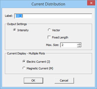
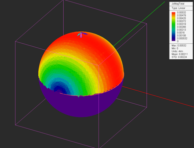
Current distributions are visualized on the surface of the PO mesh cells, and the magnitude and phase of the electric and magnetic surface currents are plotted for all the objects. In order to view these currents, you must first define a current distribution observable before running the PO simulation. A single current distribution node in the navigation tree holds the current distribution data for all the objects in the project workspace. After a PO simulation is completed, new plots are added under the current distribution node. Separate plots are produced for the magnitude and phase of each of the electric and magnetic surface current components (X, Y and Z) as well as the total current magnitude.
The current distributions are plotted on the surface of the individual mesh cells. As a result, some parts of the plots may be blocked by and hidden inside smooth and curved objects. To be able to view those parts, you may have to freeze the obstructing objects or switch to the mesh view mode.
![]() Click here to learn more about Visualizing 3D Current Distribution Maps.
Click here to learn more about Visualizing 3D Current Distribution Maps.
Near-Field Visualization
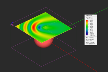
EM.Illumina allows you to visualize the near fields at a specific field sensor plane. Calculation of near fields is a post-processing process and may take a considerable amount of time depending on the resolution that you specify.
![]() Click here to learn more about Defining a Field Sensor Observable.
Click here to learn more about Defining a Field Sensor Observable.
![]() Click here to learn more about Visualizing 3D Near Field Maps.
Click here to learn more about Visualizing 3D Near Field Maps.
Computing Radiation Patterns
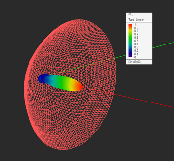
Physical Optics is an open-boundary technique, and you do not need a far field box to perform near-to-far-field transformations. Nonetheless, you still need to define a far field observable if you want to plot radiation patterns. After a PO simulation is finished, three radiation patterns plots are added to the far field node in the Navigation Tree. These are the far field component in θ direction, the far field component in φ direction and the total far field. The 3D plots are displayed in the project workspace and are overlaid on your physical structure.
![]() Click here to learn more about the theory of Far Field Computations.
Click here to learn more about the theory of Far Field Computations.
![]() Click here to learn more about Visualizing 3D Radiation Patterns.
Click here to learn more about Visualizing 3D Radiation Patterns.
![]() Click here to learn more about Plotting 2D Radiation Graphs.
Click here to learn more about Plotting 2D Radiation Graphs.
Computing Radar Cross Section
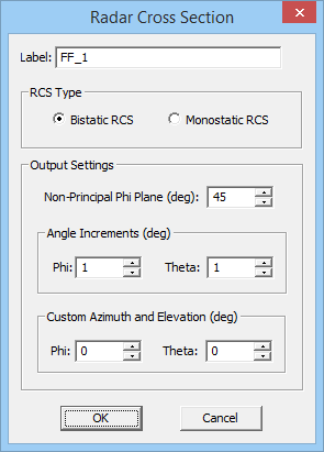
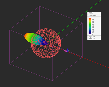
When the physical structure is excited by a plane wave source, the calculated far field data indeed represent the scattered fields. EM.Illumina calculates the radar cross section (RCS) of a target. Three RCS quantities are computed: the θ and φ components of the radar cross section as well as the total radar cross section, which are dented by σθ, σφ, and σtot. In addition, EM.Illumina calculates two types of RCS for each structure: Bi-Static RCS and Mono-Static RCS. In bi-static RCS, the structure is illuminated by a plane wave at incidence angles θ0 and φ0, and the RCS is measured and plotted at all θ and φ angles. In mono-static RCS, the structure is illuminated by a plane wave at incidence angles θ0 and φ0, and the RCS is measured and plotted at the echo angles 180°-θ0; and φ0. It is clear that in the case of mono-static RCS, the PO simulation engine runs an internal angular sweep, whereby the values of the plane wave incidence angles θ and φ are varied over the entire intervals [0°, 180°] and [0°, 360°], respectively, and the backscatter RCS is recorded.
To calculate RCS, first you have to define an RCS observable instead of a radiation pattern. At the end of a PO simulation, the thee RCS plots σθ, σφ, and σtot are added under the far field section of the navigation tree. Keep in mind that computing the 3D mono-static RCS may take an enormous amount of computation time.
![]() Click here to learn more about Visualizing 3D RCS.
Click here to learn more about Visualizing 3D RCS.
![]() Click here to learn more about Plotting 2D RCS Graphs.
Click here to learn more about Plotting 2D RCS Graphs.


