|
|
| Label
|
Host Trace
|
Object Type
|
Function
|
LCS Origin
|
LCS Rotation Angles
|
Outer Radius
|
Inner Radius
|
Start Angle
|
End Angle
|
| Circle_Strip_1
|
PEC_2
|
Circle Strip
|
Wilkinson Power Divider 1
|
(-17mm, 0, 0)
|
(0°, 0°, 0°)
|
9.65mm
|
8.25mm
|
20°
|
340°
|
| Circle_Strip_2
|
PEC_2
|
Circle Strip
|
Wilkinson Power Divider 2
|
(10mm, 62.5mm, 0)
|
(0°, 0°, 0°)
|
9.65mm
|
8.25mm
|
20°
|
340°
|
| Circle_Strip_3
|
PEC_2
|
Circle Strip
|
Wilkinson Power Divider 3
|
(10mm, -62.5mm, 0)
|
(0°, 0°, 0°)
|
9.65mm
|
8.25mm
|
20°
|
340°
|
| Circle_Strip_4
|
PEC_2
|
Circle Strip
|
Round Bend Junction
|
(-6.75mm, 61.3mm, 0)
|
(0°, 0°, 0°)
|
2.4mm
|
0mm
|
0°
|
270°
|
| Circle_Strip_5
|
PEC_2
|
Circle Strip
|
Round Bend Junction
|
(-6.75mm, -61.3mm, 0)
|
(0°, 0°, 0°)
|
2.4mm
|
0mm
|
90°
|
360°
|
| Circle_Strip_6
|
PEC_2
|
Circle Strip
|
Round Bend Junction
|
(20.25mm, 92.55mm, 0)
|
(0°, 0°, 0°)
|
2.4mm
|
0mm
|
0°
|
270°
|
| Circle_Strip_7
|
PEC_2
|
Circle Strip
|
Round Bend Junction
|
(20.25mm, -92.55mm, 0)
|
(0°, 0°, 0°)
|
2.4mm
|
0mm
|
90°
|
360°
|
| Circle_Strip_8
|
PEC_2
|
Circle Strip
|
Round Bend Junction
|
(20.25mm, 32.45mm, 0)
|
(0°, 0°, 0°)
|
2.4mm
|
0mm
|
90°
|
360°
|
| Circle_Strip_9
|
PEC_2
|
Circle Strip
|
Round Bend Junction
|
(20.25mm, -32.45mm, 0)
|
(0°, 0°, 0°)
|
2.4mm
|
0mm
|
0°
|
270°
|
Rectangle strip objects are used for microstrip line segments. Draw the following 16 rectangle strip objects, all on PEC_2 trace plane, with the given coordinates and dimensions:
|
|
| Label
|
Host Trace
|
Object Type
|
Function
|
LCS Origin
|
LCS Rotation Angles
|
X Dimension
|
Y Dimension
|
| Rect_Strip_1
|
PEC_2
|
Rectangle Strip
|
50Ω Input Microstrip Feed Line
|
(-38mm, 0, 0)
|
(0°, 0°, 0°)
|
8mm
|
2.4mm
|
| Rect_Strip_2
|
PEC_2
|
Rectangle Strip
|
50Ω Input Line for Wilkinson Power Divider 1
|
(-30mm, 0, 0)
|
(0°, 0°, 0°)
|
8mm
|
2.4mm
|
| Rect_Strip_3
|
PEC_2
|
Rectangle Strip
|
50Ω Output Line for Wilkinson Power Divider 1
|
(-7.95mm, 32.06mm, 0)
|
(0°, 0°, 0°)
|
2.4mm
|
58.48mm
|
| Rect_Strip_4
|
PEC_2
|
Rectangle Strip
|
50Ω Output Line for Wilkinson Power Divider 1
|
(-7.95mm, -32.06mm, 0)
|
(0°, 0°, 0°)
|
2.4mm
|
58.48mm
|
| Rect_Strip_5
|
PEC_2
|
Rectangle Strip
|
50Ω Input Line for Wilkinson Power Divider 2
|
(-2.75mm, 62.5mm, 0)
|
(0°, 0°, 0°)
|
8mm
|
2.4mm
|
| Rect_Strip_6
|
PEC_2
|
Rectangle Strip
|
50Ω Input Line for Wilkinson Power Divider 3
|
(-2.75mm, -62.5mm, 0)
|
(0°, 0°, 0°)
|
8mm
|
2.4mm
|
| Rect_Strip_7
|
PEC_2
|
Rectangle Strip
|
50Ω Output Line for Wilkinson Power Divider 2
|
(19.05mm, 78.935mm, 0)
|
(0°, 0°, 0°)
|
2.4mm
|
27.23mm
|
| Rect_Strip_8
|
PEC_2
|
Rectangle Strip
|
50Ω Output Line for Wilkinson Power Divider 3
|
(19.05mm, -78.935mm, 0)
|
(0°, 0°, 0°)
|
2.4mm
|
27.23mm
|
| Rect_Strip_9
|
PEC_2
|
Rectangle Strip
|
50Ω Output Line for Wilkinson Power Divider 2
|
(19.05mm, 46.065mm, 0)
|
(0°, 0°, 0°)
|
2.4mm
|
27.23mm
|
| Rect_Strip_10
|
PEC_2
|
Rectangle Strip
|
50Ω Output Line for Wilkinson Power Divider 3
|
(19.05mm, -46.065mm, 0)
|
(0°, 0°, 0°)
|
2.4mm
|
27.23mm
|
| Rect_Strip_11
|
PEC_2
|
Rectangle Strip
|
50Ω Slot Feed Line
|
(30.125mm, 93.75mm, 0)
|
(0°, 0°, 0°)
|
19.75mm
|
2.4mm
|
| Rect_Strip_12
|
PEC_2
|
Rectangle Strip
|
50Ω Slot Feed Line
|
(30.125mm, -93.75mm, 0)
|
(0°, 0°, 0°)
|
19.75mm
|
2.4mm
|
| Rect_Strip_13
|
PEC_2
|
Rectangle Strip
|
50Ω Slot Feed Line
|
(30.125mm, 31.25mm, 0)
|
(0°, 0°, 0°)
|
19.75mm
|
2.4mm
|
| Rect_Strip_14
|
PEC_2
|
Rectangle Strip
|
50Ω Slot Feed Line
|
(30.125mm, -31.25mm, 0)
|
(0°, 0°, 0°)
|
19.75mm
|
2.4mm
|
| Rect_Strip_15
|
PEC_2
|
Rectangle Strip
|
Resistor Line for Wilkinson Power Divider 1
|
(-7.95mm, 0, 0)
|
(0°, 0°, 90°)
|
5.64mm
|
1mm
|
| Rect_Strip_16
|
PEC_2
|
Rectangle Strip
|
Resistor Line for Wilkinson Power Divider 2
|
(19.05mm, 62.5mm, 0)
|
(0°, 0°, 90°)
|
5.64mm
|
1mm
|
| Rect_Strip_17
|
PEC_2
|
Rectangle Strip
|
Resistor Line for Wilkinson Power Divider 3
|
(19.05mm, -62.5mm, 0)
|
(0°, 0°, 90°)
|
5.64mm
|
1mm
|
You will use array objects to represent the repetitive pattern of slot-coupled patch radiators. Specifically, you will build three array objects for the patch element on the top PEC_1 trace plane, the coupling slot on the middle ground plane PMC_1, and the microstrip open stub underneath the slot on the bottom trace plane PEC_2. The table below shows the coordinate and dimensions of the primitive or "parent" objects for each of these arrays. First, you have to draw these objects on the respective planes:
|
|
| Label
|
Host Trace
|
Object Type
|
Function
|
LCS Origin
|
LCS Rotation Angles
|
X Dimension
|
Y Dimension
|
| Rect_Strip_18
|
PEC_2
|
Rectangle Strip
|
Microstrip Open Stub
|
(51.5mm, -93.75mm, 0)
|
(0°, 0°, 0°)
|
23mm
|
2.4mm
|
| Rect_Strip_19
|
PMC_1
|
Rectangle Strip
|
Coupling Slot
|
(45mm, -93.75mm, 0.787mm)
|
(0°, 0°, 0°)
|
1.5mm
|
12mm
|
| Rect_Strip_20
|
PEC_1
|
Rectangle Strip
|
Radiating Patch
|
(45mm, -93.75mm, 2.787mm)
|
(0°, 0°, 0°)
|
31.6mm
|
31.6mm
|
Now, select each of the above primitive objects and use EM.Cube's Array Tool to create a 1×4 Y-directed linear array of that object on the proper plane. Make sure that right trace group on the Navigation Tree is activated before creation of each array object. Use the table below for element count and spacing along the three principal directions.
 |
Once you create an array object, the array's local coordinate system (LCS) takes over the parent object's LCS. The array's LCS rotation angles are independent of the parent object's rotation angles.
|
|
|
| Label
|
Host Trace
|
Primitive Object
|
Array LCS Origin
|
Array LCS Rotation Angles
|
X Count
|
Y Count
|
Z Count
|
X Spacing
|
Y Spacing
|
Z Spacing
|
| Rect_Strip_18
|
PEC_2
|
Rect_Strip_18
|
(51.5mm, -93.75mm, 0)
|
(0°, 0°, 0°)
|
1
|
4
|
1
|
0
|
62.5mm
|
0
|
| Rect_Strip_19
|
PMC_1
|
Rect_Strip_19
|
(45mm, -93.75mm, 0)
|
(0°, 0°, 0°)
|
1
|
4
|
1
|
0
|
62.5mm
|
0
|
| Rect_Strip_20
|
PEC_1
|
Rect_Strip_20
|
(45mm, -93.75mm, 0)
|
(0°, 0°, 0°)
|
1
|
4
|
1
|
0
|
62.5mm
|
0
|
 The geometry of the 4-element slot-coupled patch antenna array with a corporate feed network. |
Next, define three lumped elements of "Resistor" type with a 100Ω value and place them in the middle of the line segments Rect_Strip_15, Rect_Strip_16 and Rect_Strip_17. Also define a default +X-directed de-embedded source on the line object Rect_Strip_1 and assign a default Port Definition observable to it. Define three Current Distribution observables for the PEC_1, PEC_2 and PMC_1 traces. Define a Far Fields Radiation Pattern observable with a 3° Angle Increment for both Theta and Phi, and check its Front-to-Back Ratio (FBR) checkbox. Your antenna array is complete at this point.
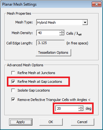 The Planar MoM Mesh Settings dialog. Examining the Mesh of the Planar Array
Similar to Tutorial Lessons 7 and 8, set the mesh density to 40 cells per effective wavelength. Open the Mesh Settings dialog and increase the minimum angle of defective triangular cells to 20°. Also, check the checkbox labeled " Refine Mesh at Gap Locations". This is due to the presence of three lumped elements on very narrow line objects. In EM.Cube's Planar Module, lumped elements behave very similar to gap sources.
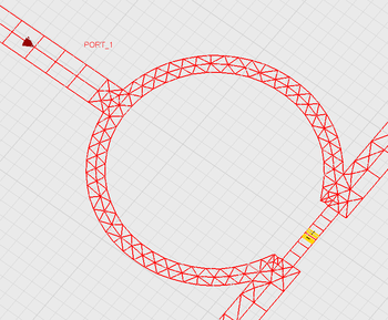
Generate and view the planar MoM mesh of your array structure on all three PEC_1, PMC_1 and PEC_2 planes. The mesh of the corporate feed network is the most complicated one and requires special attention. In particular, closely inspect the mesh at the junctions of microstrip line segments with the Wilkinson circular rings and the around the round corner bend junctions. Also examine the connections to the open stub array. Connections to array objects might sometime be tricky in complicated configurations.
| |
If your planar structure involves a large number of interconnected objects, individual objects with curved shapes, many overlap regions and several gap sources or lumped elements, EM.Cube's mesh generator may fail with low mesh density values. You may be asked to increase the mesh density.
|
 The Planar MoM mesh of the 4-element slot-coupled patch antenna array with a corporate feed network. |
 Details of the planar mesh around the Wilkinson power divider. |
 Details of the planar mesh around the round corner bend junctions. |
Running a Planar MoM Analysis of the Antenna Array
Run a quick planar MoM analysis of your slot-couple patch array structure. The size of the linear system in this case is N = 3,546. At the end of the simulation, the following port characteristic values are reported in the Output Message Window:
S11: -0.197431 - 0.916521j
S11(dB): -0.560162
Z11: 2.660904 - 40.306972j
Y11: 0.001631 + 0.024702j
Note that input match of the array has been seriously degraded compared to that of the single slot-coupled patch antenna you built in Tutorial Lesson 8. Visualize all three current distributions on the PEC_1, PEC_2 and PMC_1 trace planes. You may have to change the limits of the current plot for the feed network due to the presence of a few very hot spots around the line discontinuities.
 The surface electric current distribution on the microstrip feed network of the array after limiting the plot values to 99% confidence interval. |
 The surface electric current distribution on the top patches of the array. |
 The surface magnetic current distribution on the coupling slots of the array. |
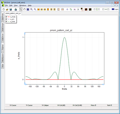
Also visualize the 3D radiation pattern of your patch antenna array and plot the 2D Cartesian and polar graphs in EM.Grid. Note the portion of the radiation pattern in the lower half-space (90° ≤ θ ≤ 180°). This is due to the radiation from the feed network. Open the Data Manager and view the contents of the data file "FBR.DAT". You will see a value of 2.304221e-002 for the front-to-back ratio of the slot-coupled patch array. But it important to note that the computed FBR value is ratio of the total far field value at θ = 180° to the total far field value at θ = 0°. A close inspection of the patterns in the lower half-space reveals that the back lobes peak at θ = 130°, not at θ = 180°. The directivity of the antenna array is found to be 11.15 (or 10.47dB).
 The 3D radiation pattern of the slot-coupled patch antenna array with a corporate feed network. |
 The 2D Cartesian graph of the YZ-plane radiation pattern of the slot-coupled patch antenna array. |
 The 2D Cartesian graph of the ZX-plane radiation pattern of the slot-coupled patch antenna array. |
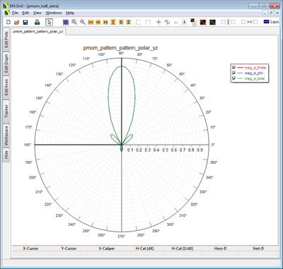
 The 2D polar graph of the YZ-plane radiation pattern of the slot-coupled patch antenna array. |
 The 2D polar graph of the ZX-plane radiation pattern of the slot-coupled patch antenna array. |
 The 3D radiation pattern of a single stand-alone slot-coupled patch antenna multiplied by a 4×1 array factor. Comparison with Array Factor Method
In Tutorial Lesson 8, you could have defined a linear array factor in the Radiation Pattern dialog of the slot-couple patch antenna. Had you done that, the computed radiation pattern would have corresponded to an array of slot-coupled patch antennas rather than the single stand-alone radiator appearing your project workspace. However, the array pattern computed in this manner does not account for the inter-element coupling effects. The figures below have been obtained by multiplying the radiation pattern of the single slot-coupled patch antenna by a 1×4 Y-directed array factor with an element spacing of 62.5mm. The directivity of the array is calculated to be 12.15 (or 10.89dB), which is fairly close to the directivity of the array with the corporate feed network. Comparing the two sets of radiation pattern plots, you can see that even the side lobe and nulls are very similar in both cases. The main difference, however, is in the back lobe characteristics.
 The 2D Cartesian graph of the YZ-plane radiation pattern of a single stand-alone slot-coupled patch antenna multiplied by a 4×1 array factor. |
 The 2D Cartesian graph of the ZX-plane radiation pattern of a single stand-alone slot-coupled patch antenna multiplied by a 4×1 array factor. |
 The 2D polar graph of the YZ-plane radiation pattern of a single stand-alone slot-coupled patch antenna multiplied by a 4×1 array factor. |
 The 2D polar graph of the ZX-plane radiation pattern of a single stand-alone slot-coupled patch antenna multiplied by a 4×1 array factor. |
Back to EM.Cube Wiki Main Page
|
|
|
|


