Analyzing Circuits Using Predefined Tests
![]() Back to RF.Spice A/D Wiki Gateway
Back to RF.Spice A/D Wiki Gateway
Contents
An Overview of RF.Spice A/D Tests
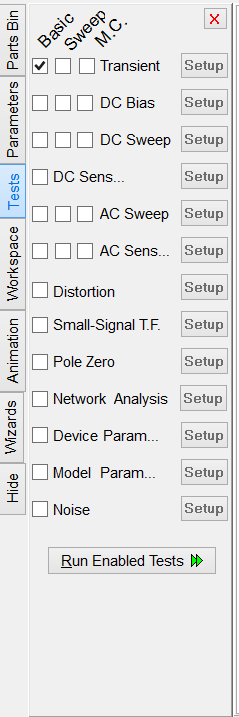
This section describes the details of the various test types available in RF.Spice A/D. You can specify one or more tests to be performed at the same time. This is done using the checkboxes available for each test type in the "Test Panel" of the Toolbox. Most tests offer three options: Basic, Sweep and Monte Carlo (M.C.). The "Basic" test is a single-run simulation, while in a "Sweep" you vary the value of a device parameter. The "Monte Carlo" simulation provides an opportunity to examine the statistical behavior of your circuit given the tolerances for some part values.
In order to run a successful test, you must set up your circuit and specify the relevant simulation parameters correctly. For example, to run an AC sweep test, or a distortion test or a network analysis, you need to specify one or more AC sources in your circuit. Or if you run a transient test of a circuit with DC sources only, you will get the same response over time unless your circuit is an oscillator. You can access and specify the simulation parameters of each test type by clicking the corresponding "Setup" button to open the respective Test Settings dialog.
The output simulation data of a RF.Spice A/D test are presented and displayed either as a graph or in the form of a table. This is done in the "Output Results Options" section of each Test Settings dialog. Note that most tests do not have a default output. You have to specify whether you want a graph or a table or both. Moreover, you have to specify all the voltage or current signals that you want to be plotted or tabulated unless you have defined voltage or current probes in your circuit.
From the Toolbox's Tests tab, you can select, set up, and control any number of tests that can be performed on your circuit. To select a Test and to set it up, click on the "Tests" tab in the Toolbox. The Test Panel shows a list of the available tests with respective checkboxes. Click the "Setup" button next to each test type to set its properties and various available options and settings. Click the green "Run Enabled Tests" button to start the test(s). To learn more about individual tests, please see the section on Tests.
At the bottom of the test panel are three tabs that allow you to run different variations of the selected test. The first tab, Single Test, is a single run through the selected test type using the specified test setup parameters. A graph, table or both can be specified to display the test results. The "Preset Plots" button will allow the specification of plots to display before the test is run. Otherwise, Workshop will automatically plot any meter signals as well as signals specified by the use of Markers.
The Sweep tab allows sweeping of multiple parameters over the test range. For instance, a resistor’s resistance can be stepped from 1K to 10K, with increments by 1K, over the range of a Transient Test. This will actually run 10 Test runs, with the first run having the resistor’s value at 1K, the second will run with the resistor’s value at 2K, and so on, until the resistor’s value is 10K. You can do multilevel sweeps by specifying more than one parameter to sweep, but care must be used, as this will exponentially increase the number of test runs. The Sweep setup button brings up a box that allows you to specify which parameters and how they are swept. The table format is similar to the Live Circuit panel. Select a parameter to sweep and click the Setup Sweep Parameter to set up the sweep parameters. The Monte Carlo Test is similar to the Sweep tests, but the parameter values are varied at random, limited to a user-specified range. The Monte Carlo Setup specifies which parameter to vary and how to randomly vary it.
Transient Test
The transient analysis generates the circuit's behavior as a function of time from tstart to tstop at increments equal to tstep. The maximum interval between time steps, tmax or "Step Ceiling", is critical to prevent the simulation from generating incorrect results. If tmax is too large, then sharp changes in the circuit's voltages may be overlooked by the simulator. RF.Spice A/D gives you the option to linearize your time-domain simulation results, which will generate a second transient graph, with results linearly interpolated at an interval of tstep. The Transient Test is similar to the default "Live Simulation", but the time span is rather finite and it is defined and confined by you. Moreover, the simulation results are displayed in a graph instead of virtual instruments.
The default results of a transient test consist of plots of the voltage across each voltmeter in the circuit and the current through each ammeter as a function of time. You can customize the results by choosing any node voltage or device current using "Preset Graph Plots" and "Preset Table Plots". To learn how you can define output voltages or currents anywhere in your circuit, refer to the section on "Setting Up Circuit Observables". You may also place a voltage probe or a current probe in your circuit to plot its signal as a function of time. To learn more about probes, see the section on "Using Probes or Meters as Observables".
Sometimes the SPICE engine has trouble converging on solutions in a transient analysis. If this happens, increasing capacitances and internal transistor capacitances specified in the transistor models can sometimes relax the circuit enough to help convergence. Also, increasing the value of the "ITL4" parameter in the Simulation Options dialog from its default of 10 to around 40 can sometimes help the solution's convergence. The ITL4 parameter specifies the maximum number of iterations in a transient simulation.
As an example, the figure below shows an Op-Amp circuit (inverting amplifier) with a capacitive load. The graph next to it shows the time-domain input and output voltages of the Op-Amp circuit.
Fourier Analysis of Time-Domain Simulation Data
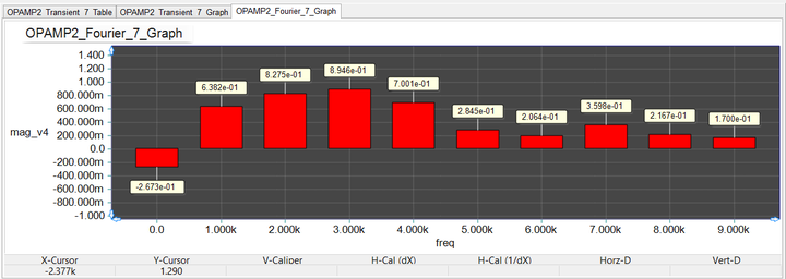
RF.Spice A/D can perform a discrete Fourier transform on the time-domain data at the end of a transient test. The Fourier data represent the spectral contents of the selected signal at a fundamental frequency and its harmonics. To calculate the Fourier transform, check the box titled "Apply Fourier" in the Transient Test's Settings dialog. Then, click the "Fourier Setup" button to open the "Fourier Transform Settings" dialog. In this dialog you can specify the "Fundamental Frequency" in Hertz. You should also indicate which voltage signal must be transformed. For that purpose, either specify the "Output Probe" from a drop-down list of voltage probes in your schematic or specify the "Output Nodes".
As an example, the figure below shows the Fourier contents of the output voltage of the Op-Amp circuit shown earlier. The results of Fourier analysis are plotted in a bar chart representing the spectral contents at the fundamental frequency and its harmonics.
DC Test Types
DC Bias Test
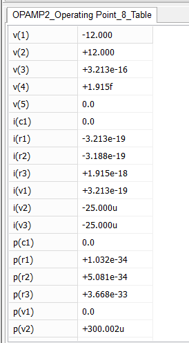
The DC Bias Test, also known as the Operating Point Analysis, calculates all the node voltages and branch currents at the steady (quiescent) state of your circuit. In its most common form, the input can be a constant voltage source or a constant current source. During a DC Bias Test, all capacitors are opened, all inductors are shorted, and all voltage and current sources except for the input source are set to their initial values.
At the end of a DC Bias Test, B2.Spice displays the voltages across voltmeters and the currents through ammeters. The results also appear in tabulated format in a table window at the bottom of your screen. If you enable B2.Spice's Circuit Animation feature, the node voltages and wire currents will be displayed as text or graphically as wire colors on the schematic.
DC Sweep Test
A DC Sweep Test is a set of DC Bias Tests performed successively, during which the value of a parameter (called the sweep variable) is varied. At the end of the simulation, a set of data are generated that correspond to your circuit's response to the different values of the sweep variable. Unlike the DC Bias Test, you must specify the parameters of the DC Sweep Test before you can execute it. At the top of the Settings Dialog, there are two dropdown lists labeled "Source" and "Property". The source can be the name of a constant voltage or current source. The property can be the source's "DC" value. The "Start Value", "End Value" and "Step Value" specify the range and intervals for the source. The analysis starts at the start value, stops at the end value, and increments at intervals equal to the step value. Besides the source voltage or current, the sweep variable can also be a temperature or a device parameter or a model parameter. The input is swept through a set of values, and for each value the DC operating point of the circuit is calculated. That is, all capacitors are opened, all are inductors shorted, and all voltage and current sources except for the input source are set to their initial values. If you want a temperature sweep, the source must be specified as "temperature".
The default results of a DC sweep test consist of plots of the voltage across each voltmeter and the current through each ammeter in the circuit. You can customize the results by choosing any node voltage or device current using "Preset Graph Plots" and "Preset Table Plots". To learn how you can define output voltages or currents anywhere in your circuit, refer to the section on "Setting Up Circuit Observables". You may also place a voltage probe or a current probe in your circuit to plot its signal as a function of the sweep variable. To learn more about probes, see the section on "Using Probes or Meters as Observables".
| /tr> |
Generating Characteristic v-i Curves for Active Devices
The most obvious sweep variable for a DC sweep test is the strength of your source, which can be either the input voltage or input current. This type of analysis is often used to generate the characteristic v-i curves of an active device like a BJT or MOSFET. To make life a little bit easier, RF.Spice A/D provides eleven template projects for the most commonly used active devices including diodes and transistors. These template project files are located in the "Tests" folder in your B2.Spice installation directory:
| Device Type | Test Project File |
|---|---|
| Diode | TEST_Diode.cpr |
| NPN-Type Bipolar Junction Transistor | TEST_BJT_NPN.cpr |
| PNP-Type Bipolar Junction Transistor | TEST_BJT_PNP.cpr |
| N-Channel Junction Field Effect Transistor | TEST_JFET_N.cpr |
| P-Channel Junction Field Effect Transistor | TEST_JFET_P.cpr |
| N-Channel Depletion-Mode MOSFET Transistor | TEST_MOSFET_DEP_N.cpr |
| P-Channel Depletion-Mode MOSFET Transistor | TEST_MOSFET_DEP_P.cpr |
| N-Channel Enhancement-Mode MOSFET Effect Transistor | TEST_MOSFET_ENH_N.cpr |
| P-Channel Enhancement-Mode MOSFET Effect Transistor | TEST_MOSFET_ENH_P.cpr |
| N-Channel MESFET Transistor | TEST_MESFET_N.cpr |
| P-Channel MESFET Transistor | TEST_MESFET_P.cpr |
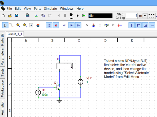
You can readily open any of these projects by going to the Schematic Editor's File Menu and choosing Open > Open Curve Tracer Test Circuit... The standard Windows Open dialog opens up in the "Tests Folder", and you can select and open any of the above eleven test circuits. By default, each test circuit uses a generic active device type. You can easily replace the default generic type with any other model from any manufacturer. Simply select the active device part, go to Schematic Editor's Edit Menu and choose "Edit Part, Device or Model > Select Alternate Model..." This opens up the "Select Model Dialog", where you can search for your new device to the replace the default one.
The supplied test projects already come with all the right test parameters. All you have to do is to press the Run button to run the sweep and generate the characteristic curves. For example, in the case of a BJT, the DC sweep test runs a double sweep of collector-emitter voltage (vce) and the base current (ib). In the test setup panel, the "Source" and "Property" are set to "vce" and "dc", respectively. The value of the base current is another sweep variable set from the Sweep Settings dialog. For more information about sweep tests, please refer to the section on "Parametric Sweeps and Monte Carlo Tests". The figures below show the NPN-type BJT curve tracer test circuit and the graph of its v-i characteristic curves.
DC Sensitivity Test
A DC Sensitivity Test calculates the sensitivity of the output port to all the device values and model parameters at the circuit's operating point. Sensitivity is defined as the derivative an observable like a node voltage with respect to a parameter value such as the resistance of a resistor. In other words, it gives a measure of the variation of the voltage due to a small variation in the value of a part parameter. The output port for sensitivity calculation is specified by a pair of positive and negative (reference) nodes.
| |
In order to view the node numbers in your circuit, check the "Show Node Numbers" option in the View Menu or use the keyboard shortcut "Ctrl+Alt+N". |
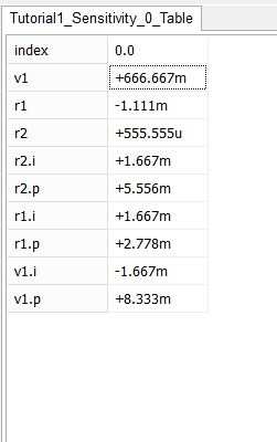
The results of a DC sensitivity test are displayed in a table window. The left column of the table lists the part parameters and the right columns shows the derivative of the output voltage with respect to the respective parameters. For example, consider the simple voltage divider circuit of Tutorial lesson No. 1, which consists of a 1V DC voltage source in series with a 1k resistor and another 2k resistor. The output voltage is designated as the voltage across the 2k resistor. The results of the DC sensitivity test for this circuit indicate that the output voltage is increased by 666.66mV for every 1-volt increase in the input source voltage, it is decreased by -1.111 mV for every 1 Ohm change in the first resistor's value, and it is increased by 555.55 microvolts for every 1 Ohm change in the second resistor's value. Note that these are all small-signal operating point results.
Device Output Parameters Test
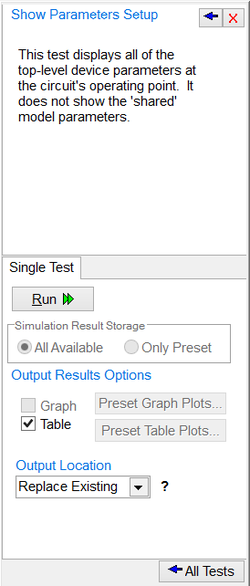
This test shows the operating point details for each of the primitive devices in your circuit. RF.Spice A/D displays the results for all the devices in the circuit in a table window.
Model Output Parameters Test
This test shows the operating point details for each of the process models present in your circuit. RF.Spice A/D displays the results for all the process models present in the circuit in a table window..
AC Test Types
AC Frequency Sweep Test
The AC Frequency Sweep Test is used to examine your circuit's behavior at different input frequencies. For example, a low-pass filter circuit could be analyzed to determine the cut off frequency of the filter, that is, the frequency above which the magnitude of the output is negligible.
| |
Before running an AC analysis, you have to designate one or more AC sources for your circuit and set their AC amplitudes (and phases). During an AC analysis, RF.Spice A/D shorts out all of the non-constant voltage sources that have a zero AC magnitude and opens all the non-constant current sources that have a zero AC magnitude. Make sure that the voltage and current sources used as inputs have non-zero AC voltage/current values. |
All the sources with non-zero AC values are treated as sinusoidal sources with the specified peak voltage/current amplitudes and phases and default zero offsets. You can view or edit the AC values of voltage and current sources by double clicking on the parts and selecting the "Small-Signal AC and Distortion" tab of their property dialog. Make sure to check the "Use" checkbox in the section titled "AC Properties for Small-Signal AC Properties only". Given the specified voltage and current source values, the DC operating point of your circuit is calculated, and all nonlinear elements are replaced with their small-signal circuit models. If the DC operating point of your circuit with the sources shorted out is not where you want it, you may have to place some constant (DC) voltage sources in the circuit to compensate. Alternatively, you can set a nonzero value for the "Small-Signal Offset" parameter of an AC source as shown in the figure below.
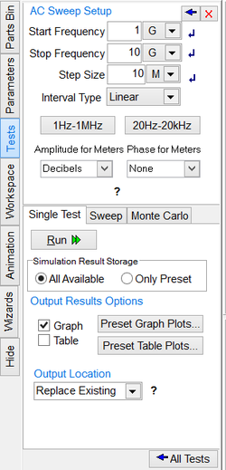
Like the DC analysis, you must specify the parameters of the AC Sweep Test before you can execute it. The Start frequency and Stop frequency specify the range of frequencies for the analysis. The analysis starts at start frequency, stops at stop frequency, and takes place at a number of frequency samples in between. There are three Interval Types: Linear, Decade and Octave. The default scale is "Decade". In a linear scale, you have to specify the "Step Size", which determines the frequency increment. Starting from the Start Frequency, the frequency of the AC source is consecutively incremented by the Step Size until it exceeds the Stop Frequency and the sweep process is terminated. In the case of Decade or Octave interval types, you need to specify the Number of Steps per Interval. A decade is a range from one power of 10 to the next, for example, from 100 to 1000. The points in this case are equally spaced on a log scale. An octave I a range form one power of 2 to the next, for example, from 1 to 2 or from 2 to 4. To actually run the AC analysis, you must click the Run button in the Test Setup for the type of test (Single, Sweep, or Monte Carlo) after specifying the AC Sweep options as described above.
The default results of an AC frequency sweep test consist of plots of the magnitude and phase of the voltage across each voltmeter in the circuit and the magnitude and phase of the current through each ammeter as a function of frequency. The magnitude can be displayed in either decibels or simply magnitude (on a linear scale). A decibel is 20*log10(abs(x)), where x is a real or complex value. For instance, 1000 corresponds to 60 decibels (db), 100 corresponds to 40 db, and 0.1 corresponds to -20db. You can customize the results by choosing any node voltage or device current using "Preset Graph Plots" and "Preset Table Plots". You may also place three types of AC voltage probe: voltage probe (dB), voltage probe (Mag) and voltage probe (Ph-Deg), or three types of AC current probe: current probe (dB), current probe (Mag) and current probe (Ph-Deg) in your circuit to plot their signal as a function of frequency. The default scale used for the plotted graphs at the end of an AC frequency sweep test is base-10-log along the x-axis. If you prefer a linearly scaled frequency axis, change the "Bottom Axis" settings of the graph using the "Edit Axes" tab of the Toolbox in the graph view.
AC Sensitivity Test
The AC Sensitivity Test calculates the small-signal sensitivity of an output port to all device values and model parameters over a range of frequencies. The output port for sensitivity calculation is specified by a pair of positive and negative (reference) nodes. You can also prespecify whether the plots use decibels or magnitude, or degrees or radians.
Distortion Test
The Distortion Test computes the steady-state harmonic products of your nonlinear devices for small-signal inputs. In a distortion analysis, a multidimensional Volterra series analysis is performed using multidimensional Taylor series to represent the nonlinearities at the (DC bias) operating point. Terms of up to the third order are used in the Volterra series expansion. The Distortion test is supported for the following nonlinear devices: diode, BJT, JFET, MOSFET (all levels), MESFET as well as all linear devices. If there are switches present in your circuit, the analysis continues to be accurate provided the switches don not change state under the small-signal excitations used for distortion analysis.
If the input source of your circuit involves a single frequency, the complex values of the second and third harmonics are determined at every point in the circuit. If the input sources of your circuit involve two different frequencies f1 and f2 (f1 > f2), the distortion analysis finds the complex values of the signals at the sum and difference of the input frequencies, i.e. f1+f2 and f1- f2 and at the difference of the smaller frequency from the second harmonic of the larger frequency, i.e. 2*f1 - f2.
| |
In a two-frequency distortion analysis, make sure to set f1 > f2. |
Preparation for a distortion test involves three steps. The first step is similar to the AC Frequency Sweep Test, where you designate one or more AC sources for your circuit and set their AC amplitudes (and phases). Open up the property dialog of all the sources that provide the AC excitation of your circuit. Go to the "Small-Signal AC and Distortion" tab of the property dialog. There are two sections in this tab that pertain distortion analysis. They are titled "Distortion 1 for Distortion Analysis" and "Distortion 2 for Distortion Analysis". The former section is used for a single-frequency distortion test, while either section can be used in a two-frequency distortion analysis. Set the amplitude(s) and phase(s) of the AC signal source and make sure to check the "Use" checkbox in the first or both distortion sections. Phase should be specified in degrees. If phase is missing, it will default to zero.
In the next (second) step, you set up a voltage or current probe or a voltmeter or an ammeter, for which is the harmonic calculations will be performed.
The third and last step of preparation for a distortion test takes place in the Setup Dialog of the Test Panel. In a single-frequency distortion test, the frequency of the designated AC source is swept from the Start Frequency to the Stop Frequency on a linear, decade or octave scale. Similar to the AC Frequency Sweep test, depending on the scale (Interval Type) chosen, you have to set either the Frequency Step or Number of Steps per Interval. For a two-frequency distortion test, you must check the checkbox labeled "Use F2/F1" and then enter a value for the ratio. Note that this ratio must be between 0 and 1. In this case, the analysis considers the circuit with sinusoidal inputs at two different frequencies, F1 and F2. F1 is swept according to the SPICE's DISTO control line options in the input Netlist file. The frequency of the second source F2 is kept fixed at (F2/F1) times the Start Frequency. Each independent source in the circuit may have up to two sinusoidal inputs for distortion at F1 and F2 frequencies. The analysis provides results composed of all node voltages and branch currents at frequencies of F1, F2, F1+F2, F1-F2, and (2*F1)- F2.
Small-Signal Transfer Function Test
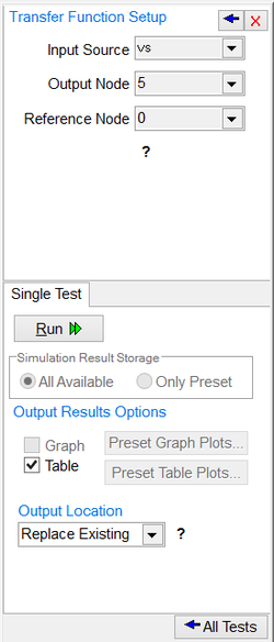
The Transfer Function Test calculates the small-signal transfer function of your circuit by linearizing it around its DC operating point. It generates the input impedance, output impedance and voltage gain seen across your circuit from the input port to the output port. All you need to do is specify the the input source and the output port.
For the simple voltage divider circuit of Tutorial Lesson 1 consisting of two resistors R1 = 1k and R2 = 2k, the transfer function is requested with the output port set between node 2 to ground (across R2), and the voltage source set as the input port. The test results for this example are shown in the opposite figure. The input impedance seen through the voltage source is R1 + R2 = 3k. The output impedance seen from the output port is the parallel combination R1 || R2 = 666.67. The transfer function is V2/V1 = 0.667.
Pole-Zero Test
The Pole-Zero Test generates a list of small-signal poles and zeros of the transfer function of your circuit given the input and output nodes. Specify the input and output ports by the Positive and Negative (Reference) node numbers. To define the transfer function, you have two options: voltage gain by choosing "(output voltage)/(input voltage)" or trans-impedance by choosing "(output voltage)/(input current)". You can instruct the program to compute "Poles Only", or "Zeros Only", or "Pole & Zero".
The results of a Pole-Zero test is displayed as a table. As an example, consider the RLC circuit of Tutorial Lesson 2. Using the voltage gain definition for the transfer function, the Pole-Zero test reports two poles listed below:
| Re(pole(2)) | Imag(pole(2)) | Re(pole(1)) | Imag(pole(1)) |
|---|---|---|---|
| -10.000Meg | -30.000Meg | -10.000Meg | +30.000Meg |
Noise Test
The Noise Test analyzes the device-generated noise over a range of frequencies. For this test you provide an input source, an output port and a range of frequencies. RF.Spice A/D calculates the noise contributions of each device (and each noise generator within each device) to the output port voltage. The program also calculates the equivalent to the output noise referred back to the specified input source. This is what is meant by the "Input Noise". The calculated value of the noise over the specified range of frequencies corresponds to the spectral density of the signal viewed as the square root of a stationary Gaussian stochastic process. After calculating the spectral densities, the simulator integrates these values over the frequency range to arrive at the total noise voltage/current over this frequency range. This calculated value corresponds to the variance of the circuit variable viewed as the square root of a stationary gaussian process.
As for the specific noise sources, they include the "shot" noise associated with the DC currents in semiconductor devices and the "thermal" noise associated with resistance. Semiconductors also display "flicker" (1/f) noise. However, due to the lack of a unified model, RF.Spice A/D handles this type of noise on a "case by case" basis. There are flicker noise parameters available for transistors in the list of model parameters. The program can also provide the noise gain associated with the 1/f source.
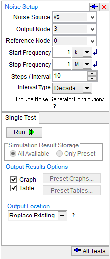
The parameters of the noise test are specified using the setup dialog of the Test Panel. The input noise source can be either a voltage or current source, which you can select from the drop-down list labeled "Noise Source". The output port must be specified as a pair of node numbers, the "Output Node" and the Reference Node". The rest of the parameters specify the frequency interval over which the noise analysis will be performed. They are similar to an AC analysis. If you check the checkbox labeled "Include Noise Generator Contributions", then noise contributions of all the individual devices will be shown as well. If not checked, the input noise and output noise will be shown only.
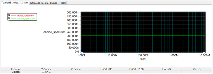
As an example, consider the RTL inverter circuit of Tutorial Lesson 3, which is shown here in the opposite figure. The voltage source Vs is designated as the input noise source. The output port is set at node 3, i.e. the collector of the bipolar junction transistor. The noise is calculated over the frequency range from 1kHz to 10MHz on a decade scale with 10 steps per interval. The figures below show the graph of the noise spectral density over the specified frequency ranges as well as the tabulated results of the noise analysis. The latter are the integrated noise results, representing the total input and output noises as a result of contributions from the discrete devices in the circuit (namely, the resistors and the BJT). The results shown below are the square root of what Berkeley SPICE generates. This is because Berkeley SPICE gives values that are proportional to the noise power rather than the noise voltage.
Nodal Analysis of RF Circuits
The simplest RF circuit analysis type in RF.Spice A/D is the "AC Frequency Sweep" Test. As mentioned earlier, this is identical to the AC frequency sweep test of RF.Spice A/D. The only difference here is that the frequency-domain models of multiport networks and transmission line segments or components are added to the analog or mixed-mode simulation of your circuit. Just as in RF.Spice A/D, the AC Test is run from the Test Panel of the Toolbox.
Defining Sources and Loads
Just as in low frequency circuits, RF circuits must be excited using a voltage or current source. However, in order to ensure a successful RF circuit simulation, your source must be a single-frequency (sinusoidal) AC source. Remember that in RF.Spice A/D circuits, you must specifically designate a source to operate as an AC source for all tests of the AC type. The RF Menu of RF.Spice A/D provides two additional types sources: the AC voltage source with the keyboard shortcut "Alt+V" and the AC current source with the keyboard shortcut "Alt+I". These sources are identical to the regular voltage and current sources of RF.Spice A/D, whose "Use" checkboxes in the AC section of their source property dialog are automatically checked.
| |
For AC-type RF circuit analysis, you can only use AC voltage or current sources with a single common frequency. |
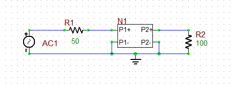
In most RF circuits, the sources are modeled to have an internal source impedance typically denoted by Zs. This source impedance is usually real-valued and typically has a value of 50 Ohms. To model the source impedance, you can simply use a resistor in series with the AC voltage source or a resistor in parallel with the AC current source as shown in the opposite figure. If you need a complex-valued source impedance, you can use a "Complex Impedance" and connected it either in series or in parallel with the AC voltage or current source, respectively.
Similarly, most RF circuits have a load impedance typically denoted by ZL. This load impedance, too, is usually real-valued and typically has a value of 50 Ohms. To model the load impedance, you can simply use a resistor at the output port of your RF circuit. The opposite figure shows a simple RF circuit consisting of a two-port network N1 connected to an AC voltage source with a 50Ω internal resistance and terminated at a 100Ω resistive load. Note how the negative input and output pins of the two-port device have been grounded.
Your load impedance can also be a combination of resistors, capacitors or inductors to model capacitive or inductive loading. Note that in that case you will have a complex-valued load impedance that varies with the operational frequency. In some other cases, you may prefer a user-defined "Complex Impedance" as your load, which cannot be simply modeled as a combination of RLC elements. A resonant antenna load is a good example of this case. The port characteristic data for the antenna structure can be generated by an electromagnetic simulator like EM.Cube and then imported to RF.Spice A/D. If you have the input impedance values as a function of frequency, then you should define a complex impedance load. If you have the return loss (s11) data as a function of frequency (as is usually the case), then you can define a one-port as your load.
Using Transmission Lines for Connecting Parts
You can use Generic T-Line segments or physical transmission line types to connect the various RF parts and devices in your circuit. The opposite figure shows the same simple RF circuit of the previous figure, but containing two T-line segments, one connecting the source to Port 1 of two-port N1 and the other connecting Port 2 of N1 to the resistive load. Note how the negative input and output pins of both T-line segments have been grounded. Lossless transmission line segments cause a phase shift of the propagating signal, while lossy transmission lines also cause additional signal attenuation.
Defining RF Circuit Observables
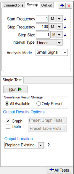
Before you run an AC frequency sweep test of your RF circuit, you need to set the sweep parameters and define the output data for plotting or tabulation. The frequency sweep parameters are set from the test panel of the Toolbox. You set the start and stop frequencies, the frequency interval type (typically linear) and the frequency step. In the lower part of the test panel, you define your simulation output data. Click on the buttons labeled "Preset Graph Plots..." or "Present Table Plots..." to open the Edit Plot List dialog. The dialog gives a list of all the node voltages and currents. You can choose different complex data formats such as Mag/Phase, dB/Phase or Real/Imag.
In the previous RF circuit, the input port has node index 2 and the output port has node index 5. Therefore, the voltage v(2) and v(5) are designated as the simulation output data. The figure below shows a plot of the computed input and output voltages over the frequency range 1-10 GHz. A frequency step size of 10MHz has been set for the frequency sweep.
Network Analysis
RF circuits are typically characterized as multiport networks (usually one-port or two-port). In many practical cases, rather than computing the input or output voltages or currents, you will be more interested in the port characteristics of your RF circuit. The Network Analysis Test characterizes a circuit with one or two ports. It is used to determine the circuit’s behavior as seen through its port(s) and generates data in the form of Z (impedance) parameters, Y (admittance) parameters, S (scattering) parameters, and H parameters. For a one-port circuit, you designate an input port (Port 1) and calculate its return loss or input impedance. For a two-port circuit, you specify an input port (Port 1) and an output port (Port 2) and find its insertion loss or gain. The most commonly used set of parameters for RF circuit characterization are the scattering (S) parameters. The "Network Analysis Test" is one of the AC-type tests of RF.Spice A/D, which computes four sets of parameters: S, Z, Y and H. In the case of a two-port circuit, the four Z parameters are Z11 (the input impedance), Z22 (the output impedance), and Z12 and Z21 (the cross-impedances).
| |
Network analysis is an AC circuit analysis that is typically performed for high frequency circuits. |
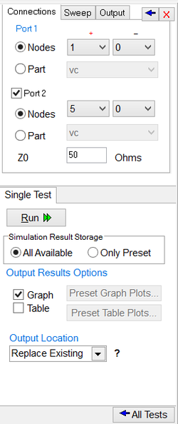
The setup page of Network Analysis has three tabs: Connections, Sweep and Output. All of the parameters in these three tabs must be set carefully to run a successful network analysis test. The "Connections" tab is used to define the input and output ports of your circuit. If only one port of a circuit is being analyzed, then define "Port 1" only. If you have a two-port circuit, then check the checkbox labeled "Port 2" to enable its port definition. The ports can be defined either by their node numbers (positive and negative/reference node indices) or as part names. For example, your input port might be a voltage source. The reference or port characteristic impedance "Z0" is set to 50 Ohms by default. You can change its value if necessary. The "Sweep" tab of setup panel is identical to that of AC Sweep Test. This is where you set up the parameters of your frequency sweep including start and stop frequencies, frequency scale and step. The "Output" tab is used to specify the output data type as well as the graph type. Currently five graph options are available:
- Cartesian (Amplitude)
- Cartesian (Amp/Phase)
- Cartesian (Real/Imag)
- Smith
- Polar
For amplitude graphs, you have the option to plot them in Decibels (dB) scale. For phase graphs, you have the option to express them in degrees. You also need to specify which parameter set to calculate as the output of network analysis. The four options are Z, Y, S or H.
| |
Smith charts and polar graphs are available for S parameters only. |
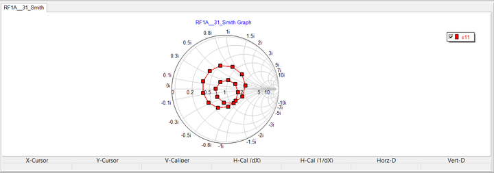
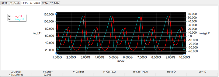
As an example, consider the RF circuit shown earlier for nodal analysis, consisting of a two-port network and connecting transmission line segments. This circuit can be treated as a one-port network with its input port defined between the source's internal resistor and the input T-line segment. As a one-port, the circuit has a single s11 and a single z11 parameter. The first figure below shows the Smith chart for the return loss (s11) over the frequency range 1-10 GHz at larger steps of 100MHz. The second figure below shows Cartesian plots of the real and imaginary parts of z11 over the same frequency range both with finer steps of 10MHz.
