User talk:Asabet
Contents
- 1 FDTD MODULE
- 2 Tutorial Lesson No. 1:
- 3 Analyzing A Center-Fed Resonant Dipole Antenna
- 4 OBJECTIVE:
- 5 YOU WILL LEARN:
- 6 We strongly recommend that you read through the first few tutorials and study them carefully before setting up your own projects.
- 7 1.1 Getting Started
- 8 1.2 FDTD Module Navigation
- 9 1.3 Creating a Wire Object
- 10 1.4 omputational Domain & Boundary Conditions
FDTD MODULE
Tutorial Lesson No. 1:
Analyzing A Center-Fed Resonant Dipole Antenna
OBJECTIVE:
To construct a center‐fed resonant dipole antenna in EM.Cube’s FDTD Module, analyze it and visualize its near and far field characteristics.
YOU WILL LEARN:
A simple half‐wave dipole antenna in free space will be analyzed in the first tutorial. This tutorial will guide you through all necessary steps required to set up and perform a basic FDTD simulation and visualize and graph the simulation results.
We strongly recommend that you read through the first few tutorials and study them carefully before setting up your own projects.
1.1 Getting Started
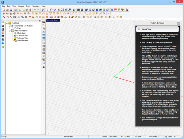
Open the EM.Cube application. Click Start, select All Programs, and then the EMAG program group. Select EM.CUBE to start the program. By default, EM.Cube opens up a blank project with the name “UntitledProj1” in its CubeCAD Module.
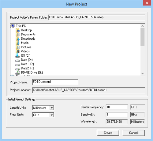
You can start drawing objects and build up your physical structure right away. Or you can initiate a new project by selecting the New button of the System Toolbar (or using the keyboard shortcut Ctrl+N, or via the menu File New Project…). This opens up the New Project Dialog, where you can enter a title for your new project and set its path. You can use the Windows Explorer to go to the desired folder where you want to place your new project folder. For this project, use the title “FDTDLesson1”. From the same dialog, you can also set the project’s Length Units, Frequency Units, Center Frequency and Bandwidth. For this tutorial lesson, set the length and frequency units of the project to Millimeters and Gigahertz, respectively, and set both the center frequency and bandwidth to 1GHz. Then, click the Create button of the dialog to accept the settings. A new project folder with your given name is immediately created at your specified path.
EM.Cube’s CubeCAD Module lets you construct 3D geometries, or import them via external model files such as *.stp, *igs, or *.stl. Once these geometries have been modified or completed, they can be moved to other modules within EM.Cube for further simulation. On the other hand, all modules of EM.Cube offer full CAD operations by themselves. Therefore, you can build a new project from the ground up in any of EM.Cube’s computational modules.
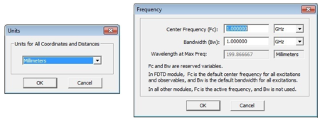
Before you begin to set up the geometry of your project, let’s quickly ensure that the project units are set up correctly. First, open up the Units Dialog box by selecting the Units button of the Simulate Toolbar (or using the keyboard shortcut Ctrl+U). Make sure the length units are Millimeters, and select OK to continue. Similarly, for frequency and bandwidth, select the Frequency button of the Simulate Toolbar (or use the keyboard shortcut Ctrl+F) to open the Frequency Dialog box. Make sure both the frequency and bandwidth are 1GHz, and select OK to continue.
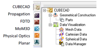
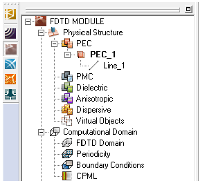
To navigate to FDTD module, simply select its icon from the Module Toolbar on the left side of the screen. Any module may be selected this way. Selecting the module icon changes the Navigation Tree to represent the types of objects supported by the current module. The Navigation Tree of all computational modules features To navigate to FDTD module, simply select its icon from the Module Toolbar on the left side of the screen. Any module may be selected this way. Selecting the module icon changes the Navigation Tree to represent the types of objects supported by the current module. The Navigation Tree of all computational modules features the following nodes: Physical Structure, Computational Domain, Discretization, Sources, and Observables.
The default view in EM.Cube is a 3D Perspective view of the project workspace. A different view can be selected by one of the 7 window selection buttons on the View Toolbar. Further, the 3D window can be split into the Top, Front, Right, and Perspective viewports by clicking on the “Split Viewport” button. This will display four smaller windows simultaneously, allowing you to view your structure from each of these four angles at once. Clicking the “Merge Viewport” button, right next to the “Split Viewport” button, brings the split view back into a single view.
1.3 Creating a Wire Object
Line).
Select the Line Tool from the Object Toolbar (or use the keyboard shortcut F3, or the menu Object Curve
With the line tool selected, click the origin (0,0,0), and drag the mouse to start drawing a line. While still in “Draw Mode”, press and hold the Alt button of the keyboard. This forces the drawn line to be constrained along the alternate Z-axis (normal to the default XY plane on which the mouse pointer moves). Observe the changing Length value in the dialog box as you drag the mouse back and forth. When the length reaches a value of 150 units, left-click to “lock-in” the value. You may also left-click at any point and adjust the length by typing in a value of 150 in the object’s property dialog.
[Image:fdtd_lec1_8_lineproprerties.png|400px]]
Since the center frequency of the project is 1GHz, the operating wavelength is:
For your resonant dipole to be half-wave, it can be approximated at 150mm.
Once your drawing is complete, you can zoom to fit your stucture into the screen using the keyboard shortcut Ctrl+E or by clicking the Zoom Extents button of View Toolbar. After you have rotated or panned the view, you can always restore EM.Cube’s standard perspective view using the keyboard’s Home Key or by clicking the Perspective View button of View Toolbar.
1.4 omputational Domain & Boundary Conditions
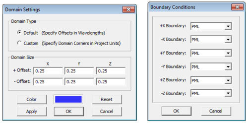
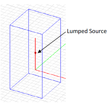
As soon as you draw your first object in FDTD Module’s project workspace, a blue wireframe box appears which completely encloses your object. This is FDTD Module’s computational domain box. Since FDTD is a finite-domain numerical technique, it requires a computational domain of finite extents. By default, the domain box is placed a quarter free space wavelength from the largest bounding box of your physical structure. You can confirm this by opening the Domain Settings Dialog. Click the Domain Settings button of Simulate Toolbar (or select the menu item Compute Computational Domain Domain Settings… or use the keyboard shortcut Ctrl+A) to bring up the domain dialog box. For the default domain type, the domain size is specified in terms of offsets along the ±X, ±Y, and ±Z directions, i.e., the distances between the largest bounding box of the geometry and all the six domain boundaries. The offsets are expressed in free space wavelengths calculated at the highest frequency of the project, which is fmax = f0 + f/2, where f0 is the center frequency of the project and f is the bandwidth.
The boundary Conditions at the six faces of the computational domain can be set by selecting the menu item Simulate Computational Domain Boundary Conditions… or by right clicking on the “Boundary Conditions” item in the “Computational Domain” section of the Navigation Tree. By default, EM.Cube’s FDTD Module assumes an open-boundary physical structure. All the six boundaries default to PML, or Perfectly Matched Layer, which you are going to maintain for this tutorial lesson. But the dropdown lists allow you to also choose PEC, or a Perfect Electric Conducting boundary, or PMC, a Perfect Magnetic Conducting boundary.
