EM.Picasso Tutorial Lesson 6: Analyzing A Periodic Frequency Selective Surface
Contents
- 1 What You Will Learn
- 2 Getting Started
- 3 Defining the Background Substrate Structure
- 4 Drawing the Periodic Unit Cell
- 5 Defining a Plane Wave Source
- 6 Defining Current Distribution & Field Sensor Observables
- 7 Running a Periodic PMOM Analysis of the FSS
- 8 Running an Adaptive frequency Sweep of the FSS
- 9 Illuminating the FSS with an Obliquely Incident Plane Wave Source
What You Will Learn
In this tutorial you will learn how to define a plane wave source. You will use the plane wave source to illuminate a periodic planar structure and compute its reflection and transmission characteristics. You will also learn how to define field sensors to compute and visualize the electric and magnetic field distributions.
![]() Back to EM.Picasso Tutorial Gateway
Back to EM.Picasso Tutorial Gateway
![]() Download projects related to this tutorial lesson
Download projects related to this tutorial lesson
Getting Started
Open the EM.Cube application and switch to EM.Picasso. Start a new project with the following parameters:
In this tutorial lesson, you will model a periodic frequency selective surface (FSS) whose unit cell is made up of simple metal strips on a thick dielectric substrate.
Defining the Background Substrate Structure
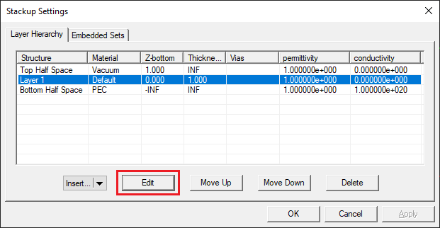
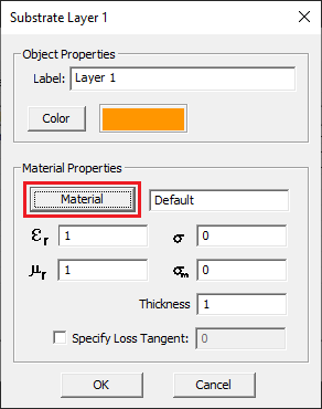
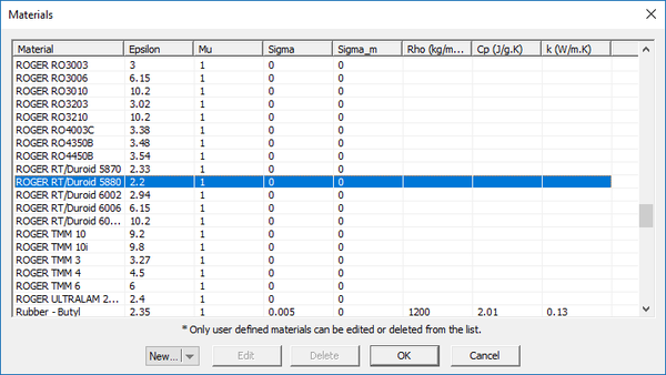
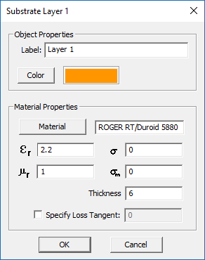
Since you are not going to use a wizard for this project, you have to define the substrate stackup yourself. Open the stackup manager dialog, select and highlight the finite dielectric layer called "Layer 1" and click the Edit button of the dialog. This opens the substrate layer dialog. Click the Material button of this dialog to open EM.Cube's Materials list. Typing the letter "R" on your keyboard takes you to the lower part of the table where the material names start with "R". Select "ROGER RT/Duroid 5880" and click the OK button to return to the substrate layer dialog. You will see the material properties now replaced by those of Duroid.
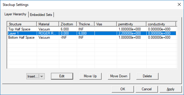
Close the substrate layer dialog and return to stackup manager. In a similar way, change the material composition of the bottom half-space (BHS) to vacuum. The stackup manager should now look like this:
Drawing the Periodic Unit Cell
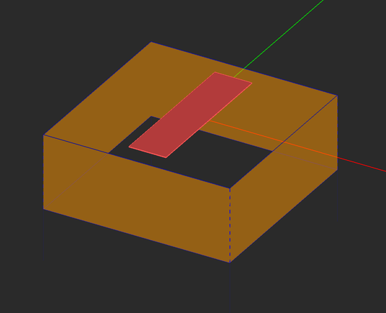
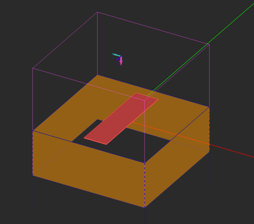
Define a PEC group called PEC_1 and draw a rectangle strip with the following parameters:
| Object | Geometry | Trace Group | Dimensions | LCS Coordinates | Rotation Angles |
|---|---|---|---|---|---|
| RectStrip_1 | Rectangle Strip | PEC_1 | 3mm × 12mm | (0, 0, 6mm) | (0°, 0°, 0°) |
Open EM.Picasso's Periodicity Settings dialog. Check the box labeled Periodic Structure and set the Spacing equal to 15mm along both X and Y directions. Leave the "Offset" boxes with their default zero values. Once you close the periodicity settings dialog and return to the project workspace, you will notice that the domain box has shrunk to the extents of a single unit cell and its side walls are drawn with blue dashed lines.
Defining a Plane Wave Source
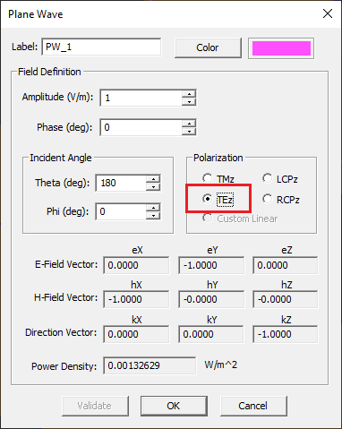
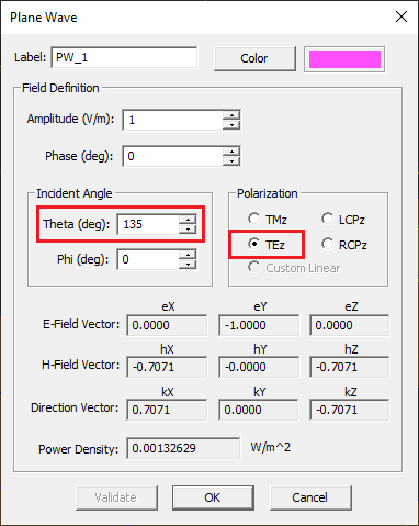
Plane wave sources are used to illuminate and excite periodic surfaces and compute their reflection and transmission characteristics. To define a plane wave source, right-click on the Plane Waves item of the navigation tree and select Insert New Source... from the contextual menu. This opens up the Plane Wave dialog. By default, a downward-looking normally incident plane wave source is assumed. This corresponds to incident Theta and Phi angles of 180° and 0°, respectively. The default polarization of plane wave source is "TMz". For this project. choose TEz as your place wave source's Polarization. Once you close the Plane Wave dialog, a purple box appears around your physical structure with a trident showing the directions of the source's propagation vector, E-field and H-field polarization vectors, in magenta, dark blue, and turquoise, respectively.
| |
In EM.Picasso, the incident angles of a plane wave source correspond to its propagation vector. |
Defining Current Distribution & Field Sensor Observables
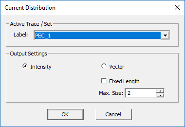
In the previous tutorial lessons, the wizards automatically defined a current distribution observable for your project. Current distribution is the simplest observable in EM.Picasso. Right-click on the Current Distributions item in the “Observables” section of the navigation tree and select Insert New Observable… In the Current Distribution Dialog, select the trace group "PEC_1" from the drop-down list and click OK to close the dialog.
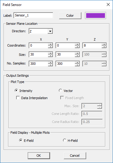
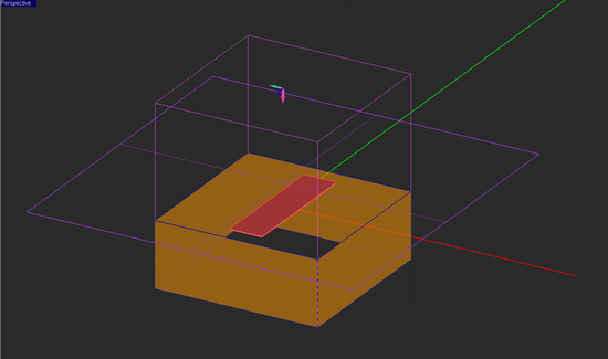
Field sensors are used to compute and visualize the electric and magnetic field distributions on a plane. Right-click on the Near-Field Sensors item of the navigation tree and select Insert New Observable... from the contextual menu. This opens up the Field Sensor dialog. Choose a Z-directed sensor plane from the dropdown list labeled Direction. Set the coordinates to (0, 0, 8mm), which would plane a horizontal plane 2mm above the metallic strip at the top face of the dielectric substrate. Set the dimensions of the field sensor plane to 30mm × 30mm with 300 samples along both X and Y directions.
Running a Periodic PMOM Analysis of the FSS
Set the planar mesh density to 30 cells per effective wavelength. Run a quick single-frequency planar MoM analysis of your periodic planar surface. At the end of the simulation, the computed reflection and transmission coefficients are reported in the output message window.
| Source Case | Polarization | Theta | Phi | Reflection Coefficient | Transmission Coefficient |
|---|---|---|---|---|---|
| 1 | TEz | 180° | 0° | -0.908299 - 0.222347j | -0.344712 - 0.0820254j |
| |
If your structure is periodic and excited by a plane wave source, EM.Picasso always computes its reflection and transmission coefficients without a need to define an observable for it. |
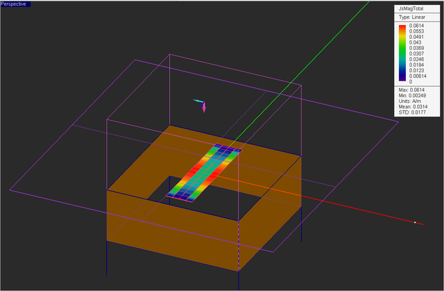
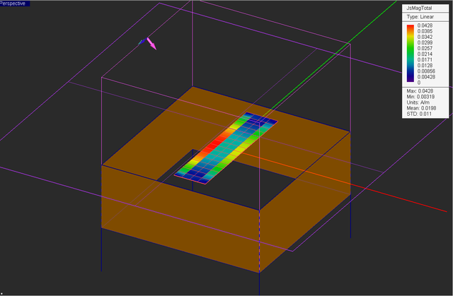
Visualize the current distribution on the surface of the strip (you may need to "Freeze" the Rect_Strip_1).
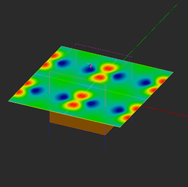
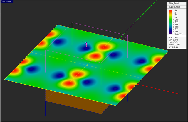
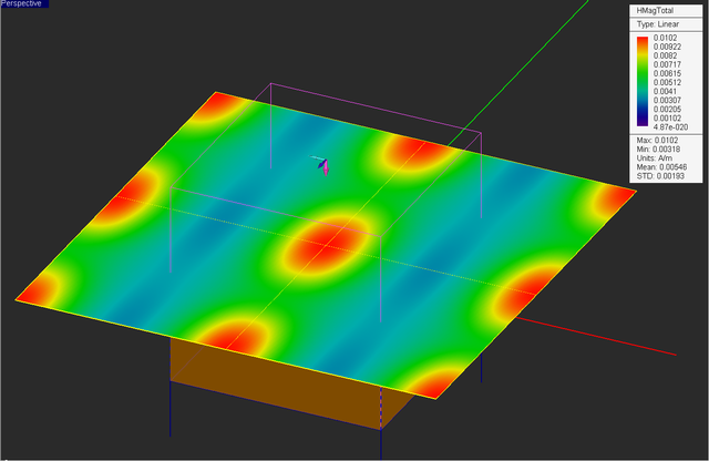
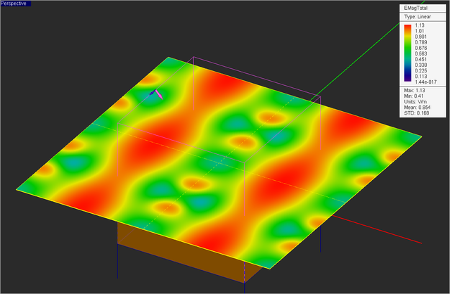
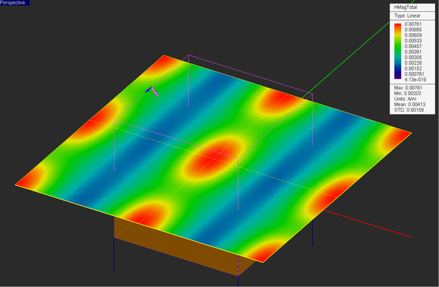
At the end of the simulation a total of 14 plots are added under the field sensor node. These are the magnitude and phase of the sixe field components Ex, Ey, Ez, Hx, Hy, Hz, as well as the total electric field and total magnetic field distributions. Note that the linear dimensions of the sensor plane are twice as large as the unit cell. So you can clearly see the periodic nature of the field distributions from the figures below.
Running an Adaptive frequency Sweep of the FSS
Now let's run a frequency sweep of your periodic surface to examine its frequency response. The reflection and transmission coefficients of a periodic surface are equivalent to the S11 and S21 parameters of a two-port network, where the top and bottom half-spaces serve as Ports 1 and 2, respectively. Run an adaptive frequency sweep with the following parameters:
| Start Frequency | 2GHz |
|---|---|
| End Frequency | 16GHz |
| Min. Number of Frequency Samples | 5 |
| Max. Number of Frequency Samples | 15 |
| Convergence Criterion | 0.02 |
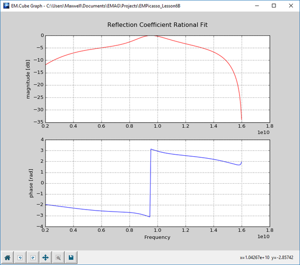
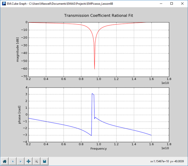
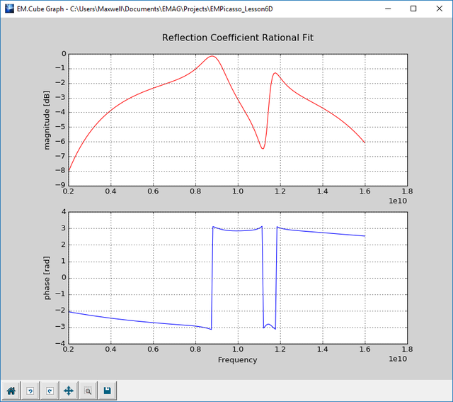
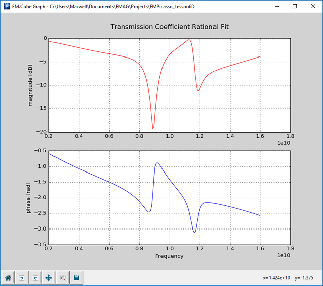
After the completion of the frequency sweep, open the data manager and plot the data files "REFLECTION_RationalFit.CPX" and "TRANSMISSION_RationalFit.CPX". The figures below show the computed reflection and transmission coefficients as a function of frequency for normal plane wave incidence with a TEz polarization.
Illuminating the FSS with an Obliquely Incident Plane Wave Source
Open the property dialog of the plane wave source and change its Theta angle to 135°. In this case you will have an obliquely incident plane wave whose propagation vector makes a 45° angle off the zenith. Run another PMOM analysis and note the new reflection and transmission coefficients.
| Source Case | Polarization | Theta | Phi | Reflection Coefficient | Transmission Coefficient |
|---|---|---|---|---|---|
| 2 | TEz | 135° | 0° | -0.963313 + 0.103053j | 0.0409091 - 0.11252j |
Visualize the current distribution on the strip as well as the total electric and magnetic field distributions on the field sensor plane "Sensor_1".
From the figures below, you can see that magnetic field distribution doesn't change much due to the oblique incidence, but the electric field distribution has a completely different pattern for θ = 135°.
Finally, run an adaptive frequency sweep of your periodic surface with the oblique plane wave incidence. Use the same frequency sweep parameters as in the previous part:
| Start Frequency | 2GHz |
|---|---|
| End Frequency | 16GHz |
| Min. Number of Frequency Samples | 5 |
| Max. Number of Frequency Samples | 15 |
| Convergence Criterion | 0.02 |
At the end of the frequency sweep, plot the data files "REFLECTION_RationalFit.CPX" and "TRANSMISSION_RationalFit.CPX" and note how much the frequency response changes with the angle of incidence.
