Difference between revisions of "EM.Picasso Lesson 5: Modeling Periodic Frequency Selective Surfaces"
Kazem Sabet (Talk | contribs) |
Kazem Sabet (Talk | contribs) |
||
| Line 1: | Line 1: | ||
| − | {{projectinfo|Tutorial| Modeling Periodic Frequency Selective Surfaces| | + | {{projectinfo|Tutorial| Modeling Periodic Frequency Selective Surfaces|PMOM255.png|In this project, you will build and analyze a periodic planar structure illuminated by a plane wave source.| |
*[[CubeCAD]] | *[[CubeCAD]] | ||
*Periodicity | *Periodicity | ||
| Line 61: | Line 61: | ||
[[Image:PMOM252.png|thumb|350px|The geometry of the Wilkinson power divider without the lumped resistor.]] | [[Image:PMOM252.png|thumb|350px|The geometry of the Wilkinson power divider without the lumped resistor.]] | ||
| − | ==Running a Planar MoM Analysis== | + | ==Running a Periodic Planar MoM Analysis== |
Set the planar mesh density to 30 cells per effective wavelength. View and inspect the generated mesh. Also define a default current distribution observable. | Set the planar mesh density to 30 cells per effective wavelength. View and inspect the generated mesh. Also define a default current distribution observable. | ||
| Line 136: | Line 136: | ||
| + | ==Running an Adaptive Frequency Sweep== | ||
| + | In the last part of this tutorial lesson, let's run a frequency sweep of your periodic surface to examine its frequency response. Run an adaptive frequency sweep with the following [[parameters]]: | ||
| − | + | Frequency Sweep Type: Adaptive | |
| − | + | Start Frequency: 2GHz | |
| − | + | End Frequency: 16GHz | |
| − | + | Min No. of Frequency Samples: 5 | |
| − | + | Max No. of Frequency Samples: 15 | |
| − | + | Convergence Criterion: 0.02 | |
| − | |||
| + | Start the adaptive frequency sweep simulation and wait until it convergence. You may get a message asking if you want to continue as the required error criterion was not met within the specified maximum number of samples. Let the program continue until converges successfully. The figure below show the computed reflection and transmission coefficients as a function of frequency for normal plane wave incidence with a TEz polarization. | ||
| − | |||
| − | + | <table> | |
| + | <tr> | ||
| + | <td> | ||
| + | [[Image:PMOM260.png|thumb|400px|Plot of the magnitude and phase of the reflection coefficient of the strip FSS with normal TEz incidence.]] | ||
| + | </td> | ||
| + | <td> | ||
| + | [[Image:PMOM261.png|thumb|400px|Plot of the magnitude and phase of the transmission coefficient of the strip FSS with normal TEz incidence.]] | ||
| + | </td> | ||
| + | </tr> | ||
| + | </table> | ||
| − | |||
| − | |||
| + | <table> | ||
| + | <tr> | ||
| + | <td> | ||
| + | [[Image:PMOM262.png|thumb|400px|Plot of the magnitude and phase of the reflection coefficient of the strip FSS with oblique TEz incidence.]] | ||
| + | </td> | ||
| + | <td> | ||
| + | [[Image:PMOM263.png|thumb|400px|Plot of the magnitude and phase of the transmission coefficient of the strip FSS with oblique TEz incidence.]] | ||
| + | </td> | ||
| + | </tr> | ||
| + | </table> | ||
| − | |||
| − | |||
| − | |||
| − | |||
| − | |||
| − | |||
| − | |||
| − | |||
| − | |||
| − | |||
| − | |||
| − | |||
| − | |||
| − | |||
| − | |||
| − | |||
| − | |||
| − | |||
| − | |||
| − | |||
| − | |||
| − | |||
| − | |||
| − | |||
| − | |||
| − | |||
| − | |||
| − | |||
| − | |||
| − | |||
| − | |||
| − | |||
| − | |||
| − | |||
| − | |||
| − | |||
| − | |||
| − | |||
| − | |||
| − | |||
| − | |||
| − | |||
| − | |||
| − | |||
| − | |||
| − | |||
| − | |||
| − | |||
| − | |||
| − | |||
| − | |||
| − | |||
| − | |||
| − | |||
| − | |||
| − | |||
| − | |||
| − | |||
| − | |||
| − | |||
| − | |||
| − | |||
| − | |||
| − | |||
| − | |||
| − | |||
| − | |||
| − | |||
| − | |||
| − | |||
| − | |||
| − | |||
[[EM.Cube | Back to EM.Cube Wiki Main Page]] | [[EM.Cube | Back to EM.Cube Wiki Main Page]] | ||
Revision as of 19:25, 28 October 2014
Contents
Objective:
To construct a periodic planar structure in EM.Cube’s Planar Module, excite it with a plane wave source and compute its reflection and transmission characteristics.
What You Will Learn:
In this tutorial lesson you will use EM.Cube's spectral domain periodic Planar MoM simulation engine and will learn how to define plane wave sources.
Getting Started
Open the EM.Cube application and switch to Planar Module. Start a new project with the following attributes:
- Name: PMOMLesson5
- Length Units: mm
- Frequency Units: GHz
- Center Frequency: 9GHz
- Bandwidth: 14GHz
- Number of Finite Substrate Layers: 1
- Top Half-Space: Vacuum
- Middle Layer: ROGER RT/Duroid 5880, εr = 2.2, μr = 1, σ = σm = 0, thickness = 6mm
- Bottom Half-Space: Vacuum
Drawing the Periodic Unit Cell
Define a PEC group called PEC_1 and draw a rectangle strip of dimensions 3mm × 12mm. Open the Periodicity Dialog of the Planar Module by right-clicking on the "Periodicity" item of the Navigation Tree and selecting "Periodicity Settings..." from the contextual menu. Check the box labeled "Periodic Structure" and set the "Spacing" equal to 15mm along both X and Y directions. Leave the "Offset" boxes with their default zero values.
Defining a Plane Wave Source
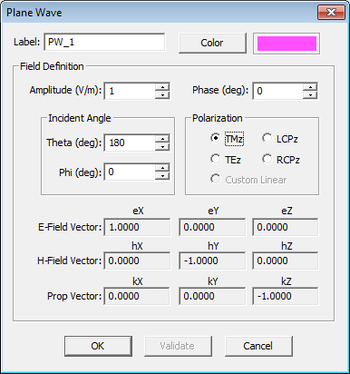
Plane wave source are used to illuminate and excite periodic surfaces and compute their reflection and transmission characteristics. To define a plane wave source, right-click on the "Plane Waves" item of the Navigation Tree and select "Insert New Source..." from the contextual menu. This opens up the Plane Wave Source dialog. By default, a downward-looking normally incident plane wave source is assumed. This corresponds to incident Theta and Phi angles of 180° and 0°, respectively. Also, the default polarization of plane wave source is "TMz". You can also choose "TEz" or circular polarizations RCPz and LCPz.
| |
In EM.Cube, the incident angles of a plane wave source correspond to its propagation vector. |
For this part of the tutorial lesson, you will start with the default plane wave source and then change its polarization as well as its incident Theta and Phi angles.
Running a Periodic Planar MoM Analysis
Set the planar mesh density to 30 cells per effective wavelength. View and inspect the generated mesh. Also define a default current distribution observable.
| |
If your structure is periodic and excited by a plane wave source, EM.Cube always computes its reflection and transmission coefficients without a need to define an observable. |
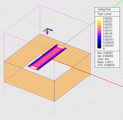
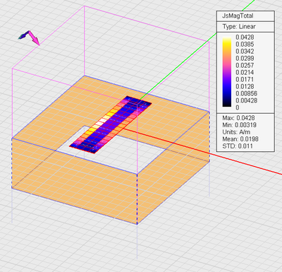
Run a quick planar MoM analysis of your periodic planar surface. At the end of the simulation, read the values of the computed reflection and transmission coefficients in the output message window. Also visualize the current distribution of the surface of the strip. Repeat this procedure for the following combination of source polarization and incident Theta and Phi angles:
Running an Adaptive Frequency SweepIn the last part of this tutorial lesson, let's run a frequency sweep of your periodic surface to examine its frequency response. Run an adaptive frequency sweep with the following parameters: Frequency Sweep Type: Adaptive Start Frequency: 2GHz End Frequency: 16GHz Min No. of Frequency Samples: 5 Max No. of Frequency Samples: 15 Convergence Criterion: 0.02
|


