Difference between revisions of "RF Tutorial Lesson 9: Impedance Matching Using Tuning Stubs"
Kazem Sabet (Talk | contribs) (→Single-Stub Impedance Matching Using a Series Open Stub) |
Kazem Sabet (Talk | contribs) |
||
| (21 intermediate revisions by 2 users not shown) | |||
| Line 1: | Line 1: | ||
{{projectinfo|Tutorial| Impedance Matching Using Tuning Stubs |RF39.png|In this project, you will design and test tuning stubs to match inductive and capacitive loads.| | {{projectinfo|Tutorial| Impedance Matching Using Tuning Stubs |RF39.png|In this project, you will design and test tuning stubs to match inductive and capacitive loads.| | ||
| − | * | + | *Generic Transmission Line |
| − | * | + | *Impedance Matching |
| − | * | + | *Generic Open Stub |
| − | * | + | *Generic Short Stub |
| − | * | + | *Smith Chart |
| − | * | + | *Return Loss |
| − | |All versions|{{download|http://www.emagtech.com/ | + | |All versions|{{download|http://www.emagtech.com/downloads/ProjectRepo/RFLesson9.zip RF Lesson 9}} }} |
| − | + | == What You Will Learn == | |
In this tutorial you will learn impedance matching using tuning stubs of different types and forms. The goal is to match inductive or capacitive loads to a 50Ω line or source. | In this tutorial you will learn impedance matching using tuning stubs of different types and forms. The goal is to match inductive or capacitive loads to a 50Ω line or source. | ||
| Line 25: | Line 25: | ||
</table> | </table> | ||
| − | Tuning stubs are segments of open-ended or short-ended | + | Tuning stubs are segments of open-ended or short-ended transmission lines that are used for distributed impedance matching. Both open and short stubs can be used for impedance matching. From the transmission line theory, we know that open and short stubs have a pure imaginary input impedance. In view of circuit topology, tuning stubs can be connected to the transmission line circuit in series or parallel configurations. In view of circuit complexity, there are single-stub and double-stubs matching network designs. |
<b>Single-Stub Design</b> | <b>Single-Stub Design</b> | ||
| Line 69: | Line 69: | ||
</table> | </table> | ||
| − | == Single-Stub Impedance Matching Using a Series Open Stub== | + | == A Summary of Series Stub Matching Theory == |
| + | |||
| + | The design of the series tuning stub utilized in the previous part is now explained. Let the load admittance be Y<sub>L</sub> = 1 / Z<sub>L</sub> = G<sub>L</sub> + j B<sub>L</sub>. The admittance looking into a T-Line segment of length d terminated by the load Y<sub>L</sub> is given by: | ||
| + | |||
| + | <math>Y_{in} = Y_0 \frac{ \left(G_L + j B_L \right) + jY_0 t}{Y_0 + j \left( G_L + j B_L \right) t}</math> | ||
| + | |||
| + | where t = tan (β d). The impedance at this point can then be written as: | ||
| + | |||
| + | <math>Z_{in} = \frac{1}{Y_{in}} = R_{in} + j X_{in} = \frac {G_L ( 1+ t^2)}{G_L^2+(B_L + Y_0 t)^2} + j \frac {G_L^2 t - (Y_0 - B_L t)(B_L + Y_0 t)}{Y_0 \left[ G_L^2+(B_L + Y_0 t)^2 \right]} </math> | ||
| + | |||
| + | Now we choose the T-Line segment length d such that R<sub>in</sub> = Z<sub>0</sub>. This results in a quadratic equation for t: | ||
| + | |||
| + | <math> Y_0(G_L - Y_0)t^2 -2B_L Y_0 t + (G_L Y_0 t -G_L^2 -B_L^2) = 0 </math> | ||
| + | |||
| + | which can be solved for t. In the special case G<sub>L</sub> = Y<sub>0</sub>, there is one solution t = -B<sub>L</sub> / 2Y<sub>0</sub>. Otherwise, two distinct roots for t are found. Once t is found, the segment length can be calculated by solving t = tan (2π d / λ<sub>g</sub>). | ||
| + | |||
| + | The stub reactance X is chosen such that X = -X<sub>in</sub>. From this condition, you can find the length of the stub depending on whether you use a short or open stub. Recall that the impedance of an open-ended or shorted transmission line segment of length L is given by: | ||
| + | |||
| + | <math> Z_{open} = -jZ_0 cot(\beta L) </math> | ||
| + | |||
| + | and | ||
| + | |||
| + | <math> Z_{short} = jZ_0 tan(\beta L) </math> | ||
| + | |||
| + | Therefore, the equations for the length L<sub>s</sub> of the open stub or short stub are given by: | ||
| + | |||
| + | <math> X_{open} = -Z_0 cot (2\pi L_s / \lambda_g) = -X_{in} </math> | ||
| + | |||
| + | <math> X_{short} = Z_0 tan (2\pi L_s / \lambda_g) = -X_{in} </math> | ||
| + | |||
| + | == Single-Stub Impedance Matching Using a Series Open Stub == | ||
As a first example, you will design a series open stub to match the inductive load you already encountered at the end of Tutorial Lesson 3. The following is a list of parts needed for this part of the tutorial lesson: | As a first example, you will design a series open stub to match the inductive load you already encountered at the end of Tutorial Lesson 3. The following is a list of parts needed for this part of the tutorial lesson: | ||
| Line 89: | Line 119: | ||
! scope="row"| XTL1 | ! scope="row"| XTL1 | ||
| Generic T-Line | | Generic T-Line | ||
| − | | | + | | Z0 = 50, eeff = 1, len = 75 |
|- | |- | ||
! scope="row"| XTL2 | ! scope="row"| XTL2 | ||
| Generic T-Line | | Generic T-Line | ||
| − | | | + | | Z0 = 50, eeff = 1, len = 18 |
|- | |- | ||
| − | ! scope="row"| | + | ! scope="row"| XTLO1 |
| Generic Open Stub | | Generic Open Stub | ||
| − | | | + | | Z0 = 50, eeff = 1, len = 59.55 |
|- | |- | ||
! scope="row"| R1 | ! scope="row"| R1 | ||
| Line 109: | Line 139: | ||
! scope="row"| L1 | ! scope="row"| L1 | ||
| Inductor | | Inductor | ||
| − | | 6. | + | | 6.37n |
|} | |} | ||
| − | Place and connect the parts as shown in the figure below | + | Place and connect the parts as shown in the figure below. You want to design a matching network between the source circuit consisting of the voltage source, source resistor and the 75mm 50Ω T-Line segment and the inductive load of 100 + j80 Ohms at f = 2GHz. When the length of the connecting (spacer) T-Line is chosen to be 18mm and the length of the open stub is chosen to be 59.55mm, the input impedance looking into the combination of the stub and the load to the right becomes 50Ω. |
| + | <table> | ||
| + | <tr> | ||
| + | <td> | ||
| + | [[File:RF29.png|thumb|600px|left|The RF circuit with a single-stub matching network using a series open stub.]] | ||
| + | </td> | ||
| + | </tr> | ||
| + | </table> | ||
| − | + | To verify this, run a network analysis of the circuit with the tuning stub matching network as a one-port. Use Node 2 (at the input of T-Line segment XTL1) as Port 1. Use the [[parameters]] given in the table below: | |
| − | + | ||
| − | + | ||
| − | + | ||
| − | + | ||
| − | + | ||
| − | + | ||
| − | + | ||
{| border="0" | {| border="0" | ||
|- | |- | ||
| − | | valign=" | + | | valign="top"| |
| − | + | ||
| − | + | ||
| − | + | ||
|- | |- | ||
| − | + | {| class="wikitable" | |
| − | + | ||
| − | + | ||
| − | + | ||
| − | {| | + | |
|- | |- | ||
| − | + | ! scope="row"| Start Frequency | |
| − | + | | 1G | |
| − | + | ||
| − | + | ||
|- | |- | ||
| − | + | ! scope="row"| Stop Frequency | |
| − | + | | 3G | |
| − | = | + | |
| − | + | ||
| − | + | ||
| − | + | ||
| − | + | ||
| − | + | ||
| − | + | ||
| − | + | ||
| − | + | ||
| − | + | ||
| − | + | ||
| − | + | ||
| − | + | ||
| − | + | ||
| − | + | ||
| − | + | ||
| − | + | ||
| − | + | ||
| − | + | ||
| − | + | ||
| − | + | ||
| − | + | ||
| − | + | ||
| − | + | ||
| − | + | ||
| − | + | ||
| − | + | ||
| − | + | ||
| − | + | ||
| − | + | ||
| − | + | ||
| − | + | ||
| − | + | ||
| − | + | ||
| − | + | ||
| − | + | ||
| − | + | ||
| − | + | ||
| − | + | ||
| − | + | ||
| − | + | ||
| − | + | ||
|- | |- | ||
| − | + | ! scope="row"| Steps/Interval | |
| − | + | | 10Meg | |
| − | + | ||
| − | + | ||
|- | |- | ||
| − | | | + | ! scope="row"| Interval Type |
| − | + | | Linear | |
| − | + | ||
| − | + | ||
| − | + | ||
|- | |- | ||
| − | + | ! scope="row"| Parameter Set | |
| − | + | | S | |
| − | + | ||
| − | + | ||
|- | |- | ||
| + | ! scope="row"| Graph Type | ||
| + | | Smith or Cartesian (Amplitude Only) with Decibels unchecked | ||
|} | |} | ||
| + | |||
| + | First, plot the S11 data on the Smith chart. You can see from the figure below that at f = 2GHz, the plot passes through the center of the Smith chart. Then, in the Output tab of the Network Analysis Test Panel, choose "Cartesian (Amplitude)" as the graph type with the "Decibels" box unchecked. This will produce a graph of the return loss, i.e. |s11|, as a function of frequency on a Cartesian graph. Again, you can see a quite good impedance match at 2GHz. | ||
| + | |||
| + | <table> | ||
| + | <tr> | ||
| + | <td> | ||
| + | [[File:RF30.png|thumb|750px|Smith chart showing the input reflection coefficient of the transmission line circuit with series open stub.]] | ||
| + | </td> | ||
| + | </tr> | ||
| + | <tr> | ||
| + | <td> | ||
| + | [[File:RF31.png|thumb|750px|The return loss of the transmission line circuit with series open stub plotted on a linear scale.]] | ||
| + | </td> | ||
| + | </tr> | ||
| + | </table> | ||
== A Summary of Shunt Stub Matching Theory == | == A Summary of Shunt Stub Matching Theory == | ||
| Line 227: | Line 216: | ||
<math> B_{short} = -Y_0 cot (2\pi L_s / \lambda_g) = -B_{in} </math> | <math> B_{short} = -Y_0 cot (2\pi L_s / \lambda_g) = -B_{in} </math> | ||
| − | == | + | == Single-Stub Impedance Matching Using a Shunt Short Stub == |
| − | + | The following is a list of parts needed for this part of the tutorial lesson: | |
| − | + | ||
| − | + | ||
| − | + | ||
| − | + | ||
| − | + | ||
{| border="0" | {| border="0" | ||
|- | |- | ||
| − | | valign=" | + | | valign="top"| |
| − | + | ||
| − | + | ||
| − | + | ||
|- | |- | ||
| + | {| class="wikitable" | ||
| + | |- | ||
| + | ! scope="col"| Part Name | ||
| + | ! scope="col"| Part Type | ||
| + | ! scope="col"| Part Value | ||
| + | |- | ||
| + | ! scope="row"| AC1 | ||
| + | | AC Voltage Source | ||
| + | | 1V | ||
| + | |- | ||
| + | ! scope="row"| XTL1 | ||
| + | | Generic T-Line | ||
| + | | Z0 = 50, eeff = 1, len = 75 | ||
| + | |- | ||
| + | ! scope="row"| XTL2 | ||
| + | | Generic T-Line | ||
| + | | Z0 = 50, eeff = 1, len = 16.5 | ||
| + | |- | ||
| + | ! scope="row"| XTLS1 | ||
| + | | Generic Short Stub | ||
| + | | Z0 = 50, eeff = 1, len = 14.25 | ||
| + | |- | ||
| + | ! scope="row"| R1 | ||
| + | | Resistor | ||
| + | | 50 | ||
| + | |- | ||
| + | ! scope="row"| R2 | ||
| + | | Resistor | ||
| + | | 60 | ||
| + | |- | ||
| + | ! scope="row"| C1 | ||
| + | | Inductor | ||
| + | | 0.995p | ||
|} | |} | ||
| − | + | This time, you will design a matching network between the source circuit and the capacitive load of 60 - j80 Ohms at f = 2GHz. Place and connect the parts as shown in the figure below. When the length of the connecting (spacer) T-Line is chosen to be 16.5mm and the length of the short stub is chosen to be 14.25mm, the input impedance looking into the combination of the stub and the load to the right becomes 50Ω. | |
| − | + | ||
| + | <table> | ||
| + | <tr> | ||
| + | <td> | ||
| + | [[File:RF32.png|thumb|600px|The RF circuit with a single-stub matching network using a series open stub.]] | ||
| + | </td> | ||
| + | </tr> | ||
| + | </table> | ||
| + | |||
| + | To verify your matching network, run a network analysis of your circuit with the following [[parameters]]: | ||
| + | |||
{| border="0" | {| border="0" | ||
|- | |- | ||
| − | | valign=" | + | | valign="top"| |
| − | + | ||
| − | + | ||
| − | + | ||
|- | |- | ||
| + | {| class="wikitable" | ||
| + | |- | ||
| + | ! scope="row"| Start Frequency | ||
| + | | 1G | ||
| + | |- | ||
| + | ! scope="row"| Stop Frequency | ||
| + | | 3G | ||
| + | |- | ||
| + | ! scope="row"| Steps/Interval | ||
| + | | 10Meg | ||
| + | |- | ||
| + | ! scope="row"| Interval Type | ||
| + | | Linear | ||
| + | |- | ||
| + | ! scope="row"| Parameter Set | ||
| + | | S | ||
| + | |- | ||
| + | ! scope="row"| Graph Type | ||
| + | | Smith or Cartesian (Amplitude Only) with Decibels unchecked | ||
|} | |} | ||
| + | |||
| + | Plot the Smith chart and graph the variation of the return loss over the frequency range as shown below: | ||
| + | |||
| + | <table> | ||
| + | <tr> | ||
| + | <td> | ||
| + | [[File:RF33.png|thumb|750px|The original RF circuit with an inductive load.]] | ||
| + | </td> | ||
| + | </tr> | ||
| + | <tr> | ||
| + | <td> | ||
| + | [[File:RF34.png|thumb|750px|The RF circuit with a single-stub matching network using a series open stub.]] | ||
| + | </td> | ||
| + | </tr> | ||
| + | </table> | ||
== A Summary of Double Stub Matching Theory == | == A Summary of Double Stub Matching Theory == | ||
| Line 276: | Line 331: | ||
Solving the above equation, you can find B<sub>1</sub> and the length of the first stub. From the equation B<sub>2</sub> = -B<sub>in</sub>, you can determine the length of the second stub. The two stubs can be open, short or mixed. | Solving the above equation, you can find B<sub>1</sub> and the length of the first stub. From the equation B<sub>2</sub> = -B<sub>in</sub>, you can determine the length of the second stub. The two stubs can be open, short or mixed. | ||
| + | == Double-Stub Impedance Matching Using Two Open Stubs == | ||
| + | |||
| + | In the last part of this tutorial lesson, you will explore a double-stub matching network. The following is a list of parts needed for this part of the tutorial lesson: | ||
| + | |||
| + | {| border="0" | ||
| + | |- | ||
| + | | valign="top"| | ||
| + | |- | ||
| + | {| class="wikitable" | ||
| + | |- | ||
| + | ! scope="col"| Part Name | ||
| + | ! scope="col"| Part Type | ||
| + | ! scope="col"| Part Value | ||
| + | |- | ||
| + | ! scope="row"| AC1 | ||
| + | | AC Voltage Source | ||
| + | | 1V | ||
| + | |- | ||
| + | ! scope="row"| XTL1 | ||
| + | | Generic T-Line | ||
| + | | Z0 = 50, eeff = 1, len = 75 | ||
| + | |- | ||
| + | ! scope="row"| XTL2 | ||
| + | | Generic T-Line | ||
| + | | Z0 = 50, eeff = 1, len = 18.75 | ||
| + | |- | ||
| + | ! scope="row"| XTLO1 | ||
| + | | Generic Open Stub | ||
| + | | Z0 = 50, eeff = 1, len = 21.9 | ||
| + | |- | ||
| + | ! scope="row"| XTLO2 | ||
| + | | Generic Open Stub | ||
| + | | Z0 = 50, eeff = 1, len = 30.6 | ||
| + | |- | ||
| + | ! scope="row"| R1 | ||
| + | | Resistor | ||
| + | | 50 | ||
| + | |- | ||
| + | ! scope="row"| R2 | ||
| + | | Resistor | ||
| + | | 60 | ||
| + | |- | ||
| + | ! scope="row"| C1 | ||
| + | | Inductor | ||
| + | | 0.995p | ||
| + | |} | ||
| + | |||
| + | The double-stub matching network is inserted between the source circuit and the capacitive load of 60 - j80 Ohms at f = 2GHz. Place and connect the parts as shown in the figure below. Note that the length of the connecting (spacer) T-Line is chosen to be λ<sub>g</sub>/8 = λ<sub>0</sub>/8 = 18.75mm. When the lengths of the open shunt stubs XTLO1 and XTLO2 are chosen to be 21.9mm and 30.6mm, respectively, the input impedance looking into the combination of the stub and the load to the right becomes 50Ω. | ||
| + | |||
| + | <table> | ||
| + | <tr> | ||
| + | <td> | ||
| + | [[File:RF35.png|thumb|600px|The RF circuit with a double-stub matching network using two shunt open stubs.]] | ||
| + | </td> | ||
| + | </tr> | ||
| + | </table> | ||
| + | |||
| + | To verify your matching network, run a network analysis of your circuit with the following parameters: | ||
| + | |||
| + | {| border="0" | ||
| + | |- | ||
| + | | valign="top"| | ||
| + | |- | ||
| + | {| class="wikitable" | ||
| + | |- | ||
| + | ! scope="row"| Start Frequency | ||
| + | | 1G | ||
| + | |- | ||
| + | ! scope="row"| Stop Frequency | ||
| + | | 3G | ||
| + | |- | ||
| + | ! scope="row"| Steps/Interval | ||
| + | | 10Meg | ||
| + | |- | ||
| + | ! scope="row"| Interval Type | ||
| + | | Linear | ||
| + | |- | ||
| + | ! scope="row"| Parameter Set | ||
| + | | S | ||
| + | |- | ||
| + | ! scope="row"| Graph Type | ||
| + | | Smith or Cartesian (Amplitude Only) with Decibels unchecked | ||
| + | |} | ||
| + | |||
| + | Plot the Smith chart and graph the variation of the return loss over the frequency range as shown below: | ||
| + | |||
| + | <table> | ||
| + | <tr> | ||
| + | <td> | ||
| + | [[File:RF36.png|thumb|750px|left|The original RF circuit with an inductive load.]] | ||
| + | </td> | ||
| + | </tr> | ||
| + | <tr> | ||
| + | <td> | ||
| + | [[File:RF37.png|thumb|750px|left|The RF circuit with a single-stub matching network using a series open stub.]] | ||
| + | </td> | ||
| + | </tr> | ||
| + | </table> | ||
<p> </p> | <p> </p> | ||
| − | [[Image:Back_icon.png|40px]] '''[[RF.Spice_A/D#RF.Spice_A. | + | [[Image:Back_icon.png|40px]] '''[[RF.Spice_A/D#RF.Spice_A.2FD_Tutorials | Back to RF.Spice A/D Tutorial Gateway]]''' |
Latest revision as of 18:21, 8 November 2016
Contents
- 1 What You Will Learn
- 2 Tuning Stubs: An Overview
- 3 A Summary of Series Stub Matching Theory
- 4 Single-Stub Impedance Matching Using a Series Open Stub
- 5 A Summary of Shunt Stub Matching Theory
- 6 Single-Stub Impedance Matching Using a Shunt Short Stub
- 7 A Summary of Double Stub Matching Theory
- 8 Double-Stub Impedance Matching Using Two Open Stubs
What You Will Learn
In this tutorial you will learn impedance matching using tuning stubs of different types and forms. The goal is to match inductive or capacitive loads to a 50Ω line or source.
Tuning Stubs: An Overview
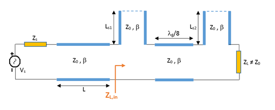
Impedance matching is one of the most important aspects of RF circuit design. The purpose of impedance matching is to connect an arbitrary complex-valued load impedance to a source with a given resistive internal impedance (usually 50Ω) without causing input reflection and to ensure maximum power transfer from the source to the load. In many cases, the given load needs to be impedance-matched to a transmission line of given characteristic impedance as shown in the figure below:
Tuning stubs are segments of open-ended or short-ended transmission lines that are used for distributed impedance matching. Both open and short stubs can be used for impedance matching. From the transmission line theory, we know that open and short stubs have a pure imaginary input impedance. In view of circuit topology, tuning stubs can be connected to the transmission line circuit in series or parallel configurations. In view of circuit complexity, there are single-stub and double-stubs matching network designs.
Single-Stub Design
In a single-stub design, you insert a T-Line segment of length L between the source and load such that the input impedance looking into the T-Line from the point of view of the source has a real part equal to the source resistance. Then you use an open or short stub either in a series or parallel configuration to cancel the imaginary part of the input impedance.
Double-Stub Design
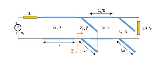
In a double-stub matching network, a tuning stub is placed at the location of the load and another one is placed at a distance of λg/8 from the first stub towards the source. The length of the first stub is chosen such that the combination of the load and first stub moves to the 1+jb circle. The combination load is then rotated along the constant VSWR circle by π/2 towards the source until you intersect the unit r = 1 circle. The length of the second stub is chosen to move you to the center of the Smith chart.
A Summary of Series Stub Matching Theory
The design of the series tuning stub utilized in the previous part is now explained. Let the load admittance be YL = 1 / ZL = GL + j BL. The admittance looking into a T-Line segment of length d terminated by the load YL is given by:
[math]Y_{in} = Y_0 \frac{ \left(G_L + j B_L \right) + jY_0 t}{Y_0 + j \left( G_L + j B_L \right) t}[/math]
where t = tan (β d). The impedance at this point can then be written as:
[math]Z_{in} = \frac{1}{Y_{in}} = R_{in} + j X_{in} = \frac {G_L ( 1+ t^2)}{G_L^2+(B_L + Y_0 t)^2} + j \frac {G_L^2 t - (Y_0 - B_L t)(B_L + Y_0 t)}{Y_0 \left[ G_L^2+(B_L + Y_0 t)^2 \right]} [/math]
Now we choose the T-Line segment length d such that Rin = Z0. This results in a quadratic equation for t:
[math] Y_0(G_L - Y_0)t^2 -2B_L Y_0 t + (G_L Y_0 t -G_L^2 -B_L^2) = 0 [/math]
which can be solved for t. In the special case GL = Y0, there is one solution t = -BL / 2Y0. Otherwise, two distinct roots for t are found. Once t is found, the segment length can be calculated by solving t = tan (2π d / λg).
The stub reactance X is chosen such that X = -Xin. From this condition, you can find the length of the stub depending on whether you use a short or open stub. Recall that the impedance of an open-ended or shorted transmission line segment of length L is given by:
[math] Z_{open} = -jZ_0 cot(\beta L) [/math]
and
[math] Z_{short} = jZ_0 tan(\beta L) [/math]
Therefore, the equations for the length Ls of the open stub or short stub are given by:
[math] X_{open} = -Z_0 cot (2\pi L_s / \lambda_g) = -X_{in} [/math]
[math] X_{short} = Z_0 tan (2\pi L_s / \lambda_g) = -X_{in} [/math]
Single-Stub Impedance Matching Using a Series Open Stub
As a first example, you will design a series open stub to match the inductive load you already encountered at the end of Tutorial Lesson 3. The following is a list of parts needed for this part of the tutorial lesson:
| Part Name | Part Type | Part Value |
|---|---|---|
| AC1 | AC Voltage Source | 1V |
| XTL1 | Generic T-Line | Z0 = 50, eeff = 1, len = 75 |
| XTL2 | Generic T-Line | Z0 = 50, eeff = 1, len = 18 |
| XTLO1 | Generic Open Stub | Z0 = 50, eeff = 1, len = 59.55 |
| R1 | Resistor | 50 |
| R2 | Resistor | 100 |
| L1 | Inductor | 6.37n |
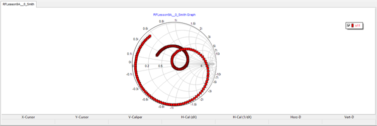
Place and connect the parts as shown in the figure below. You want to design a matching network between the source circuit consisting of the voltage source, source resistor and the 75mm 50Ω T-Line segment and the inductive load of 100 + j80 Ohms at f = 2GHz. When the length of the connecting (spacer) T-Line is chosen to be 18mm and the length of the open stub is chosen to be 59.55mm, the input impedance looking into the combination of the stub and the load to the right becomes 50Ω.
To verify this, run a network analysis of the circuit with the tuning stub matching network as a one-port. Use Node 2 (at the input of T-Line segment XTL1) as Port 1. Use the parameters given in the table below:
| Start Frequency | 1G |
|---|---|
| Stop Frequency | 3G |
| Steps/Interval | 10Meg |
| Interval Type | Linear |
| Parameter Set | S |
| Graph Type | Smith or Cartesian (Amplitude Only) with Decibels unchecked |
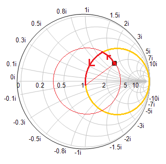
First, plot the S11 data on the Smith chart. You can see from the figure below that at f = 2GHz, the plot passes through the center of the Smith chart. Then, in the Output tab of the Network Analysis Test Panel, choose "Cartesian (Amplitude)" as the graph type with the "Decibels" box unchecked. This will produce a graph of the return loss, i.e. |s11|, as a function of frequency on a Cartesian graph. Again, you can see a quite good impedance match at 2GHz.
A Summary of Shunt Stub Matching Theory
The design of the shunt tuning stub utilized in the previous part is now explained. Let the load impedance be ZL = 1 / YL = RL + j XL. The impedance looking into a T-Line segment of length d terminated by the load ZL is given by:
[math]Z_{in} = Z_0 \frac{ \left(R_L + j X_L \right) + jZ_0 t}{Z_0 + j \left(R_L + j X_L \right) t}[/math]
where t = tan (β d). The admittance at this point can then be written as:
[math]Y_{in} = \frac{1}{Z_{in}} = G_{in} + j B_{in} = \frac {R_L ( 1+ t^2)} {R_L^2+(X_L + Z_0 t)^2} + j \frac {R_L^2 t - (Z_0 - X_L t)(X_L + Z_0 t)} {Z_0 \left[ R_L^2+(X_L + Z_0 t)^2 \right]} [/math]
Now we choose the T-Line segment length d such that Gin = Y0 = 1 / Z0. This results in a quadratic equation for t:
[math] Z_0(R_L - Z_0)t^2 -2X_LZ_0 t + (R_L Z_0 -R_L^2 -X_L^2) = 0 [/math]
which can be solved for t. In the special case RL = Z0, there is one solution t = -XL / 2Z0. Otherwise, two distinct roots for t are found. Once t is found, the segment length can be calculated by solving t = tan (2π d / λg).
The stub susceptance B is chosen such that B = -Bin. From this condition, you can find the length of the stub depending on whether you use a short or open stub. Using the expressions for the impedance of an open-ended or shorted transmission line segment of length L given earlier in this tutorial, the equations for the length Ls of the open stub or short stub are found as:
[math] B_{open} = Y_0 tan (2\pi L_s / \lambda_g) = -B_{in} [/math]
[math] B_{short} = -Y_0 cot (2\pi L_s / \lambda_g) = -B_{in} [/math]
Single-Stub Impedance Matching Using a Shunt Short Stub
The following is a list of parts needed for this part of the tutorial lesson:
| Part Name | Part Type | Part Value |
|---|---|---|
| AC1 | AC Voltage Source | 1V |
| XTL1 | Generic T-Line | Z0 = 50, eeff = 1, len = 75 |
| XTL2 | Generic T-Line | Z0 = 50, eeff = 1, len = 16.5 |
| XTLS1 | Generic Short Stub | Z0 = 50, eeff = 1, len = 14.25 |
| R1 | Resistor | 50 |
| R2 | Resistor | 60 |
| C1 | Inductor | 0.995p |
This time, you will design a matching network between the source circuit and the capacitive load of 60 - j80 Ohms at f = 2GHz. Place and connect the parts as shown in the figure below. When the length of the connecting (spacer) T-Line is chosen to be 16.5mm and the length of the short stub is chosen to be 14.25mm, the input impedance looking into the combination of the stub and the load to the right becomes 50Ω.
To verify your matching network, run a network analysis of your circuit with the following parameters:
| Start Frequency | 1G |
|---|---|
| Stop Frequency | 3G |
| Steps/Interval | 10Meg |
| Interval Type | Linear |
| Parameter Set | S |
| Graph Type | Smith or Cartesian (Amplitude Only) with Decibels unchecked |
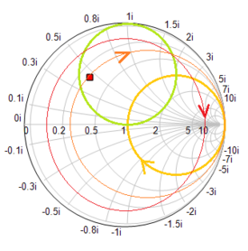
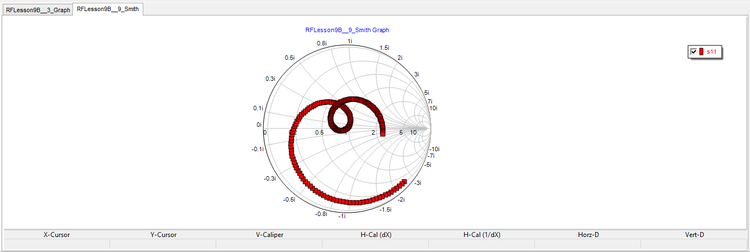
Plot the Smith chart and graph the variation of the return loss over the frequency range as shown below:
A Summary of Double Stub Matching Theory
In this part of the tutorial we scrutinize the design procedure used in the previous part. The first shunt stub is connected in parallel with the load at the load location. Therefore, the total effective load at this point is:
[math]Y_{T} = G_L + j( B_L + B_1) [/math]
where YL = 1 / ZL = GL + j BL is the load admittance and B1 is the susceptance of the first shunt stub. After transforming this admittance through a T-Line segment of length d, the admittance just to the right of the second stub is given by:
[math]Y_{in} = G_{in} + j B_{in} = Y_0 \frac{ G_L + j\left(B_L + B_1 + Y_0 t \right) }{Y_0 + j \left( G_L + j B_L + j B_1 \right) t}[/math]
At this point, to achieve a perfect impedance matching, Gin must equal Y0 and Bin must equal -B2, where B2 is the susceptance of the second shunt stub. This leads to the following equation:
[math] G_L^2 -G_L Y_0 \frac{1+t^2}{t^2} + \frac{ \left( Y_0 -B_L t -B_1 t \right) ^2 } {t^2} = 0 [/math]
Remember that in double stub matching, we fix the distance d between the two shunt stubs. This length is usually chosen to be d = λg/8. In this case, t = tan(β d) = tan(2π d/λg) = tan(π/4) = 1. In this case, the above equation reduces to:
[math] G_L^2 - 2G_L Y_0 + \left( Y_0 -B_L -B_1 \right) ^2 = 0 [/math]
Solving the above equation, you can find B1 and the length of the first stub. From the equation B2 = -Bin, you can determine the length of the second stub. The two stubs can be open, short or mixed.
Double-Stub Impedance Matching Using Two Open Stubs
In the last part of this tutorial lesson, you will explore a double-stub matching network. The following is a list of parts needed for this part of the tutorial lesson:
| Part Name | Part Type | Part Value |
|---|---|---|
| AC1 | AC Voltage Source | 1V |
| XTL1 | Generic T-Line | Z0 = 50, eeff = 1, len = 75 |
| XTL2 | Generic T-Line | Z0 = 50, eeff = 1, len = 18.75 |
| XTLO1 | Generic Open Stub | Z0 = 50, eeff = 1, len = 21.9 |
| XTLO2 | Generic Open Stub | Z0 = 50, eeff = 1, len = 30.6 |
| R1 | Resistor | 50 |
| R2 | Resistor | 60 |
| C1 | Inductor | 0.995p |
The double-stub matching network is inserted between the source circuit and the capacitive load of 60 - j80 Ohms at f = 2GHz. Place and connect the parts as shown in the figure below. Note that the length of the connecting (spacer) T-Line is chosen to be λg/8 = λ0/8 = 18.75mm. When the lengths of the open shunt stubs XTLO1 and XTLO2 are chosen to be 21.9mm and 30.6mm, respectively, the input impedance looking into the combination of the stub and the load to the right becomes 50Ω.
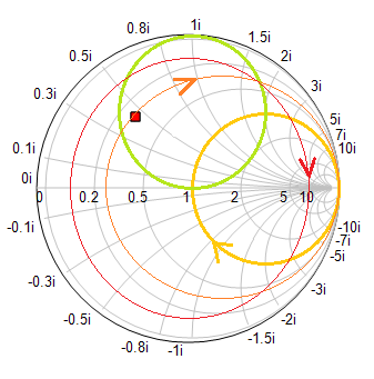
To verify your matching network, run a network analysis of your circuit with the following parameters:
| Start Frequency | 1G |
|---|---|
| Stop Frequency | 3G |
| Steps/Interval | 10Meg |
| Interval Type | Linear |
| Parameter Set | S |
| Graph Type | Smith or Cartesian (Amplitude Only) with Decibels unchecked |
Plot the Smith chart and graph the variation of the return loss over the frequency range as shown below:
