| Tutorial Project: Building Frequency Conversion Mixers With Virtual Blocks
|

|
|
Objective: In this project, you will build and test basic and harmonic mixer systems using black-box virtual blocks.
|
|
Concepts/Features:
- Basic Mixer
- Multiplier Block
- Generic Filter
- Up-Converter Block
- Down-Converter Block
- Frequency Multiplier
- Harmonic Mixer
- Voltage-Controlled Oscillator
|
|
Minimum Version Required: All versions
|
|
' Download Link: System-Level Lesson 5 Download Link: System-Level Lesson 5
|
What You Will Learn
In this tutorial you will learn how to use RF.Spice's spectral processing and frequency conversion black-box virtual blocks such as frequency multipliers, up-converters, down-converters, etc.
Building & Testing a Basic Mixer
The following is a list of parts needed for this part of the tutorial lesson:
|
|
| Part Name
|
Part Type
|
Part Value
|
| VLO
|
Voltage Source
|
Waveform TBD
|
| VIF
|
Voltage Source
|
Waveform TBD
|
| E1 - E2
|
Voltage-Controlled Voltage Source
|
Connections & Dependencies TBD
|
| A1
|
Multiplier Block
|
Defaults
|
| X1
|
Generic Bandpass Filter Block
|
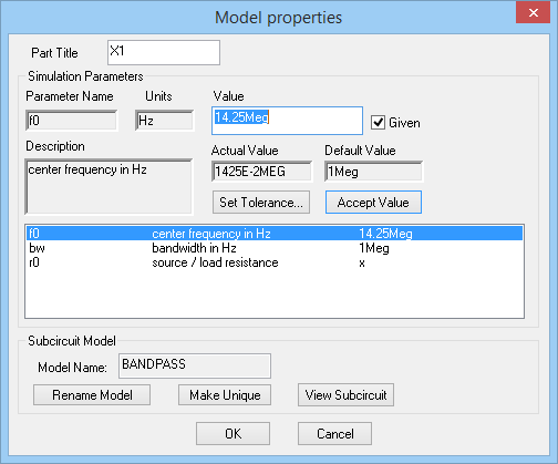
Defaults, Center Frequency = 14.25MHz, Bandwidth = 1MHz
|
| X2
|
Generic Bandpass Filter Block
|
Defaults, Center Frequency = 14.25MHz, Bandwidth = 1MHz
|
| R1 - R3
|
Resistor
|
50
|
In Analog Tutorial Lesson 14, you analyzed a balanced mixer made up of six BJT transistors, an LC tank circuit and three coupling transformers. In other words, you built a physical circuit using real components. In RF.Spice A/D you can also use virtual blocks that accomplish similar functions but without exposing their internal circuit details. In many ways, virtual blocks act like 'Black-Box" parameterized subcircuit models.
A mixer is basically an analog voltage multiplier. When the two inputs of a multiplier, which is a two-signal analog operation block, are two sinusoidal signals with frequencies fLO (local oscillator) and fIF (intermediate frequency), its output will have two frequency components: fRF = fLO ± fIF. You can separate these spectral components using bandpass filters. Once again, you can realize physical filters using L & C components or use virtual blocks as you saw earlier in System-Level Tutorial Lesson 2. In that lesson, you defined a bandpass filter using its mathematical representation, i.e. its s-domain transfer function. RF.Spice's Generic Bandpass Filter Block allows you to simply specify the center frequency and bandwidth of your filter; the rest is taken care of!
 The property dialog of the Generic Bandpass Filter Block. |
Place and connect the parts as shown in the figure below. The two voltage-controlled voltage sources E1 and E2 are used to replicate the output signal of the multiplier block. In other words, both depend on the voltage at Node 3 with a unity gain.
 |
Linear controlled sources can effectively be used to buffer different parts of your circuit or system and replicate various signals without causing undesirable loading effects.
|
 The schematic of the basic mixer circuit. |
Set the waveforms of the two voltage sources VLO and VIF according to the following table:
|
|
VLO: Sinusoid
| Offset Voltage
|
0
|
| Peak Amplitude
|
1V
|
| Frequency
|
12.75MHz
|
| Delay Time
|
0
|
| Damping Factor
|
0
|
|
|
|
VIF: Sinusoid
| Offset Voltage
|
0
|
| Peak Amplitude
|
1V
|
| Frequency
|
1.5MHz
|
| Delay Time
|
0
|
| Damping Factor
|
0
|
Run a Transient Test of this circuit with the parameters specified below:
|
|
| Start Time
|
0
|
| Stop Time
|
15u
|
| Linearize Step
|
1n
|
| Step Ceiling
|
1n
|
| Preset Graph Plots
|
v(1), v(2), v(3), v(5), v(7)
|
The simulation results are shown in the figure below. Once again, you can see that it takes quite a while until the amplitude of the output signals stabilizes.
 The graph of the input and output voltages of the basic mixer circuit. |
Scale the time axis and limit it to the interval t = [14.5μs, 15μs]. The figure below shows the output of the multiplier block along with the outputs of the two bandpass filters. Using the graph window's "Delta Line Mode" try to measure the periods of the filter output signals v(5) and v(7). You will find them to be about 70.2ns and 89ns, respectively, corresponding to the frequency of 14.245MHz and 11.236MHz, as you would have expected.
 The graph of the output signals of the multiplier block and the two bandpass filters in the interval t = [14.5μs, 15μs]. |
Trying Out the Up-Converter and Down-Converter Blocks
The following is a list of parts needed for this part of the tutorial lesson:
|
|
| Part Name
|
Part Type
|
Part Value
|
| VLO
|
Voltage Source
|
Waveform TBD
|
| VIF
|
Voltage Source
|
Waveform TBD
|
| X1
|
Frequency Up-Converter Block
|
Defaults
|
| X2
|
Frequency Down-Converter Block
|
Defaults
|
| R1 - R2
|
Resistor
|
50
|
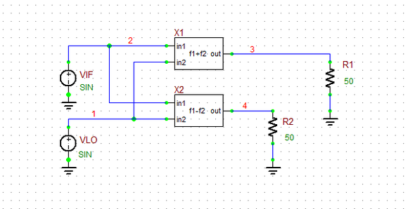
An analog signal multiplier and a bandpass filter together form either a frequency up-converter or a frequency down-converter depending on the passband of the filter. In this part of the tutorial lesson, you will test RF.Spice's up-converter and down-converter blocks. These blocks assume that the two input signals have the same amplitude. Place and connect the parts as shown in the figure below. Note that you don't need buffering controlled source any longer.
 The up-converter and down-converter combo circuit. |
Set the waveforms of the two voltage sources VLO and VIF according to the following table:
|
|
VLO: Sinusoid
| Offset Voltage
|
0
|
| Peak Amplitude
|
1V
|
| Frequency
|
12.75MHz
|
| Delay Time
|
0
|
| Damping Factor
|
0
|
|
|
|
VIF: Sinusoid
| Offset Voltage
|
0
|
| Peak Amplitude
|
1V
|
| Frequency
|
1.5MHz
|
| Delay Time
|
0
|
| Damping Factor
|
0
|
Run a Transient Test of this circuit with the parameters specified below:
|
|
| Start Time
|
0
|
| Stop Time
|
15u
|
| Linearize Step
|
1n
|
| Step Ceiling
|
1n
|
| Preset Graph Plots
|
v(1), v(2), v(3), v(4)
|
The simulation results are shown in the figure below for the the interval t = [14.5μs, 15μs]. You can see that the output signals of this circuit and the circuit of the previous part are almost identical.
 The graph of the input and output voltages of the up-converter and down-converter combo circuit in the interval t = [14.5μs, 15μs]. |
Building & Testing Harmonic Mixers
The following is a list of parts needed for this part of the tutorial lesson:
|
|
| Part Name
|
Part Type
|
Part Value
|
| VLO
|
Voltage Source
|
Waveform TBD
|
| VIF
|
Voltage Source
|
Waveform TBD
|
| A1 - A2
|
Multiplier Block
|
Defaults
|
| X1
|
Frequency Doubler Block
|
Defaults
|
| X2
|
x3 Frequency multiplier Block
|
Defaults
|
| X3
|
Generic Bandpass Filter Block
|
Defaults, Center Frequency = 27MHz, Bandwidth = 0.5MHz
|
| X4
|
Generic Bandpass Filter Block
|
Defaults, Center Frequency = 39.75MHz, Bandwidth = 0.5MHz
|
| R1 - R2
|
Resistor
|
50
|
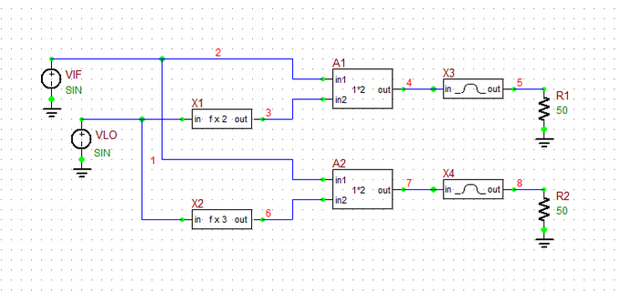
In a harmonic mixer, a harmonic of one input (e.g. LO) is mixed with the other input (e.g. IF) to generate a much higher frequency RF signal. In this project, you will use frequency doubler and frequency tripler virtual blocks to get the second and third harmonics of the LO signal, and will mix them with the IF signal using multiplier blocks. At the output of these block, you will have the frequencies 2*fLO ± fIF and 3*fLO ± fIF. With fLO = 12.75MHz and fIF = 1.5MHz, the output of the first mixer (A1 block) will have 24MHz and 27MHz spectral components, and the output of the second mixer (A2 block) will have 36.75MHz and 39.75MHz spectral components. The lower frequency components are rejected in both mixer using two generic bandpass filter blocks X3 and X4. Set the center frequency of the two filters to 27MHz and 39.75MHz, respectively, and set their bandwidths to 0.5MHz.
Place and connect the parts as shown in the figure below:
 The schematic of the harmonic mixer circuit. |
Set the waveforms of the two voltage sources VLO and VIF according to the following table:
|
|
VLO: Sinusoid
| Offset Voltage
|
0
|
| Peak Amplitude
|
1V
|
| Frequency
|
12.75MHz
|
| Delay Time
|
0
|
| Damping Factor
|
0
|
|
|
|
VIF: Sinusoid
| Offset Voltage
|
0
|
| Peak Amplitude
|
1V
|
| Frequency
|
1.5MHz
|
| Delay Time
|
0
|
| Damping Factor
|
0
|
Run a Transient Test of this circuit with the parameters specified below:
|
|
| Start Time
|
0
|
| Stop Time
|
100u
|
| Linearize Step
|
10n
|
| Step Ceiling
|
10n
|
| Preset Graph Plots
|
v(3), v(5), v(6), v(8)
|
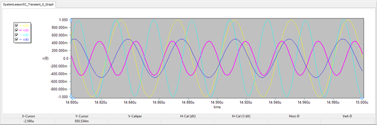
The output voltage graphs are shown in the figures below over a long period of time. v(3) and v(6) are the outputs of the frequency doubler and frequency tripler, respectively. The second figure zooms in the late time period and scales the time axis to t = [14.8μs, 15μs]. The periods of the output voltages v(5) and v(8) are measured to be 37ns and 25.2ns, which correspond to the frequencies 27MHz and 39.7MHz, respectively.
 The graph of the output signals of the frequency doubler and frequency tripler and the two bandpass filters over a long period of time. |
 The graph of the output signals of the frequency doubler and frequency tripler and the two bandpass filters in the interval t = [14.8μs, 15μs]. |
 Back to RF.Spice A/D Tutorial Gateway Back to RF.Spice A/D Tutorial Gateway
|
|
|
|
|
|

