| Tutorial Project: Exploring Phase-Locked Loops
|
|
|
Objective: In this project, you will build simple circuits using RF.Spice's analog phase-locked loop block to verify its frequency and phase locking performance.
|
|
Concepts/Features:
- Analog Phase-Locked Loop
- Phase Detector
- Voltage-Controlled Oscillator
- Loop Filter
- Ideal Phase Shifter
|
|
Minimum Version Required: All versions
|
|
' Download Link: System-Level Lesson 4 Download Link: System-Level Lesson 4
|
What You Will Learn
In this tutorial you will learn how to test and use one of RF.Spice's more complex black-box virtual blocks with a large number of parameters: the analog phase-locked loop (PLL).
Overview of PLL Operation
A phase-locked loop (PLL) is a feedback control system that generates an output signal whose frequency and phase are related to the frequency and phase of an input signal also known as the reference signal. At the heart of a PLL there is a voltage-controlled oscillator (VCO) along with a phase detector. The oscillator initially generates a periodic signal with a certain free-running frequency. The phase detector compares the phase of the VCO signal with the phase of the input periodic signal and adjusts the oscillator to keep the phases matched through the feedback loop. It is clear that keeping the input and output phase in lock step also implies keeping the input and output frequencies the same.
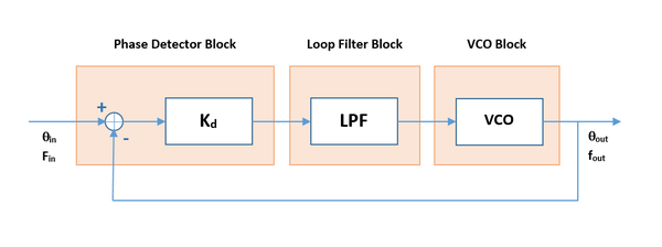 The block diagram of a phase-locked loop system. |
To better understand the operation of the PLL block, consider the highly simplified schematic shown in the figure below. The output of the internal lowpass filter section is directly fed into the input of the internal VCO section, and the output of the VCO section is directly fed back into one of the two inputs of the internal phase detector section. The lowpass filter is a simple RC filter, and you can adjust the values of RLPF and CLPF. The internal VCO section involves a timing RC circuit (integrator), and you can adjust the values of Rtime and Ctime. The nonlinear voltage-controlled source Bpd generates a scaled version of the difference signal (Vin-Vout) with a scaling factor of Kd. The transconductance of the voltage-controlled current source Gvco is equivalent to the conversion gain Kf of the VCO.
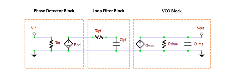 A simplified schematic of the APLL block's internal structure. |
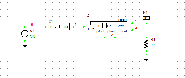
Testing the APLL Device
The following is a list of parts needed for this part of the tutorial lesson:
|
|
| Part Name
|
Part Type
|
Part Value
|
| V1
|
Voltage Source
|
Waveform TBD
|
| A1
|
Analog Phase-Locked Loop (APLL)
|
Defaults
|
| R1
|
Resistor
|
50
|
| IC1
|
Transient Initial Condition Marker
|
1V
|
Place and connect the parts as shown in the Figure below.
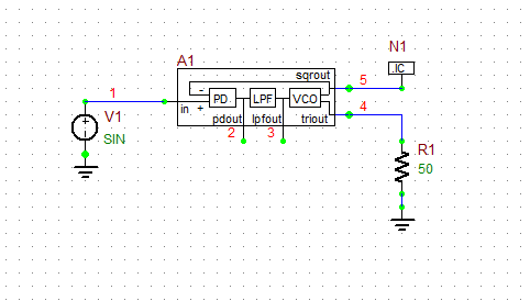 A basic circuit for testing the APLL block. |
You can access the APLL device from Menu > Parts > Spectral Processing Blocks > Phase Locked Loop (PLL) Block. The default free-running frequency of the PLL's VCO is set to 1kHz. Keep all the default values.
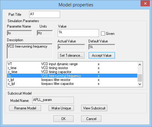 Setting the free-running frequency in the property dialog of the APLL block. |
The Transient Initial Condition Marker labeled IC1 with a prescribed voltage of 1V is placed at the output of the square wave VCO output to the give the oscillator circuit the initial kick.
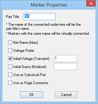 The property dialog of the Transient IC Marker. |
Define a sinusoidal waveform for your voltage source according to the table below:
|
|
V1: Sinusoid
| Offset Voltage
|
0
|
| Peak Amplitude
|
1
|
| Frequency
|
1kHz
|
| Delay Time
|
0
|
| Damping Factor
|
0
|
Run a Transient Test of this circuit with the parameters specified below:
|
|
| Start Time
|
0
|
| Stop Time
|
10m
|
| Linearize Step
|
1u
|
| Step Ceiling
|
1u
|
| Preset Graph Plots
|
v(1), v(4), v(5)
|
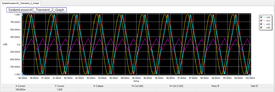
The voltage graphs are shown in the figure below. The RF.Spice's APLL device provides a square wave output as well as a triangular wave output, both of which are phase-locked with the input signal. This can be clearly seen from the figure by comparing the phases of the red input sinusoid and the light blue output triangular wave.
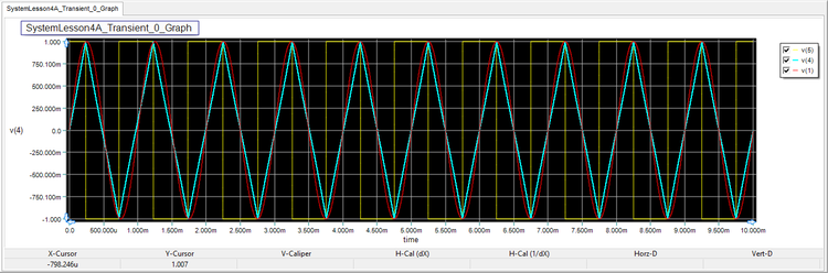 The graph of the input sinusoidal waveform and the output square wave and triangular waveforms of the APLL block. |
Examining the Effect of the Transient Initial Conditions
If the transient initial condition at the output of the VCO is zero, the initial phase difference will be zero. As result, the output of the phase detector will be zero and the feedback loop will not work. That's why you set up the marker IC1 to impose a nonzero initial voltage at Node 5. At this part of the tutorial lesson, use the same circuit as above and run an transient test with the following parameters:
|
|
| Start Time
|
0
|
| Stop Time
|
100m
|
| Linearize Step
|
1u
|
| Step Ceiling
|
1u
|
| Preset Graph Plots
|
v(2)
|
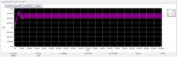
The figure below shows the voltage at the output of the loop filter. It can be seen that this phase error signal fluctuates between 194mV and -196mV with a zero average. The output signal is thus locked in phase and frequency with the input signal.
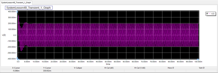 The graph of the phase error voltage signal over a long period time with IC1 = +1V. |
Next, change the value of the initial voltage of the IC1 marker to -0.1V and run a new transient test with the same parameters as before. As the figure below shows, the PPL still locks but it takes a little longer than the previous case.
 The graph of the phase error voltage signal over a long period time with IC1 = -0.1V. |
Investigating the Effect of a Frequency Step
Using the same circuit of the previous part and setting the value of IC1 voltage back to +1V, now change the frequency of the source signal to 1.05kHz. Note that the free-running frequency of the PLL is still the default 1kHz.
Run an transient test with the following parameters:
|
|
| Start Time
|
0
|
| Stop Time
|
100m
|
| Linearize Step
|
1u
|
| Step Ceiling
|
1u
|
| Preset Graph Plots
|
v(1), v(2), v(4)
|
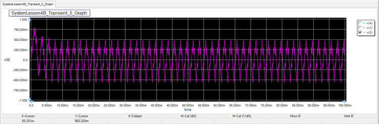
Initially, deselect the input and output signal plots in the graph's legend box and display the error voltage only as shown in the figure below. As you can see, v(2) fluctuates between -30mV and 330mV with an average of 150mV. This is the steady state phase error signal for the PLL to lock the output frequency.
 The graph of the phase error voltage signal for a signal frequency of 1.05kHz. |
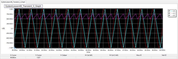
Next, enable all the three plots but change and scale the time (bottom) axis between 90ms and 100ms. As you can see from the figure below, the both the frequency and phase of the output signal has locked to the input signal.
 The graph of the input, output and phase error voltage signals with fs = 1.05kHz in the interval t = [90ms, 100ms]. |
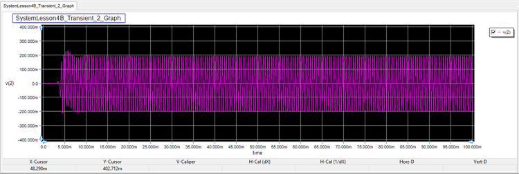
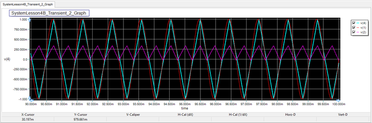
Repeat the same procedure this time with a source signal frequency of fs = 1.2kHz and plot the same graphs. This time v(2) fluctuates between 486mV and 760mV with a steady state average error of 623mV. The figure shows a reasonably good phase and frequency lock.
 The graph of the phase error voltage signal for a signal frequency of 1.2kHz. |
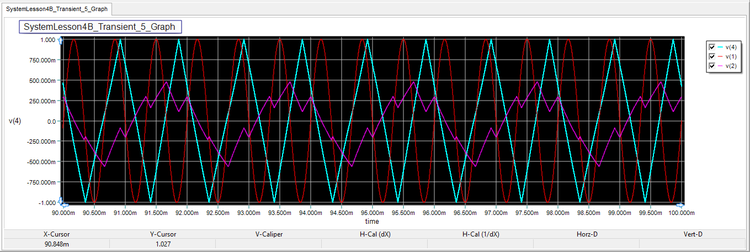
 The graph of the input, output and phase error voltage signals with fs = 1.2kHz in the interval t = [90ms, 100ms]. |
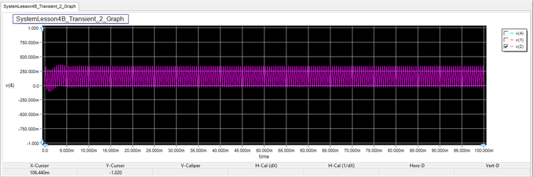
Finally, set the source signal frequency to fs = 1.5kHz and repeat the same simulation. This time, however, the PLL fails to lock either the frequency or phase of the output signal as you can clearly see fro the figures below.
 The graph of the phase error voltage signal for a signal frequency of 1.5kHz. |
 The graph of the input, output and phase error voltage signals with fs = 1.5kHz in the interval t = [90ms, 100ms]. |
Investigating the Effect of a Phase Step
The following is a list of parts needed for this part of the tutorial lesson:
|
|
| Part Name
|
Part Type
|
Part Value
|
| V1
|
Voltage Source
|
Waveform TBD
|
| A1
|
Analog Phase-Locked Loop (APLL)
|
Defaults
|
| X1
|
Ideal Phase Shifter Block
|
Defaults
|
| R1
|
Resistor
|
50
|
| IC1
|
Transient Initial Condition Marker
|
1V
|
Place and connect the parts as shown in the Figure below:
 The APLL circuit with an ideal phase shifter block at its input. |
You can access the phase shifter device from Menu > Parts > Analog Signal Processing Blocks > Signal Transformation Blocks > Ideal Phase Shifter Block. The phase shifter block is frequency-dependent. Enter a center frequency of 1kHz and set its Phase parameter to 45 degrees.
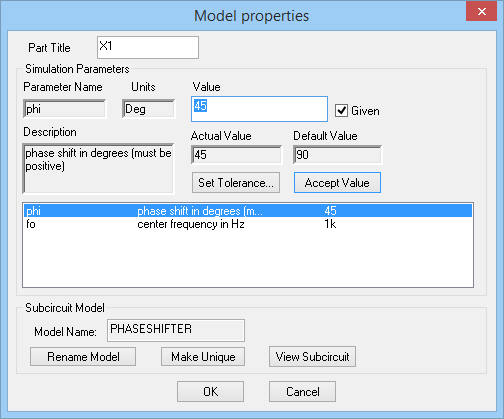 The property dialog of the Ideal Phase Shifter Block. |
Set the value of the IC1 voltage to +1V. Similar to the beginning of this project, define a sinusoidal waveform for your voltage source according to the table below:
|
|
V1: Sinusoid
| Offset Voltage
|
0
|
| Peak Amplitude
|
1
|
| Frequency
|
1kHz
|
| Delay Time
|
0
|
| Damping Factor
|
0
|
Run a Transient Test of this circuit with the parameters specified below:
|
|
| Start Time
|
0
|
| Stop Time
|
100m
|
| Linearize Step
|
1u
|
| Step Ceiling
|
1u
|
| Preset Graph Plots
|
v(1), v(2), v(4), v(6)
|
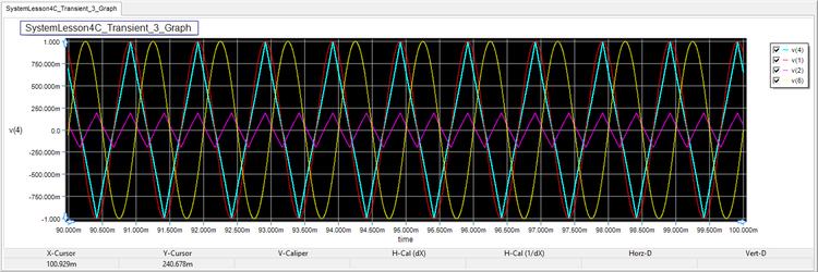
As you did in the previous section, repeat the same procedure of plotting the error signal first over the entire simulation period and then all the designated output signals over the time interval t = [90ms, 100ms]. You can see from the figure below that the PLL locks the output signal successfully.
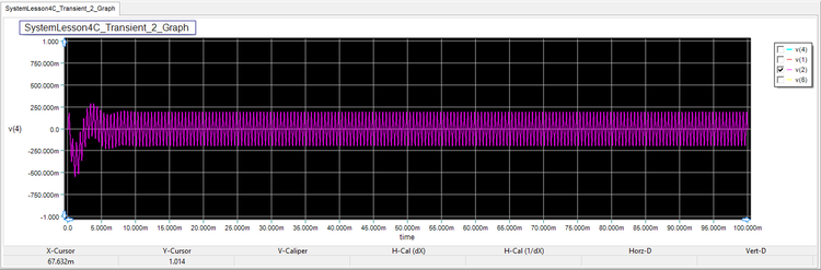 The graph of the phase error voltage signal for an input phase shift of 45°. |
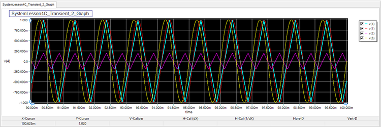 The graph of the source signal, phase-shifted input signal, output signal and phase error voltage with φ = 45° in the interval t = [90ms, 100ms]. |
Repeat the same simulation this time with a phase shift of 240°. For comparison, the original source signal and its phase-shifted version have both been plotted.
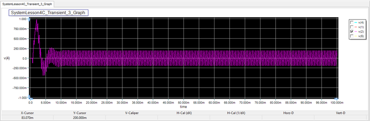 The graph of the phase error voltage signal for an input phase shift of 240°. |
 The graph of the source signal, phase-shifted input signal, output signal and phase error voltage with φ = 240° in the interval t = [90ms, 100ms]. |
 Back to RF.Spice A/D Tutorial Gateway


