EM.Tempo Tutorial Lesson 9: Modeling Coplanar Waveguide Structures And Lumped Devices
Contents
What You Will Learn
In this tutorial you will learn how to construct coplanar waveguide (CPW) transmission line structures with different termination types. You will learn about lumped devices like linear resistors and nonlinear diodes. You will examine temporal waveforms of different types for exciting your CPW structure and will investigate the transient response of your circuit. You will also learn how to parameterize geometric objects using independent and dependent variables.
![]() Back to EM.Tempo Tutorial Gateway
Back to EM.Tempo Tutorial Gateway
![]() Download projects related to this tutorial lesson
Download projects related to this tutorial lesson
Getting Started
Open the EM.Cube application and switch to EM.Tempo. Start a new project with the following attributes:
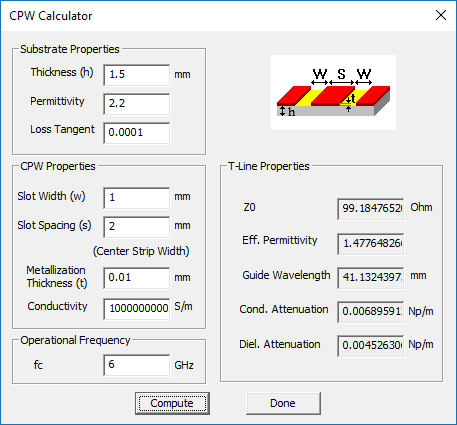
A coplanar waveguide with a slot width of w = 1mm and center metal strip width of s = 2mm on a dielectric substrate of thickness h = 1.5mm and εr = 2.2 has a characteristic impedance of Z0 = 99.18Ω and effective permittivity of εeff = 1.48. At an operating frequency of fo = 6GHz, the free-space and guide wavelengths are λ0 = 50mm and λg = λ0/√εeff = 41.13mm, respectively. You can verify these results using the CPW Transmission Line Calculator tool in the Device Manager of RF.Spice A/D, if you have installed it on your computer. You can access the Device Manager directly from the Tools Menu of EM.Tempo.
Building the CPW Geometry
Click on the CPW Wizard ![]() button of the Wizard Toolbar or select the menu item Tools → Transmission Line Wizards → Coplanar Waveguide.
button of the Wizard Toolbar or select the menu item Tools → Transmission Line Wizards → Coplanar Waveguide.
A one-port CPW structure is created in the project workspace. The transmission line segment is fed from the right edge of the substrate using a "Coplanar Waveguide Port Source" called "CPW_1". The two lateral ground planes "Ground_1" and "Ground_2" extend to the entire length of the substrate. The center metal strip is terminated in an open end at x = -25mm. The open-ended center strip itself consists of two rectangle strip objects called "ANCHOR" and "Feed".
First, open the variables dialog and change the definitions of a number of variables according to the table below:
| Variable Name | Original Definition | New Definition |
|---|---|---|
| h | 0.0015*to_meters | 1.5 |
| sub_len | 0.1*to_meters | 100 |
| sub_wid | 0.05*to_meters | 50 |
| center_len | 0.05*to_meters | 50 |
| feed_wid | 0.002*to_meters | 2 |
| center_wid | 0.002*to_meters | 2 |
| slot_wid | 0.002*to_meters | 1 |
Note that most of the changes above were done to express the dimension variables directly in the project units just for convenience. The slot width of the CPW line was the only variable that effectively changed the geometry of your CPW structure.
Now add three new variables, one independent and two dependent, according to the table below:
| Variable Name | Original Definition | New Definition |
|---|---|---|
| gap | N/A | 8 |
| rect_len | N/A | sub_len-center_len-feed_len-gap |
| rect_x | N/A | -sub_len/2+rect_len/2 |
The variables dialog should now look like this:
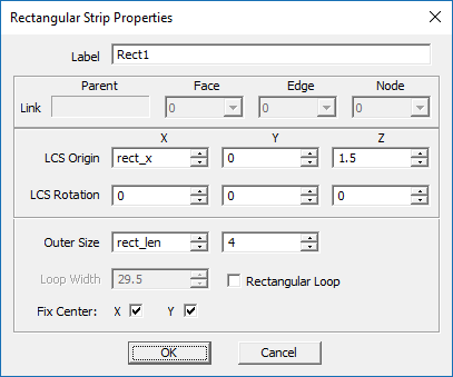
Next, make sure the PEC group "CONDUCTOR" is the active material group in the navigation tree. Then, add a PEC rectangle strip according to the table below:
| Part | Object Type | Material Type | Dimensions | Coordinates | Rotation Angles |
|---|---|---|---|---|---|
| Rect1 | Rectangle Strip | PEC | rect_len × 4mm | (rect_x, 0, 1.5mm) | (0°, 0°, 0°) |
Also, open the domain settings dialog and change the domain offset parameters according to the figure below:
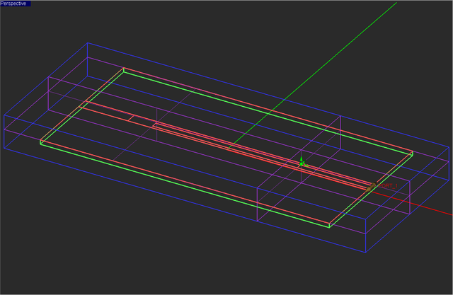
In this case, all the domain box faces are still PML walls. But the ±Z wall have been brought closer to the substrate as the structure does not radiate. The lateral ±Y now touch the substrate and model a laterally infinite substrate and ground along the ±Y directions. The geometry of your physical structure should now look like this:
A CPW source consists of a pair of special distributed sources that are associated with a PEC rectangle strip object. They are placed at one edge of the strip and extend out in opposite directions. The Spacing parameter of the CPW source is set equal to the slot width of the CPW transmission line. The name refers to the spacing between the strip and the two lateral ground plane objects. A CPW source is automatically set to launch the odd mode of a CPW transmission line. Open the property dialog of "CPW_1" from the navigation tree and examine its parameters. Change the internal source Resistance to 100Ω.
The wizard created the CPW source and automatically added a port definition to the navigation tree. Open the Port Definition dialog, select "Port_1", and using the dialog's Edit button, set the value of Reference Impedance to 100Ω.
Defining the Observables and Simulating the CPW Structure
For this project, you will define two temporal field probes and three near-field sensor observables according to the specifications below:
| Field Probe | Coordinates |
|---|---|
| Probe_1 | (25, 1.5mm, 1.5mm) |
| Field Sensor | Direction | Coordinates | Plot Type | Max. Size | Cone Length Ratio | Cone Radius Ratio |
|---|---|---|---|---|---|---|
| Sensor_1 | Z | (-25mm, 1.5mm, 1.5mm) | Vector | 0.5 | 0.5 | 0.25 |
| Sensor_2 | X | (25mm, 1.5mm, 1.5mm) | Vector | 0.5 | 0.5 | 0.25 |
| Sensor_3 | Y | (-25mm, 1.5mm, 1.5mm) | Intensity | - | - | - |
Note that the coordinates of the field probe and field sensors have been chosen to measure the field at the center of the positive slot line. Before you run an FDTD simulation of your CPW structure, do the following:
- Open the Mesh Settings dialog, click the button labeled High Precision Mesh Settings, and change the mesh density to 40 Cells/λeff.
- Open the Engine Settings dialog. In the section titled Termination Criterion, select the second radio button labeled Specify End Time and change the value of No. Time Steps to 2500.
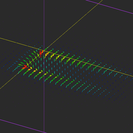
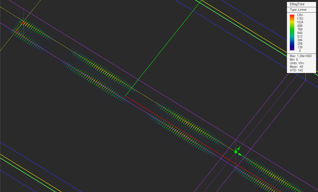
Run an FDTD simulation of your transmission line circuit and visualize its field distributions. The figure below shows the electric field distribution on a horizontal plane at z = 1.5mm, i.e. the surface of the CPW line. The E-field is almost zero everywhere except on the two slots. The fields are uniform longitudinally along the two slot lines, meaning that a decent impedance match has been accomplished and there is little wave reflection that would cause a standing wave pattern.
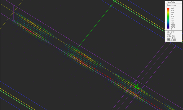
Note that the electric field at the open end is at its maximum while the magnetic field is at its minimum at that location. You can also clearly see the standing wave pattern of the fields along the transmission line. The distance between two consecutive field minima or maxima is equal to the half guide wavelength. This can easily be verified from the 2D graphs of field distributions. Open the data manager and plot the data file "Sensor_1_X_ETotal.DAT". Similar to the tutorial lesson 6, measure the distance between two field peaks in the graph. The figure below shows a spacing of 20.2mm. According RF.Spice A/D, half the guide wavelength for this CPW line is λg/2 = 20.56mm.
Examining the Temporal Waveforms on the CWP Line
The excitation source in a FDTD simulation pumps up energy into the computational domain and sets the initial conditions of the boundary value problem. By default, EM.Tempo uses modulated Gaussian waveform to excite all the sources. The default waveform starts after a short delay from t = 0, oscillates over a certain amount of time determined by the project bandwidth, reaches a maximum value in this interval and gradually decays to zero as t → ∞. In the CPW source dialog and all other source dialogs, you can click the Waveform... button to open the Excitation Waveform dialog. You can see a graph of the excitation waveform along with its mathematical expression and parameters in this dialog.
Open the data manager and plot the data file "Probe_1_Y_E_Time.DAT". This graph represents the temporal waveform at the locations of "Probe_1" at x = 25mm. You can see two pulses in the graph below. The first one represents the incident wave and the second one represents the reflected wave after hitting the open end discontinuity. You can measure the time interval between the peaks of the two pulses. It is about 0.42ns.
Next, you will verify this result using the fact that λg = λ0/√εeff. Therefore, εeff = (50/40.4)2 = 1.532, which is very close to the value calculated by RF.Spice A/D. The round-trip distance between the location of "Probe_1" and the open end discontinuity is drt = 100mm. The phase velocity of the propagation mode is vp = c0/√εeff. We can now calculate the round-trip time as:
[math] \Delta t_{rt} = \frac{d_{rt}}{v_p} = \frac{d_{rt}}{c_0} \sqrt{\epsilon_{eff}} = 0.413 ns [/math]
Terminating the CPW Line in a Resistive Load
In this section of the tutorial lesson, you will terminate the CPW line with a resistive load and will perform a parametric sweep of your circuit as a function of the load resistance. First, you will draw a horizontal line to connect the open end of the center strip to the object "Rect1", which is part of the ground plane. This will effectively short out the center strip. You have to make sure that the PEC material group called "CONDUCTOR" is the active group in the navigation tree. Under the PEC group, draw the following line object:
| Part | Object Type | Material Type | Dimensions | Coordinates | Rotation Angles |
|---|---|---|---|---|---|
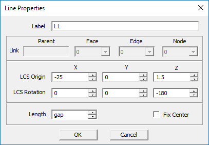
| L1 | Line | PEC | gap | (-25mm, 0, 1.5mm) | (0°, 0°, -180°) |
To draw a horizontal line, select the Line ![]() button of the Object Toolbar or select the menu item Object → Curve → Line.
button of the Object Toolbar or select the menu item Object → Curve → Line.
With the line tool selected, click on a block space and drag the mouse to start drawing a line. Observe the changing Length value in the dialog box and lock it in when the length reaches a desired value. Change the coordinates of the short vertical object to (-25mm, 0, 1.5mm) and the rotation angles to (0°, 0°, -180°).
Next, open the variables dialog and define a new variable called RR with a definition (numeric value) of 0. This will represent the resistance of the termination load. Also reduce the gap size to 1mm according to the table below:
| Variable Name | Original Definition | New Definition |
|---|---|---|
| gap | 8 | 1 |
| RR | N/A | 0 |
Now, right-click on the Lumped Devices item in the "Sources" section of the navigation tree and select Insert New Source... from the contextual menu. The lumped device dialog opens up. Change the name to "LC1". From the Line Object drop-down list, choose "L1". For the Offset parameter, enter the expression "gap/2". The Type drop-down list offers four options: Resistor, Capacitor, Inductor and Diode. Select Resistor and replace its default Resistance value of 100Ω with the variable "RR".
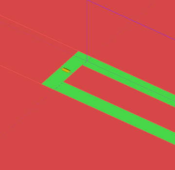
The lumped resistor at the end of the center strip will look like this:
Open EM.Tempo's simulation run dialog and select Parametric Sweep as the simulation mode. Open the parametric sweep settings dialog by clicking the Settings button. Select "RR" as your uniform sweep variable and set its start, stop and step values equal to 0Ω, 200Ω and 25Ω, respectively, as shown in the figure below:
Run a parametric sweep simulation of your resistively terminated CPW line and plot the S11 parameter (DP_S11.CPX). As you can see from the figure below, the return loss attains a minimum value of -13.0dB for RR = 100Ω.
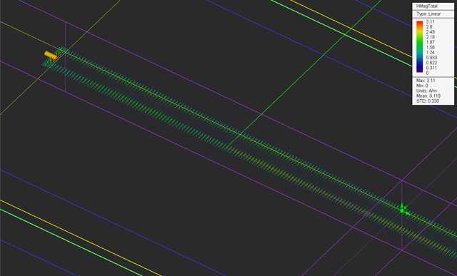
In the last part of this section, open the variables dialog and set the value of the variable "RR" equal to 100 Ohms. Then, run a "Wideband Analysis" of your CPW structure. Visualize the field distributions on the sensor planes and compare them to the case of no lumped resistor. From the figures below you can see that both the electric and magnetic field distributions on the CPW line are more uniform, an indicator of a reasonable impedance match.
Plot the data file "Sensor_1_X_ETotal.DAT". From this figure, too, you can see that the standing wave pattern along the CPW has subsided significantly compared to the previous case. The maximum and minimum field values are read to be |Emax| = 453V/m and |Emin| = 363V/m. The voltage standing wave ratio (VSWR) is defined as VSWR = |Vmax|/|Vmin| = |Emax|/|Emin| = 453/363 = 1.248.
Using a Nonlinear Diode
EM.Tempo's lumped device dialog gives you the option to define a nonlinear diode. A diode is a rectifying device. The time-domain relationship between the voltage and current of a diode is given by the nonlinear equation:
[math] i(t) = I_s \left( e^{\frac{kv(t)}{nqT}} - 1 \right) [/math]
where Is is the saturation current, k = 1.3806488 × 10⁻²³m2kg.s-2K-1 is the Boltzmann constant, q = 1.60217657 × 10⁻¹⁹ is the electron charge, T is the temperature in degrees Kelvin, and n is the ideality factor. The diode allows the flow of positive current in the direction from anode to cathode, but it blocks the flow of current in the opposite direction.
Open the property dialog of the lumped device "LC1", and from the Type drop-down list, select Diode. Enter the following parameters for the diode device:
| Line Object | L1 |
| Direction | -X |
| Saturation Current (Is) | 100fA |
| Temperature (K) | 300 |
| Ideality Factor | 1 |
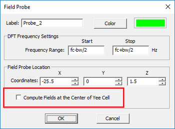
Define an additional temporal field probe at the location of the lumped diode device according to the specifications below:
| Field Probe | Coordinates |
|---|---|
| Probe_2 | (-25.5mm, 0, 1.5mm) |
Uncheck the "Compute Fields at the Center of Yee Cell" checkbox for both Field Probes.
For this part of the tutorial lesson, you are also going to change the excitation waveform for the first time. Open the property dialog of the CPW port source "CPW_1" and click its Waveform... button. In the Excitation waveform dialog, select the second radio button labeled Use Custom Frequency Domain Specifications. From the drop-down list labeled Waveform Type, select the Sinusoid option and enter a value of 5V for the Amplitude. Note that the default frequency is "fc". This means that your excitation waveform will be a single-tone harmonic waveform with f = fc = 6GHz with a period equal to T = 1/f = 0.167ns.
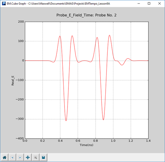
Run an FDTD simulation of your structure with a fixed number of 2,500 time steps. Plot the data files "Probe_1_Y_E_Time.DAT" and "Probe_2_X_E_Time.DAT", corresponding to the waveforms of Probe_1 and Probe_2, respectively. Note that the sinusoidal waveform starts after a delay of about 0.3ns, the time it takes to travel from the source location to the diode's location. Also, the period of the sinusoidal waveform is measured to be 0.167ns as expected.
You can clearly see the rectifying action of the nonlinear diode device from the above waveform. During the negative half-cycles, the input sinusoid is delivered to the load. During the positive half-cycles, the waveform is clipped from the top. This happens when the diode is reverse-biased. The positive constant field value during the reverse bias cycle is due to the voltage drop across the diode. Also, note that the waveform of the "Probe_1" close to the source is pure sinusoidal for the first 0.525ns and then starts to get distorted. This is when the reflected wave from the discontinuity reaches the location of this probe.
