EM.Tempo Tutorial Lesson 3: Modeling A Probe-Fed Microstrip Patch Antenna
Contents
- 1 What You Will Learn
- 2 Getting Started
- 3 Creating the Patch Antenna Geometry
- 4 Defining a Near-Field Sensor Observable
- 5 Running the FDTD Simulation & Visualizing the Results
- 6 Changing the Location of the Probe Feed
- 7 Changing the Geometry of the Square Patch
- 8 Performing a Parametric Sweep of the Rectangular Patch Antenna
What You Will Learn
In this tutorial you will use a wizard to build and analyze a probe-fed rectangular patch antenna on a finite-sized conductor-backed dielectric substrate. You will also learn how to use variables and run a parametric sweep simulation.
![]() Back to EM.Tempo Tutorial Gateway
Back to EM.Tempo Tutorial Gateway
![]() Download projects related to this tutorial lesson
Download projects related to this tutorial lesson
Getting Started
Open the EM.Cube application and switch to EM.Tempo. Start a new project with the following attributes:
Creating the Patch Antenna Geometry
As you did in the first tutorial lesson, you will use a wizard in this project to build the geometry of a rectangular patch antenna. Click on the Probe-Fed Patch Wizard ![]() button of the Wizard Toolbar or select the menu item Tools → Antenna Wizards → Probe-Fed Patch Antenna.
button of the Wizard Toolbar or select the menu item Tools → Antenna Wizards → Probe-Fed Patch Antenna.
The geometry of a rectangular patch antenna on a conductor-backed dielectric substrate appears in the project workspace along with a lumped source, a far field radiation pattern observable and a port definition. The table below shows a list of objects that constitute the patch antenna structure along with their material types and dimensions:
| Part | Object Type | Material Type | Dimensions |
|---|---|---|---|
| Substrate | Box | Dielectric | sub_size × sub_size × h |
| Patch_ANCHOR | Rectangle Strip | PEC | len × len |
| Ground | Rectangle Strip | PEC | sub_size × sub_size × h |
| Feed | Line | PEC | h |
The dimensions of the constituent objects have been parameterized. Open the variables dialog to see a list of the variables and their definitions. The initial value of the variable "sub_size" is 92.3976. This indicates the dielectric substrate is 92.3976mm × 92.3976mm × 1.5mm. Click the Edit button of the dialog to open the Edit Variable dialog. Replace this value by 150 in the box labeled Definition. Close this dialog to return to the variable dialog and check out the new value you just changed.
You can also see from the variables dialog that the dielectric substrate (represented by a box of dimensions 150mm × 150mm × 1.5mm) has a relative permittivity εr = 2.2 and a thickness h = 1.5mm. A short vertical line called "Feed" is placed underneath the patch and is completely embedded in the substrate. This line object serves as the probe feed of the patch antenna and is associated with a lumped source called "LS_1". There is also a far-field radiation pattern observable with the default theta and phi angle increments of 5° as well as a port definition with a reference port impedance of 50Ω. Also, note that the metallic patch is a square with its side dimensions set equal to len = 0.48λd, where λd is the effective dielectric wavelength.
Defining a Near-Field Sensor Observable
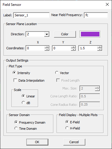
In order to observe the electric and magnetic field distributions on the patch, let's define a horizontal (Z-directed) field sensor plane parallel to the XY plane and located a Z = 1.5mm.
| |
The tangential magnetic field distribution on the patch is also representative of the electric surface current distribution on it. |
Running the FDTD Simulation & Visualizing the Results
At this time, your project is ready for FDTD simulation. Note that your antenna involves a very thin substrate layer. This requires a high resolution mesh to correctly represent the substrate thickness. The wizard automatically sets the mesh density to 40 cells/λeff. The fraction of the absolute minimum grid spacing to maximum grid spacing in the free space has been set to 0.05. Note that the Mesh settings dialog also provides a button labeled High Precision Mesh Settings that adjusts most of these parameters. The wizard's mesh settings for this particular geometry are even more demanding than the "high precision mesh settings.
Similar to the first tutorial lesson, the wizard sets up very demanding convergence criteria for this project, that is, a Power Threshold equal to -50dB and a Max No. Time Steps equal to 20,000. Run a Wideband Analysis of your patch antenna and visualize its near-field and far-field characteristics. The figure below shows the return loss of the patch antenna:
The figures below show the theta and phi components of the 3D radiation pattern as well as the total radiation pattern plot. Note that the directivity of the antenna is computed to be D0 = 6.242.
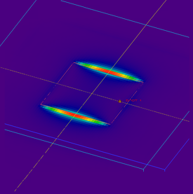
The figures below show the total electric and magnetic field distributions on the patch plane:
Changing the Location of the Probe Feed
The probe feed of your patch antenna is initially placed on the X-axis close to its right edge and its location is parameterized using a variable called "feed_ratio" with a default value of 0.4. This variable represents that offset of the probe feed from the center of the patch. In other words, feed_ratio = 0 means a center probe, while feed_ratio = 0.5 means the probe exactly on the edge of the patch. You can understand this better by noting the X-coordinate of the feed line, which is defined as feed_x = feed_ratio * len. To move the probe feed inward, open the variables dialog and select "feed_ratio". Click the Edit button of the dialog to open the Edit Variable dialog. The initial value of the variable is 0.4. Replace this value by 0.2 in the box labeled Definition. Close this dialog to return to the variable dialog and check out the new value you just changed.
Run a new FDTD analysis of your patch and plot its S11 parameter. Note that the new probe location provide a better return loss and a deeper resonance notch.
The radiation pattern of the patch and the the electric and magnetic field levels don't change much with the location of its probe feed. as seen in the figure below:
Changing the Geometry of the Square Patch
In this part of the tutorial lesson, you will turn the square patch into a rectangular patch with a larger width than its length. Both the X and Y dimensions of the patch were initially set equal to the variable "len". Now you define a new variable called "wid" with an initial value of 70mm. Open the variables dialog and click the Add button of the dialog to open the Add Variable dialog. Enter "wid" for the name and "70" for Definition. Return to the variables dialog and close it.
Next, open the property dialog of the object "Patch_ANCHOR". Replace the value of the box labeled Y "Outer Size" with "wid" and click the OK button of the property dialog to return to the project workspace. Note that width of the patch has slightly increased and it is no longer a square.
Performing a Parametric Sweep of the Rectangular Patch Antenna
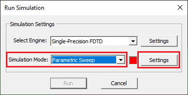
So far you have only run single-shot simulations of "Analysis" type. In a sweep simulation, one or more parameters are varied, and the simulation engine is run for each parameter set. Open the Simulation Run dialog and choose the Parametric Sweep option from the Simulation Mode drop-down list. Click on the Settings button next to this drop-down list to open the Sweep Settings dialog.
The sweep variables list is initially empty. On the left side of this dialog, you see a list of all the available independent variables. Select "wid" from the left table and used the --> button to move it to the right table. Another dialog titled "Sweep Variable" opens up. You have to set the start, stop and step values of your sweep variable. By default, the sweep variable is of uniform type. Enter 70, 100, and 10 for start, stop and step values, respectively. This will create a value list of {70, 80, 90, 100}. Close the sweep variable dialog and then close the sweep settings dialog to return to the simulation run dialog.
Run the sweep simulation. It may take a while as a total of four individual FDTD simulations must be completed. At each simulation, EM.Tempo generates a new mesh of the modified structure and passes it to the engine. At the end of the parametric sweep, open the data manager and plot the data file "DP_S11.CPX". You should see a graph like the following:
Note that the return loss is now plotted vs. the variable "wid" as opposed to frequency in the previous case. You can see that increasing the patch width only degrades the return loss and doesn't lead to a better impedance match. Since you also have a field sensor observable and a far field radiation pattern observable in your project, a plot is added to the navigation tree for each sweep sample. Therefore, you get a total of four field sensor plots and four radiation pattern plots. The figure below shows the total electric field distribution on the patch plane for the last sample of the variable wid = 100mm.


