| Part
|
Object Type
|
Direction
|
Dimensions
|
Coordinates
|
| Box_1
|
Box
|
N/A
|
1200mm × 600mm × 600mm
|
(0, 0, -300)
|
| IS_1
|
Ideal Source
|
+Z
|
Default
|
(-300mm, 0, 0)
|
| Probe_1
|
Field Probe
|
Z
|
N/A
|
(-300mm, 0, 0)
|
| Probe_2
|
Field Probe
|
Z
|
N/A
|
(300mm, 0, 0)
|
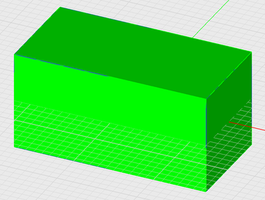 The geometry of the homogeneous dielectric medium with zero domain offsets at all six boundary walls. |
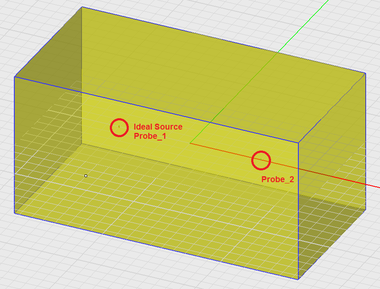 A see-through view of the homogeneous dielectric medium showing the location of the ideal source and probes. |
Set the FDTD mesh density to 12 cells per wavelength and keep all the other default mesh settings. Open the FDTD Engine Settings dialog from inside the Run dialog and set the Termination Criterion by specifying the "End Time" to 3,000 time steps. Run an FDTD analysis. At the end of the simulation, open the Data Manager and plot the time-domain electric field data for Probe_1 and Probe_2, as shown in the figures below:
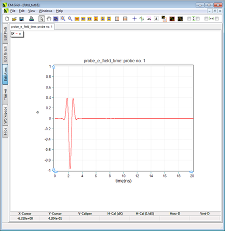 The input source waveform at Probe_1. |
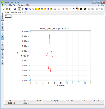
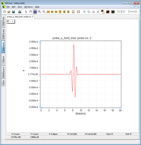 The output waveform at Probe_2 with ε r = 9. |
Probe_1 shows the ideal source waveform, which is a very compact modulated Gaussian waveform. Note that the center frequency of this waveform is 1GHz and its bandwidth is 2GHz. As you can see from the above figure, the source waveform has a delay of 2.173ns. This is the delay for an optimal modulated Gaussian waveform calculated from the following equation:
[math] T = \frac{(4.5)(0.966)}{BW} = \frac{(4.5)(0.966)}{2e+9} = 2.173 \times 10^{-9} s [/math]
On the other hand, the phase velocity in the dielectric medium is vp = c/√εr = c/3 = 1e+8 m/s. The distance between the source and observation probe is 600mm. The time it takes the source signal to reach the probe is therefore Δt = (0.6m)/vp = (0.6m)/(1e+8m/s) = 6e-9s = 6ns. With the initial 2.173ns delay, the peak signal must reach Probe_2 at t = 8.173ns, which is clearly seen from the above figure.
Next, change the relative permittivity of the Dielectric_1 group to εr = 4 and run the same simulation once again. The figure below shows the new waveform at Probe_2. in this case, the phase velocity in the dielectric medium is vp = c/√εr = c/2 = 1.5e+8 m/s. The time it takes the source signal to reach the probe is therefore Δt = (0.6m)/vp = (0.6m)/(1.5e+8m/s) = 4e-9s = 4ns. With the initial 2.173ns delay, the peak signal reaches Probe_2 at t = 6.173ns, which is 2ns earlier than the previous case.
 The output waveform at Probe_2 with ε r = 4. |
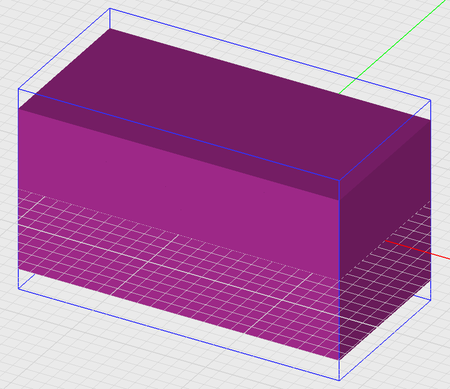
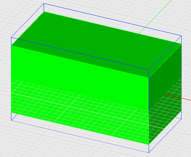 The geometry of the laterally infinite dielectric slab with zero domain offsets at the four side boundary walls. Modeling a Dielectric Slab
In this part of the tutorial lesson, you will consider a dielectric slab of finite thickness but with infinite lateral extents. To accomplish this, all you need to do is to keep the zero domain offsets in the ±X and ±Y directions and move the PML boundary walls away from the dielectric box at the top and bottom of the computational domain by a quarter free-space wavelength. For this purpose, set the values of the ±Z offsets equal to 0.25. The opposite figure shows the geometry setup for the dielectric slab.
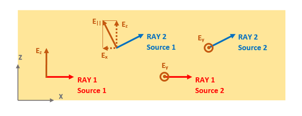
In the boundless homogeneous medium of the previous part, you could assume a direct ray carrying the source signal from the source location to the probe location 600mm away. In the case of the dielectric slab, besides the direct ray, there will be a number of reflected rays as shown in the figure below. These rays hit the top or bottom air-dielectric interfaces and are reflected towards the probe. It is evident that the optical paths the reflected rays traverse to reach the observation point at the location of Probe_2 are longer than the optical path of the direct ray, which is 600mm.
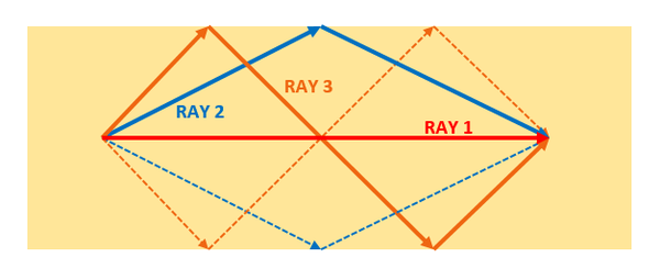 A diagram showing the direct and reflected rays leaving the ideal source and arriving at Probe_2. |
The following table shows the optical path lengths and travel times for the three rays shown in the above figure. Note that a phase velocity of vp = c/3 = 1e+8 m/s has been used for the calculations.
| Ray
|
Type
|
Optical Path Length
|
Travel Time
|
Arrival Time at Probe_2
|
| Ray 1
|
Direct
|
600mm
|
6ns
|
8.173ns
|
| Ray 2
|
Singly Reflected
|
848.5mm
|
8.485ns
|
10.658ns
|
| Ray 3
|
Doubly Reflected
|
1341.6mm
|
13.42ns
|
15.593ns
|
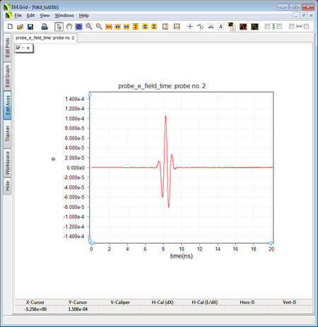
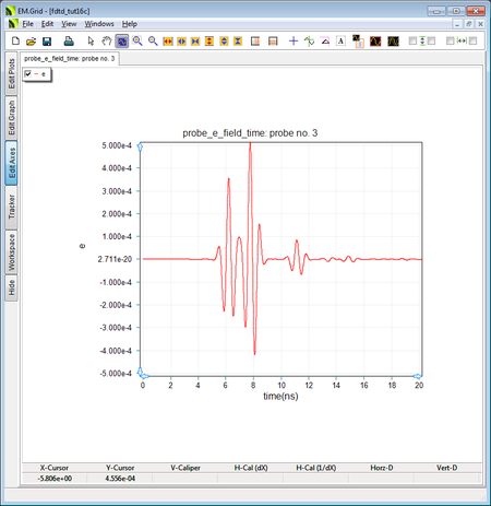
Set the permittivity of the Dielectric_1 group back to εr = 9, and run an FDTD analysis of your dielectric slab with the same ideal source and field probes of the previous part. In the figure below, you can clearly see three distinct modulated Gaussian pluses corresponding to Rays 1, 2, and 3, with their peaks centered at times 8.173ns, 10.658ns and 15.593ns, respectively.
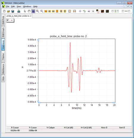 The output waveform at the Z-directed Probe_2 with ε r = 9 and a Z-directed ideal source. |
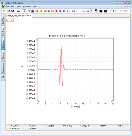
Next, change the permittivity of the Dielectric_1 group to εr = 4, and run another FDTD analysis. In this case, the phase velocity is vp = c/2 = 1.5e+8 m/s. The following table shows the optical path lengths and travel times for the three rays:
| Ray
|
Type
|
Optical Path Length
|
Travel Time
|
Arrival Time at Probe_2
|
| Ray 1
|
Direct
|
600mm
|
4ns
|
6.173ns
|
| Ray 2
|
Singly Reflected
|
848.5mm
|
5.567ns
|
7.83ns
|
| Ray 3
|
Doubly Reflected
|
1341.6mm
|
8.944ns
|
11.18ns
|
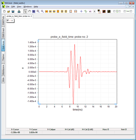
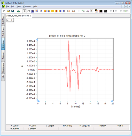
You are going to run two simulations at this point. In the first simulation, keep the Z-directed ideal source and Z-directed field probes as in the earlier parts. In the second simulation, change the direction of the ideal source and field probes to +Y. Run an FDTD analysis for each case and compare the output waveforms at Probe_2. Both of the figures below show three distinct modulated Gaussian pluses corresponding to Rays 1, 2, and 3, with their peaks centered at times 6.173ns, 7.83ns and 11.18ns, respectively. Note that in the case of Z-directed and Y-directed sources, the reflected rays have parallel and perpendicular polarizations with respect to the plane of incidence, respectively. The polarization type explains the inversion of the fields of the reflected ray in the first case and no field inversion in the second case. Also,, note that the doubly reflected Ray 3 undergoes two field inversions in the first case.
 The output waveform at the Z-directed Probe_2 with ε r = 4 and a Z-directed ideal source. |
 The output waveform at the Y-directed Probe_2 with ε r = 4 and a y-directed ideal source. |
Modeling an Anisotropic Material Medium
In this part of the tutorial lesson, you will examine an anisotropic medium. Define an anisotropic material group called ANI_1 in the Navigation Tree. In the Anisotropic Material dialog, you see a checkbox labeled "Uniaxial", which is checked by default. This means that your four constitutive tensors are diagonal by default. This is slightly different than the uniaxial and biaxial material definitions in Optics, whereby both material types have a diagonal permittivity tensor. For this project, define εrxx = 2, εryy = 4, and εrzz = 9.
Under the ANI_1 group, draw a box of the same dimension as in the case of the homogeneous material medium. Set up two Z-directed and Y-directed ideal sources both collocated at (-300mm, 0, 0) and set up three field probes as shown in the table below:
| Part
|
Object Type
|
Direction
|
Dimensions
|
Coordinates
|
| Box_1
|
Box
|
N/A
|
1200mm × 600mm × 600mm
|
(0, 0, -300)
|
| IS_1
|
Ideal Source
|
+Z
|
Default
|
(-300mm, 0, 0)
|
| IS_2
|
Ideal Source
|
+Y
|
Default
|
(-300mm, 0, 0)
|
| Probe_2
|
Field Probe
|
Z
|
N/A
|
(300mm, 0, 0)
|
| Probe_3
|
Field Probe
|
Y
|
N/A
|
(300mm, 0, 0)
|
Set all the six domain offset values to zero in all directions. Your structure now models an anisotropic medium of infinite extents.
 |
In the current version of EM.Cube's FDTD Module, anisotropic materials with nonzero off-diagonal constitutive tensor elements must be finite-sized and cannot touch the PML boundary wall. You can model infinite uniaxial anisotropic media with nonzero diagonal elements only.
|
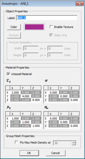 The Anisotropic Material dialog. |
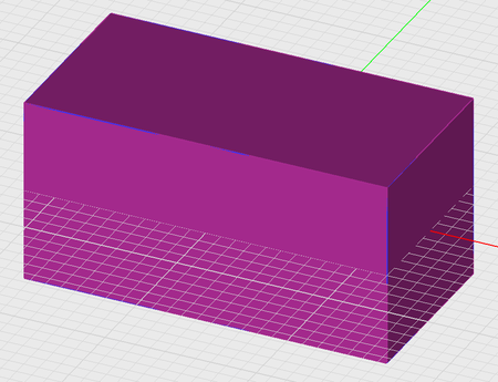 The geometry of the anisotropic medium with zero domain offsets at all six boundary walls. |
Run an FDTD analysis of your anisotropic medium. In this case, there will be two direct rays from the two ideal sources to the observation point. One ray is Z-polarized and sees a medium relative permittivity of 9, while the other ray is Y-polarized and sees a medium relative permittivity of 4. Note that the phase velocities of the two rays are different and equal to vpz = c/3 = 1e+8m/s and vpy = c/2 = 1.5e+8m/s, respectively. The figures below show the Z and Y components of the electric field at the observation point where Probe_2 and Probe_3 are located. Also, note that similarity of these waveforms to those of the homogeneous dielectric medium with permittivity values of 9 and 4 in the first part of this tutorial lesson.
 The output waveform at the Z-directed Probe_2 inside the unbounded anisotropic medium. |
 The output waveform at the Y-directed Probe_3 inside the unbounded anisotropic medium. |
 The geometry of the laterally infinite anisotropic slab with zero domain offsets at the four side boundary walls. Modeling an Anisotropic Material Slab
Take the geometry of the anisotropic structure from the last part, keep the zero values for the ±X and ±Y domain offsets, and change the value of the ±Z domain offsets to 0.25 as in the case of the dielectric slab. Also keep the two collocated ideal sources IS_1 and IS_2 and the two collocated field probes Probe_2 and Porbe_3 from the last part. Run an FDTD analysis of your anisotropic slab and plot the field probe data for the Z and Y components of the electric field.
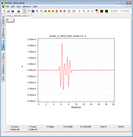
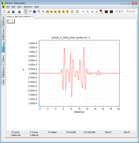
 The output waveform at the Z-directed Probe_2 inside the anisotropic slab with ε rxx = 2, ε ryy = 4, and ε rzz = 9. |
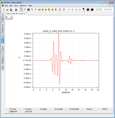
 The output waveform at the Y-directed Probe_3 inside the anisotropic slab with ε rxx = 2, ε ryy = 4, and ε rzz = 9. |
From the above figures, you can see that the first modulated Gaussian pulse of the Ez component (Probe_2) arrives at 8.173ns, while the first modulated Gaussian pulse of the Ey component (Probe_3) arrives at 6.173ns. These are consistent with the results you got earlier for the isotropic dielectric slab. The first Ez pulse resembles that of an isotropic dielectric slab with εr = 9 excited by a Z-directed source. The first Ey pulse resembles that of an isotropic dielectric slab with εr = 4 excited by a Y-directed source. However, the pulses corresponding to the reflected rays are completely different than their isotropic counterparts. This is due to the anisotropic nature of your new slab. As shown in the figure below, the reflected rays are decomposed to parallel and perpendicular polarizations. The parallel-polarized reflected rays have both Z- and X-directed field components. Since εrxx = 2, the X-polarized reflected rays will experience a faster phase velocity of vpx = c/√2 = 2.12e+8m/s and arrive at the observation point earlier than the Z-polarized reflected rays.
 A diagram showing the field components of the direct and reflected rays with parallel and perpendicular poarlizations. |
The anisotropic material just considered is typical of a biaxial optical crystal, where all the three diagonal permittivity elements have different values. Next, open the property dialog of the ANI_1 material group and change the diagonal permittivity elements to εrx = 9, εry = 4, and εrz = 9. This material is now typical of a uniaxial optical crystal, where two of the diagonal permittivity elements have identical values different than the third element.
Run an FDTD analysis of your new anisotropic slab and plot the field probe data for the Z and Y components of the electric field.
 The output waveform at the Z-directed Probe_2 inside the anisotropic slab with ε rxx = 9, ε ryy = 4, and ε rzz = 9. |
 The output waveform at the Y-directed Probe_3 inside the anisotropic slab with ε rxx = 9, ε ryy = 4, and ε rzz = 9. |
In this case, both the Z- and X-polarized reflected rays with parallel polarization see the same relative permittivity of 9 and experience the same phase velocity of vp|| = c/3 = 1e+8m/s. On the other hand, the Y-polarized reflected rays with perpendicular polarization see a relative permittivity of 4 and experience a phase velocity of vpy = c/2 = 1.5e+8m/s. As a result, the second and third Ez pulses resemble those of an isotropic dielectric slab with εr = 9 excited by a Z-directed source. The second and third Ey pulses resemble those of an isotropic dielectric slab with εr = 4 excited by a Y-directed source.
 Back to EM.Tempo Tutorial Gateway Back to EM.Tempo Tutorial Gateway
Back to EM.Cube Wiki Main Page
|
|
|
|


