EM.Picasso Tutorial Lesson 9: Designing a Microstrip Wilkinson Power Divider
Contents
- 1 What You Will Learn
- 2 Getting Started
- 3 Drawing the Power Divider Structure & Assigning Its Ports
- 4 Running a Frequency Sweep of the Power Divider
- 5 Adding a Lumped Resistor Between the Output Arms
- 6 Examining the Planar Mesh of the Power Divider with the Lumped Resistor
- 7 Simulating the Complete Wilkinson Power Divider
What You Will Learn
In this tutorial you will build and simulate a three-port planar circuit. You will also learn how to define a lumped element on a strip object to represent a lumped resistor.
![]() Back to EM.Picasso Tutorial Gateway
Back to EM.Picasso Tutorial Gateway
![]() Download projects related to this tutorial lesson
Download projects related to this tutorial lesson
Getting Started
Open the EM.Cube application and switch to EM.Picasso. Start a new project with the following parameters:
Drawing the Power Divider Structure & Assigning Its Ports
Create a PEC group called "PEC_1" on the navigation tree. The Wilkinson power divider will will consist of two different microstrip line types with characteristics impedance values of Z0 = 50Ω and √2Z0 = 70.7Ω. On the particular substrate of this project as specified in the above table, the widths of the two microstrip lines will be 2.4mm and 1.4mm, respectively. The ring strip will serve as the two 70.7Ω quarter-wave arms of the Wilkinson power divider. You can use Circle Strip Tool to draw rings and arcs using its "Outer Radius", "Inner Radius", "Start Angle" and "End Angle" parameters.
Draw a circle strip object with the following parameters.
| Label | Object Type | LCS Origin | Inner Radius | Outer Radius | Start Angle | End Angle |
|---|---|---|---|---|---|---|
| Circ_Strip_1 | Circle Strip | (0, 0, 0.787mm) | 8.25mm | 9.65mm | 20° | 340° |
To draw a rectangle, click the Circle Strip ![]() button of the Object Toolbar or select the menu item Object → Surface → Circle Strip.
button of the Object Toolbar or select the menu item Object → Surface → Circle Strip.
Next, draw six rectangle strip objects with dimensions and locations given in the table below:
| Label | Object Type | LCS Origin | X Dimension | Y Dimension |
|---|---|---|---|---|
| Rect_Strip_1 | Rectangle Strip (50Ω Input Line) | (-10.75mm, 0, 0.787mm) | 5mm | 2.4mm |
| Rect_Strip_2 | Rectangle Strip (50Ω Input Line) | (8.95mm, -5.3mm, 0.787mm) | 2.4mm | 5mm |
| Rect_Strip_3 | Rectangle Strip (50Ω Input Line) | (8.95mm, 5.3mm, 0.787mm) | 2.4mm | 5mm |
| Rect_Strip_4 | Rectangle Strip (50Ω Input Line) | (-17.25mm, 0, 0.787mm) | 8mm | 2.4mm |
| Rect_Strip_5 | Rectangle Strip (50Ω Input Line) | (8.95mm, -11.8mm, 0.787mm) | 2.4mm | 8mm |
| Rect_Strip_6 | Rectangle Strip (50Ω Input Line) | (8.95mm, 11.8mm, 0.787mm) | 2.4mm | 8mm |
Define three scattering wave port sources and assign them to the last three strip objects according to the table below:
| Source Label | Host Strip Object | Direction |
|---|---|---|
| WP_1 | Rect_Strip_4 | +X |
| WP_2 | Rect_Strip_5 | +Y |
| WP_3 | Rect_Strip_6 | -Y |
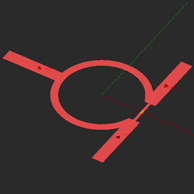
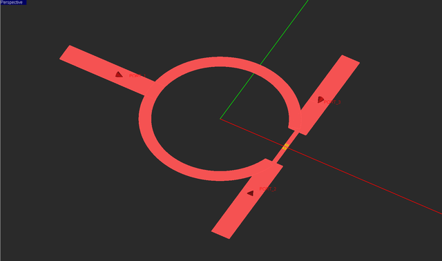
Your physical structure will look like this:
Open the planar mesh settings dialog and change the mesh density to 30 cells per effective wavelength. Generate the mesh of your physical structure as shown in the figures below.
Running a Frequency Sweep of the Power Divider
Run a frequency sweep of your Wilkinson power divider to examine its frequency response including return losses and insertion losses. Open the frequency sweep settings dialog from the run dialog and set the following uniform frequency sweep parameters:
| Start Frequency | 2GHz |
|---|---|
| End Frequency | 3GHz |
| Number of Frequency Samples | 11 |
So far in all the previous tutorial lessons, when you ran a frequency sweep (either uniform or adaptive), you kept the default option of meshing the structure at the highest frequency. For this project, select another option and mesh the structure at the center frequency of the project, i.e. at 2.4GHz. For non-resonant structure, these options don't make too much of a difference.
At the end of the sweep simulation, graph three data files: “S11_Sweep.CPX”, “S22_Sweep.CPX”, “S21_Sweep.CPX” and “S32_Sweep.CPX”. Make sure to scale the plots properly. From the figures below, you can see that the insertion loss values |S21| and |S31| are about -3dB over the entire frequency range. However, the output return losses |S22| and |S33| are about -6dB, which aren't good at all. You would also like to decrease the coupling |S32| between the two output ports to much lower than -7dB.
Adding a Lumped Resistor Between the Output Arms
In this part of the tutorial lesson, you will add a lumped resistor between the two output ports of your power divider to complete the Wilkinson design. But first you need to draw a narrow microstrip line segment between the two objects Rect2 and Rect3 to hold the lumped element.
| |
In EM.Picasso, a lumped element can only be defined in association with an existing rectangle strip object to serve as its host. |
Draw a new rectangle strip object with the following parameters:
| Label | Object Type | LCS Origin | X Dimension | Y Dimension |
|---|---|---|---|---|
| Rect_Strip_7 | Rectangle Strip | (8.95mm, 0, 0.787mm) | 0.5mm | 5.6mm |
Now you can define a lumped element to model your resistor. Go to the "Sources" section of the navigation tree, right-click on the Strip Gap Circuits item and select Insert New Source... from the contextual menu. in the source dialog, choose the name of the host line "Rect_Strip_7" from the drop-down list. Select Passive RLC for the lumped circuit type.
Click on the Impedance... button of this dialog to open the lumped element impedance dialog. By default the box labeled "Rs (Ohm)" is checked with a default resistance value of 50Ω. Change the value of resistance to 100Ω, i.e. 2Z0. Close the two nested dialogs and return to the project workspace. You will see a yellow lumped element appear at the center of the last strip object.
Examining the Planar Mesh of the Power Divider with the Lumped Resistor
The presence of the narrow microstrip line segment hosting the resistive lumped element acts like a discontinuity. As a result, it requires a high resolution mesh even though the segment's size is quite small. Open the planar mesh settings dialog and check the box labeled Refine Mesh at Gap Locations.
Now generate the mesh of the planar structure with the same mesh density of 30 cells per effective wavelength.
Simulating the Complete Wilkinson Power Divider
Run a frequency sweep of your Wilkinson power divider with the added resistor. Set the following uniform frequency sweep parameters and keep the option to mesh the structure at the center frequency of the project during the entire sweep.
| Start Frequency | 2GHz |
|---|---|
| End Frequency | 3GHz |
| Number of Frequency Samples | 11 |
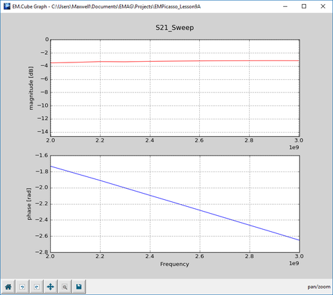
At the end of the sweep simulation, graph three data files: “S11_Sweep.CPX”, “S22_Sweep.CPX”, “S21_Sweep.CPX” and “S32_Sweep.CPX”. Make sure to scale the plots properly.
From the above figures, you can see that all three port are well matched. The insertion loss at the two output ports is -3.14dB, and the coupling between the output ports has dropped to lower than -18dB. The table below shows the values of all the S-parameters at the center frequency of the project fc = 2.4GHz.
| S-Parameter | Complex Value | Magnitude |
|---|---|---|
| S11 | 0.127755 +0.137375j | -14.535409dB |
| S12 | -0.399210 -0.570641j | -3.142585dB |
| S13 | -0.396975 -0.572491j | -3.139583dB |
| S21 | -0.400058 -0.570110j | -3.141940dB |
| S22 | 0.054326 +0.044426j | -23.075952dB |
| S23 | -0.065975 -0.102684j | -18.269098dB |
| S31 | -0.396755 -0.572401j | -3.142068dB |
| S32 | -0.065172 -0.103138j | -18.272559dB |
| S33 | 0.052328 +0.038422j | -23.752571 |


