EM.Picasso Tutorial Lesson 7: Designing A Slot-Coupled Patch Antenna
Contents
- 1 What You Will Learn
- 2 Getting Started
- 3 Creating the Slot-Coupled Patch Antenna Geometry
- 4 Examining the Multilayer Substrate's Layer Hierarchy
- 5 Running a PMOM Analysis of the Multilayer Antenna
- 6 Tuning the Patch's Resonant Length
- 7 Tuning the Length of the Open Microstrip Stub
- 8 Verifying Your Optimized Slot-Coupled Patch Antenna
- 9 Running a Frequency Sweep of the Optimized Slot-Coupled Patch Antenna
What You Will Learn
In this tutorial you will simulate multilayer planar structures that contain several metal and slot objects located on different trace planes. You will also learn how to set up a constrained parametric sweep that ties up different object parameters.
![]() Back to EM.Picasso Tutorial Gateway
Back to EM.Picasso Tutorial Gateway
![]() Download projects related to this tutorial lesson
Download projects related to this tutorial lesson
Getting Started
Open the EM.Cube application and switch to EM.Picasso. Start a new project with the following parameters:
Creating the Slot-Coupled Patch Antenna Geometry
Click on the Slot-Coupled Patch Wizard ![]() button of the Wizard Toolbar or select the menu item Tools → Antenna Wizards → Slot-Coupled Patch Antenna.
button of the Wizard Toolbar or select the menu item Tools → Antenna Wizards → Slot-Coupled Patch Antenna.
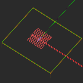
The wizard creates the geometry of the patch antenna in the project workspace.
Open the variables dialog and change the definition of the following variables:
| Variable Name | Original Definition | New Definition |
|---|---|---|
| er_patch | 2.2 | 3.38 |
| h_patch | 0.0015*to_meters | 2 |
| er_feed | 2.2 | 3.38 |
| h_feed | 0.0015*to_meters | 0.787 |
| feed_len | 1*patch_len | 30 |
| slot_len | 0.25*patch_len | 12 |
| slot_wid | 0.025*patch_len | 1.5 |
The variables list now looks like this:
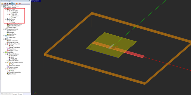
The wizard created three trace plane according to the table below:
| Trace Label | Trace Type | Function | Trace Location |
|---|---|---|---|
| PATCH_PEC | PEC Trace | Patch Plane | Between Top Substrate Layer and Top Half-Space |
| SLOT | Slot Trace | Coupling Slot Plane | Between Top Substrate Layer and Bottom Substrate Layer |
| FEED_PEC | PEC Trace | Microstrip Feed Plane | Between Bottom Substrate Layer and Bottom Half-Space |
Examining the Multilayer Substrate's Layer Hierarchy
Open EM.Picasso's stackup manager dialog and inspect the hierarchy of the substrate layers and interspersed trace planes.
You can assign different colors to different substrate layers. In the stackup manager, select and highlight the dielectric layer called "Patch Substrate" and click the Edit button of the dialog to open the substrate layer dialog. Click on the Color button to open Windows' standard color palette and choose green for the color of this layer.
Once you return to the project workspace, your physical structure will look like this:
The wizard created the following set of geometric objects, which together constitute your slot-coupled patch antenna structure:
| Label | Object Type | Trace Group | Length | Width |
|---|---|---|---|---|
| ANCHOR | Rectangle Strip | PATCH_PEC | patch_len | patch_len |
| slot | Rectangle Strip | SLOT | slot_wid | slot_len |
| Open_stub | Rectangle Strip | FEED_PEC | stub_len | feed_wid |
| Feed | Rectangle Strip | FEED_PEC | feed_len | feed_wid |
Running a PMOM Analysis of the Multilayer Antenna
The wizard already defined a scattering wave port called "WP_1" and associated it with the "Feed" object. It also initiated a default far-field radiation pattern observable as well as three current distribution observables, one for each trace group.
| |
In EM.Picasso, each individual trace plane requires its own current distribution observable. PEC traces have electric surface current distribution plots in A/m, while slot traces have magnetic surface current distribution plots in V/m. |
The wizard also set the mesh density of the antenna structure to 30 cells/λeff as shown in the figure below:
Run a quick single-frequency PMOM analysis of your multilayer planar structure. At the end of the simulation, the following port characteristic values are reported in the output message window:
S11: -0.684217 +0.056196j
S11(dB): -3.266925
Z11: 9.308750 +1.978907j
Y11: 0.102781 -0.021850j
Visualize all the three current distributions on the patch, slot and feed planes. Notice the standing wave pattern on the microstrip feed line.
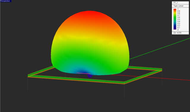
Visualize the 3D radiation pattern of your antenna. Note the portion of the radiation pattern in the lower half-space (90° ≤ θ ≤ 180°).
Tuning the Patch's Resonant Length
In this part of the tutorial lesson, you will vary the size of the top patch to find the resonant length. Open the variables dialog and change the definition of two variables: "patch_len" and "stub_len" to numeric values of "32" and "20", respectively. This change turns both of them into independent variables that can be designated as sweep variables.
Now run a parametric sweep of the variable "patch_len" according to the table below:
| Sweep Variable Name | patch_len |
|---|---|
| Sweep Variable Type | Uniform |
| Start Value | 31mm |
| Stop Value | 33mm |
| Step Value | 0.2mm |
Plot the data file "S11_Sweep.CPX". You can see that the return loss is minimized for a value pf patch_len between 31.6mm and 31.8mm. Open the variables dialog and set the value of "patch_len" equal to 31.7mm for the next part of the lesson.
Tuning the Length of the Open Microstrip Stub
The length of the open stub is usually set to extend λg/4 beyond the location of the coupling slot, where λg is the guide wavelength of the microstrip line. In this part of the tutorial lesson, you will perform a parametric sweep of the variable "sub_length". Note that you already fixed the value of "patch_len" at its optimal value of 31.7mm. Use the following parameters for the sweep variable "stub_len":
| Sweep Variable Name | stub_len |
|---|---|
| Sweep Variable Type | Uniform |
| Start Value | 20mm |
| Stop Value | 24mm |
| Step Value | 0.25mm |
Plot the data file "S11_Sweep.CPX". You will find that the return loss is minimized for a value pf "stub_len" around 23.5mm. Open the variables dialog and set the value of "stub_len" equal to 23.5mm for the next part of the lesson.
Verifying Your Optimized Slot-Coupled Patch Antenna
At this point, your slot-coupled patch antenna structure must have all the optimal values of the design variables.
Run a single-frequency analysis of your antenna to verify its return loss and the quality of the current distribution maps. At the end of the simulation, the following port characteristic values are reported in the output message window:
S11: 0.029379 -0.009350j
S11(dB): -30.220259
Z11: 53.017276 -0.992318j
Y11: 0.018855 +0.000353j
Visualize all the three current distributions on the patch, slot and feed planes. You can see from the current distribution on the microstrip feed line that the standing wave pattern you saw earlier is gone. A more uniform current distribution on the feed line is now observed, which is an indication of a good impedance match.
Running a Frequency Sweep of the Optimized Slot-Coupled Patch Antenna
To examine the resonant behavior and bandwidth of your slot-coupled patch antenna, run an adaptive frequency sweep with the following parameters:
| Start Frequency | 2GHz |
|---|---|
| End Frequency | 3GHz |
| Min. Number of Frequency Samples | 5 |
| Max. Number of Frequency Samples | 15 |
| Convergence Criterion | 0.02 |
After the completion of the frequency sweep simulation, plot the data file "S11_RationalFit.CPX". The return loss (|S11|) graph has a minimum of about -32dB at 2.4GHz with a 10-dB bandwidth of about 35MHz.


