EM.Illumina Tutorial Lesson 4: Simulating Radiation In The Presence Of Large Metallic Shipboard Platforms
Contents
What You Will Learn
In this tutorial you will learn how to import an external CAD model and set up a large-scale physical optics simulation in the EM.Illumina.
![]() Back to EM.Illumina Tutorial Gateway
Back to EM.Illumina Tutorial Gateway
![]() Download projects related to this tutorial lesson
Download projects related to this tutorial lesson
Getting Started
Open the EM.Cube application and switch to EM.Illumina. Start a new project with the following parameters:
For this tutorial lesson, you need to import a STEP CAD model file called "Ship.STP" from our File Repository. Make sure you have chosen meters as the unit project.
Importing the Ship Model
In EM.Cube, external objects are always imported to CubeCAD ![]() first. From CubeCAD you can transfer an imported object to any of the other computational modules. To import the ship model, go to File Menu and select Import.... The standard Windows Open dialog opens up with the file type set to ".STP". Browse your folders to find the downloaded CAD model file named "Ship.STP". Select it and click the Open button. A total 12 solid CAD objects appear in the project workspace of the CubeCAD Module as shown in the figure below:
first. From CubeCAD you can transfer an imported object to any of the other computational modules. To import the ship model, go to File Menu and select Import.... The standard Windows Open dialog opens up with the file type set to ".STP". Browse your folders to find the downloaded CAD model file named "Ship.STP". Select it and click the Open button. A total 12 solid CAD objects appear in the project workspace of the CubeCAD Module as shown in the figure below:
Now go to the EM.Illumina tab and create a PEC group called PEC_1 in EM.Illumina's navigation tree. To do so, right-click on the PEC Surfaces item under "Physical Structure" and select Insert New PEC... from the contextual menu. The property of the newly created PEC group opens up. The default name of the group is "PEC_1" and its default color is rosy red. Accept the default settings and close the dialog.
Next, you have to move all the imported solids to the PEC_1 group of EM.Illumina. To do so, select all the solid names on the navigation tree of the CubeCAD module. Start with Solid_1 and select it. Then, hold down the keyboard's Shift key and click Solid_12. While still holding down the shift key, right-click on the selection and select Move To → EM.Illumina → PEC_1 from the contextual menu. All the objects will disappear from CubeCAD and will reappear in EM.Illumina's workspace under the PEC_1 group.
Defining a Short Dipole Source & Simulation Observables
Next, define an X-directed short dipole source and place it at (59m, 5m, 20m). For this purpose, set the components of the unit vector to uX = 1, uY = uZ = 0.
Also define a default current distribution observable as well as a far-field radiation pattern observable. In the Radiation Pattern dialog, set the Angle Increments to 1° for both Theta and Phi angles.
Examining the Surface Mesh of the Ship Model
At the operational frequency of 200MHz, the free-space wavelength is λ0 = 1.5m. Given that the ship hull has a length of 143.5m and a width of 21.5m, and the top of the tower has a height of 36m above the ground, the overall electrical dimensions of your physical structure are 95.67λ0 × 14.33λ0 × 24λ0. This leads to an enormous mesh size that might be too large for your computer memory to hold. Therefore, open the Mesh Settings dialog and change the value of Mesh Density to 3 cells per wavelength.
Also, open the tessellation options dialog and change the value of Curved Edge Angle Tolerance parameter to 10°. Now generate and view the triangular surface mesh of your ship model. The figure below also shows a magnified view of part of the mesh of your ship model.
Running a PO Analysis of the Ship Model
Run a PO simulation of the short dipole radiator above your large-scale ship model. This simulation involves a total of 78,468 cells and converges after two IPO iterations. Visualize the current distribution on the surface of the ship. You will see that most of the ship is initially dark. Double-click on the surface of the legend box to open the output plot settings dialog. Switch the Scale radio button from "Linear" to "dB". Also, in the Limits section at the top of the dialog, choose the User Defined option. Set the lower and upper limits of the plot to -120dB and -50dB, respectively.
Now plot the dB-scale current distribution of your antenna-platform combo structure.
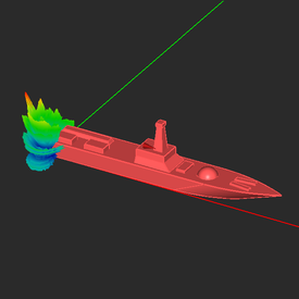
Next, visualize the 3D radiation pattern of your antenna-platform combo structure. Explore the theta and phi components of the radiation pattern, too.
The figures below show the dB-scale 2D graphs of the radiation patterns in the XY, YZ and ZX planes plotted.


