EM.Ferma Tutorial Lesson 7: Analyzing A Microstrip Transmission Line
Contents
- 1 What You Will Learn
- 2 Getting Started
- 3 A Note on Quasi-Static Solution of Transmission Line Problems
- 4 Creating the Microstrip Line Geometry
- 5 Examining the Computational Domain & the 2D Solution Plane
- 6 Running a Quasi-Static Simulation of the Microstrip Line
- 7 Verifying Your Simulation Results
- 8 Running a Parametric Sweep of the Microstrip Width
What You Will Learn
In this tutorial you will learn how to define and characterize a 2D transmission line structure like a microstrip line using quasi-static analysis. EM.Ferma provides three transmission line wizards:
- Microstrip Wizard
- CPW Wizard
- Coaxial Wizard
You will also learn how to set up and perform a parametric sweep of your design variables.
![]() Back to EM.Ferma Tutorial Gateway
Back to EM.Ferma Tutorial Gateway
![]() Download projects related to this tutorial lesson
Download projects related to this tutorial lesson
Getting Started
Open the EM.Cube application and switch to EM.Ferma. Start a new project with the following parameters:
A Note on Quasi-Static Solution of Transmission Line Problems
Most popular two-conductor transmission line types like microstrip, stripline, coplanar waveguide (CPW), etc., feature a single dominant TEM or TEM-like propagating mode. Therefore, they can be reasonably modeled using quasi-static methods. EM.Ferma takes the cross section of an infinitely long 2D transmission line structure and encloses it by a PEC domain box. Shielded transmission lines are naturally well-represented using this approach. To model open-boundary transmission lines like a microstrip line, you must place the domain boundary walls far enough from the signal line.
EM.Ferma can perform 2D electrostatic and quasi-static simulations. For this purpose, you need to define a "2D Solution Plane". The cross section of your physical structure on this 2D solution plane is taken as the geometry to be solved. In other words, EM.Ferma assumes that this cross sectional geometry is invariably extended to the infinity from both sides of the solution plane.
To compute the characteristic impedance Z0 and effective permittivity εeff of the transmission line, EM.Ferma first analyzes the structure "As Is" and finds the electric field everywhere in the computational domain. Gauss' law is used to compute the total charge on the signal line, from which the capacitance C is calculated. Then, all the dielectric parts are replaced with air (εr = 1). The electrostatic problem is solve one more time and the "air-filled" capacitance Ca is calculated. The characteristic impedance and effective permittivity of the transmission line are then calculated from the following relations:
[math] Z_0 = \frac{1}{c_0 \sqrt{CC_a} } [/math]
[math] \epsilon_{eff} = \frac{C}{C_a} [/math]
where c0 = 3×10⁸ m/s is the speed of light in the free space.
Creating the Microstrip Line Geometry
A microstrip line consists of a metallic strip printed on top of a dielectric substrate with a conductor backing on its other side. Click on the Microstrip Wizard ![]() button of the Wizard Toolbar or select the menu item Tools → Transmission Line Wizards → Microstrip Line.
button of the Wizard Toolbar or select the menu item Tools → Transmission Line Wizards → Microstrip Line.
The geometry of a microstrip line appears at the center of the project workspace.
The geometry created by the wizard consists of three objects belonging to three different material groups:
| Object Name | Object Type | Material Group Name | Material Group Type |
|---|---|---|---|
| ANCHOR | Rectangle Strip | STRIP | Fixed-potential PEC |
| Ground | Rectangle Strip | GROUND | Fixed-potential PEC |
| Substrate | Box | SUBSTRATE | Dielectric material |
Open the property dialogs of the three material groups and examine their parameters. The fixed voltage of the "STRIP" PEC group is 1V, while the fixed voltage of the "GROUND" PEC group is 0V. The geometry created by the wizard is fully parameterized. Open the variables dialog and review the list of the variables used for the definition of the microstrip line. Change the value of "strip_wid" to 4.62893mm. You will notice that the "sub_size" will change to 46.2893mm.
Open the property dialog of the rectangle strip object called "ANCHOR", which represents the metallic strip on the top side of the dielectric substrate. From the variables dialog shown above, note that the width of the transmission line has been defined as a function of another variable called "z0", which represents the characteristics impedance. The current value of z0 is 50Ω. In other words, the Y-dimension of the rectangle strip "ANCHOR" is controlled by the value you set for the variable "z0". Also note that since EM.Ferma uses the finite difference method for quasi-static analysis of 2D transmission lines, it requires a substrate of finite size. For this reason, the wizard has set the widths of the substrate and ground equal to 10 times the width of the microstrip.
Examining the Computational Domain & the 2D Solution Plane
So far in all the previous tutorial lessons, you dealt with 3D domain boxes and performed 3D electrostatic or 3D magneostatic simulations of 3D physical structures. EM.Ferma also lets you perform 2D electrostatic analysis of 2D structures. By a 2D structure we mean a geometry that is invariant along one of the three principal axes and has an infinite extent along that direction. The cross section of a 2D structure is identical at any point along the so-called invariance axis. Therefore, you can build a 3D transmission line geometry just like other structures you built earlier and then specify a "2D Solution Plane" that would capture the cross section of your transmission line geometry and would pass its mesh to the simulation engine. In EM.Ferma, 2D solution planes are defined based on existing field sensor observables. Since in EM.Ferma, a field sensor plane extends across the entire computational domain, it can also serve to capture the cross section of your transmission line geometry.
Open the domain settings dialog. You will see that the wizard has set the domain offest values in the ±X and ±Y directions equal to zero. The -Z-offset is zero, too.
Remember that all the six walls of the domain box are held at zero potential by default (due to the Dirichlet boundary condition). This means that all six walls are assumed to be fix-potential PEC surface with a fixed zero voltage. You may pick a nonzero value for the -Z-offset parameter, but this will create a redundant air region between the object "Ground" and the bottom domain wall, both of which have zero voltages. The table below lists all the domain offset values.
| Offset | Value |
|---|---|
| -X | 0 |
| +X | 0 |
| -Y | 0 |
| +Y | 0 |
| -Z | 0 |
| +Z | 20mm |
Also, note that the wizard defined a vertical X-directed field sensor observable called "FS1", which is centered at (0, 0, 0).
Running a Quasi-Static Simulation of the Microstrip Line
Open the mesh settings dialog. You will find that the wizard has set the mesh cell size to a very fine value of Δx = Δy = Δz = 0.2mm. Since the width of your microstrip is about 4.6mm, this will place 23 cells across the width of the transmission line. To get accurate results, you typically need to set a very high resolution mesh for 2D transmission line structures.
Run a quasi-static "Analysis" of your 2D transmission line structure. At the end of the simulation, the output message window reports the computed values of the characteristic impedance and effective permittivity of the transmission line:
Z0: 48.605429 Ohms
Epsilon_Effective: 1.946599
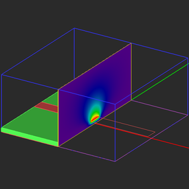
Visualize the electric field and potential distribution on the Sensor_1 plane. From the vector plot, you can clearly see the field confinement inside the dielectric substrate underneath the micrsotrip as well as the fringing fields at the edges of the metal strip.
Verifying Your Simulation Results
To verify the computed results for the characteristic impedance Z0 and εeff, let's take a look at the analytical formulas available for the characteristic impedance and effective permittivity of a microstrip line:
[math] \epsilon_{eff} = \frac{\epsilon_r + 1}{2} + \frac{\epsilon_r - 1}{2} \left( 1+ 12\frac{h}{w} \right) ^{-\frac{1}{2}} [/math]
[math] Z_0 = \frac{120\pi}{\sqrt{\epsilon_{eff}}} \left[ \frac{w}{h} + 1.393 + 0.677 ln \left( \frac{w}{h} + 1.444 \right) \right] ^{-1} [/math]
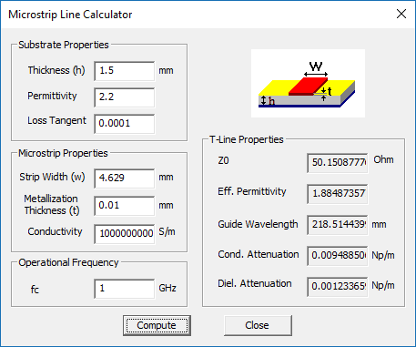
where w and h are the microstrip width and substrate thickness, respectively, and εr is the relative permittivity of the dielectric. The above formulas are valid for the case of w/h ≥ 1. For your microstrip line defined in this project, you have w = 4.7mm, h = 1.5mm and εr = 2.2. For these values, the above formulas give: Z0 = 49.54Ω and εeff = 1.87, which are not far from the simulated results.
If you have installed RF.Spice A/D on your computer, you can also produce similar results in its Device Manager. In that case, you can access the RF.Spice A/D Device Manager directly from the Tool Menu of EM.Ferma.
Running a Parametric Sweep of the Microstrip Width
You saw earlier that the variable "sub_size" was defined as a function of the variable "strip_wid". This means that "sub_size" is a dependent variable, while "strip_wid" is an independent variable. You can easily change the definition of any variable and turn it into an independent or dependent variable. Open the variable dialog and change the values of two variables "h" and "strip_wid" according to the table below:
| Variable Name | Original Definition | New Definition |
|---|---|---|
| h | 0.0015*to_meters | 1.5 |
| strip_wid | 4.62893 | 4.6 |
In this part of this tutorial lesson, you will vary the microstrip width and see how it affects the characteristic impedance and effective permitivity of your transmission line. In a sweep simulation, one or more parameters are varied, and the simulation engine is run for each parameter set. Open the Simulation Run dialog and choose the Parametric Sweep option from the Simulation Mode drop-down list. Click on the Settings button next to this drop-down list to open the Parametric Sweep Settings dialog.
The sweep variables list is initially empty.
On the left side of this dialog, you see a list of all the available independent variables. Select "strip_wid" from the left table and use the right arrow --> button to move it to the right table. Another dialog titled "Sweep Variable" opens up. You have to set the start, stop and step values of your sweep variable. By default, the sweep variable is of uniform type. Enter 3, 5, and 0.2 for the start, stop and step values, respectively. This will create a value list of {3.0, 3.2, 3.4, 3.6, 3.8, 4.0, 4.2, 4.4, 4.6, 4.8, 5.0}. Close the sweep variable dialog and then close the sweep settings dialog to return to the simulation run dialog.
Run the sweep simulation. It may take a while as a total of eleven individual 2D electrostatic simulations must be completed. At the end of the parametric sweep, open the data manager and plot the data files "SP1_Z0_Sweep.DAT" and "SP1_EpsEff_Sweep.DAT". You should see graphs like the figures below.


