| Tutorial Project: Designing Sample-And-Hold Circuits
|
|
|
Objective: In this project, you will build several sample-and-hold circuits using switching devices.
|
|
Concepts/Features:
- Analog Switch
- Sampling
- Sample-and-Hold Circuit
- FET Switch
- Operational Amplifier
- Voltage Follower
|
|
Minimum Version Required: All versions
|
|
' Download Link: Mixed-Signal Lesson 4 Download Link: Mixed-Signal Lesson 4
|
What You Will Learn
In this tutorial you will use SPICE's standard voltage-controlled switch as well as a semiconductor FET switch to sample signals and build sample-and-hold (S/H) circuits.
Using the Voltage-Controlled Switch to Sampling Signals
The following is a list of parts needed for this part of the tutorial lesson:
|
|
| Part Name
|
Part Type
|
Part Value
|
| VS
|
Voltage Source
|
Waveform TBD
|
| VC
|
Voltage Source
|
Waveform TBD
|
| RS
|
Resistor
|
1k
|
| RL
|
Resistor
|
5k
|
| S1
|
Voltage-Controlled Switch
|
Defaults
|
| VIN
|
Voltage Probe Marker
|
N/A
|
| VOUT
|
Voltage Probe Marker
|
N/A
|
| VCTRL
|
Voltage Probe Marker
|
N/A
|
The voltage-controlled switch with the keyboard shortcut S is a two-pin device, whose ON and OFF states are controlled by an external voltage defined in the switch's property dialog. VS is the signal source with a sinusoidal waveform. VC is the control source with a pulse waveform, which will control the opening and closing of the switch S1. Open the property dialog of the switch and set its On Voltage and Off Voltage to 4.5V and 0.1V, respectively. These are the threshold values for the control voltage. Set the On Resistance and Off Resistance values of the switch to 1u and 1G, respectively. Finally, set the Controlling Voltage by choosing "VC" from the drop-down box labeled "Voltage across part".
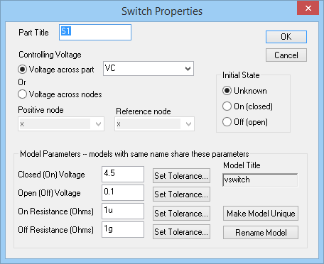 The property dialog of the voltage-controlled switch. |
 |
Always set a nonzero value for the On Resistance of the switch. Otherwise, a zero resistance may lead to simulation failure.
|
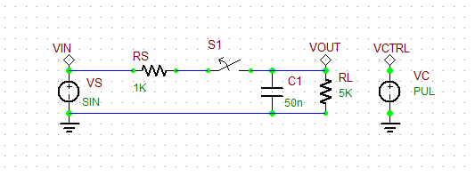
Place and connect all the parts as shown in the figure below:
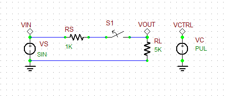 A simple sampling circuit using a voltage-controlled switch. |
Set the waveforms of the two voltage source VS and VC as specified below:
|
|
VS
| Offset Voltage
|
0
|
| Peak Amplitude
|
5
|
| Frequency
|
1k
|
| Delay Time
|
0
|
| Damping Factor
|
0
|
|
|
|
VC
| Initial Voltage
|
0
|
| Peak Voltage
|
1
|
| Delay Time
|
0
|
| Rise Time
|
1p
|
| Fall Time
|
1p
|
| Pulse Width
|
1m
|
| Pulse Period
|
3m
|
Run a Transient Test of this circuit with the parameters specified below:
|
|
| Start Time
|
0
|
| Stop Time
|
5m
|
| Linearize Step
|
1u
|
| Step Ceiling
|
1u
|
| Preset Graph Plots
|
v(VIN), v(VOUT), v(VCTRL)
|
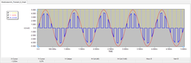
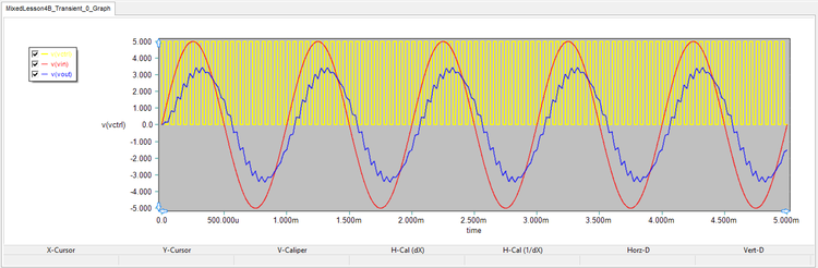
The results are shown in the figure below. As you can see from the figure, every 3ms the switch closes for a duration of 1ms, and the source voltage is transferred to the resistive load through the voltage divider. Your sinusoidal input signal is clearly under-sampled.
 The input, control and output voltages of the sampling circuit with a sampling period of 3ms. |
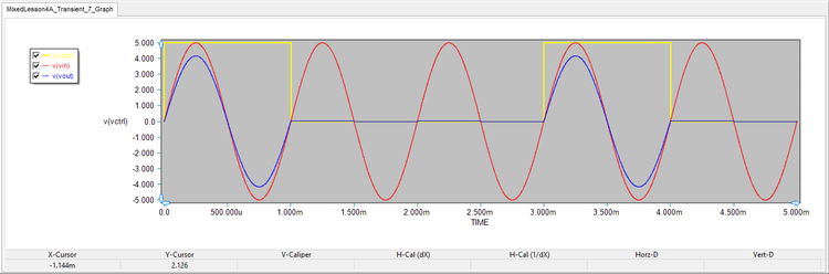
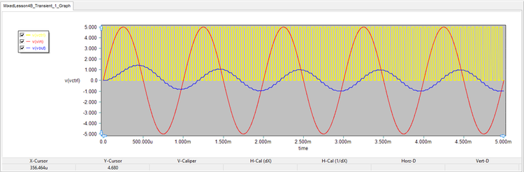
Next, change the period and pulse width of the control source according to the table below. Run another transient test with the same parameters. You can see from the figure below that each period of your is sinusoidal input signal is sampled 10 times.
|
|
VC
| Initial Voltage
|
0
|
| Peak Voltage
|
1
|
| Delay Time
|
0
|
| Rise Time
|
1p
|
| Fall Time
|
1p
|
| Pulse Width
|
50u
|
| Pulse Period
|
150u
|
 The input, control and output voltages of the sampling circuit with a sampling period of 150μs. |
Building a Basic Sample-And-Hold Circuit
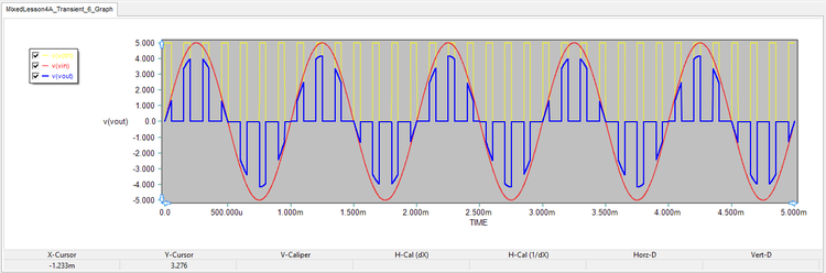
Adding a shunt capacitor C1 to the load of your sampling circuit above will make a basic sample-and-hold circuit as shown in the figure below. During the ON state of the switch (Sample Time), the capacitor C will charge to the sampled voltage value. During the OFF state of the switch (Hold Time), the capacitor will keep its held sample voltage until the next charging period. Set the capacitance initially to C1 = 50nF.
 A basic sample-and-hold circuit using a voltage-controlled switch. |
Change the control pulse waveform according to the table below:
|
|
VC
| Initial Voltage
|
0
|
| Peak Voltage
|
1
|
| Delay Time
|
0
|
| Rise Time
|
1p
|
| Fall Time
|
1p
|
| Pulse Width
|
25p
|
| Pulse Period
|
50p
|
Run a Transient Test of this circuit with the parameters specified below:
|
|
| Start Time
|
0
|
| Stop Time
|
5m
|
| Linearize Step
|
1u
|
| Step Ceiling
|
1u
|
| Preset Graph Plots
|
v(VIN), v(VOUT), v(VCTRL)
|
As you can see from this figure, the capacitor discharges too quickly during the hold time and certainly is not able to hold the sampled voltage for the entire time. Note that the time constant of this circuit is τ = RLC1 = 250μs. Of the 50μs period of the pulse waveform, the first 25μs is the sample time, and the remaining 25μs is the hold time. Clearly, the discharge time constant is too short.
 The input, control and output voltages of the basic S/H circuit with C1 = 50nF. |
Next, increase the value of C1 to 400nF. In this case, the discharge time constant will increase to τ = 2ms. Run a new transient test of the circuit with the same parameters as before, and you will get the results shown in the figure below. You can see an improvement of the performance of your S/H circuit but in exchange for lower amplitude and larger delay time.
 The input, control and output voltages of the basic S/H circuit with C1 = 400nF. |
Building an Op-Amp Sample-And-Hold Circuit
The following is a list of parts needed for this part of the tutorial lesson:
|
|
| Part Name
|
Part Type
|
Part Value
|
| VS
|
Voltage Source
|
Waveform TBD
|
| VC
|
Voltage Source
|
Waveform TBD
|
| C1
|
Capacitor
|
1n
|
| D1
|
Generic Diode
|
Defaults
|
| J1
|
Generic N-Type JFET
|
Defaults
|
| Vcc
|
DC Bias Voltage Source
|
15V
|
| Vee
|
DC Bias Voltage Source
|
-15V
|
| X1 - X2
|
AD711 Op-Amp
|
Defaults
|
| VIN
|
Voltage Probe Marker
|
N/A
|
| VOUT
|
Voltage Probe Marker
|
N/A
|
| VCTRL
|
Voltage Probe Marker
|
N/A
|
Configure the two Op-Amps as voltage followers acting as buffers between the input and output as shown in the figure below. The JFET transistor J1 acts as the switch which turns on and off by the control voltage applied to its gate. The shunt charge capacitor is connected between the output of the switch and the input of the second voltage follower.
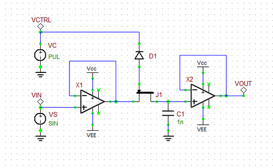 A sample-and-hold circuit with Op-Amps and a FET Switch. |
Set the waveforms of the two voltage sources VS and VC as specified below:
|
|
VS
| Offset Voltage
|
0
|
| Peak Amplitude
|
5
|
| Frequency
|
1k
|
| Delay Time
|
0
|
| Damping Factor
|
0
|
|
|
|
VC
| Initial Voltage
|
0
|
| Peak Voltage
|
1
|
| Delay Time
|
0
|
| Rise Time
|
1p
|
| Fall Time
|
1p
|
| Pulse Width
|
5u
|
| Pulse Period
|
50u
|
Run a Transient Test of this circuit with the parameters specified below:
|
|
| Start Time
|
0
|
| Stop Time
|
5m
|
| Linearize Step
|
1u
|
| Step Ceiling
|
1u
|
| Preset Graph Plots
|
v(VIN), v(VOUT), v(VCTRL)
|
The simulation results are shown in the figure below. As you can see from the graph, the Op-Amp S/H circuit performs much better than the basic S/H circuit of the previous part and does not introduce any delay or attenuation to the output signal.
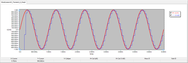 The input, control and output voltages of the Op-Amp S/H circuit with C1 = 1nF. |
 Back to RF.Spice A/D Tutorial Gateway Back to RF.Spice A/D Tutorial Gateway
|
|
|
|


