The Very Old Glossary of Black-Box Spectral Processing & Modulation Virtual Blocks
Contents
- 1 Amplitude Modulator Block
- 2 Amplitude Shift-Keying Modulator Block
- 3 Analog One-Half Frequency Divider Block
- 4 Analog Phase-Locked Loop Block
- 5 Delta Modulator Block
- 6 Delta-Sigma Modulator Block
- 7 Differential Phase Shift-Keying Modulator Block
- 8 Frequency Doubler Block
- 9 Frequency Down-Converter Block
- 10 Frequency Modulator Block
- 11 Frequency Shift-Keying Modulator Block
- 12 Frequency Up-Converter Block
- 13 Generalized Analog Filter Block
- 14 Generic Bandpass Filter Block
- 15 Generic Bandstop Filter Block
- 16 Generic Highpass Filter Block
- 17 Generic Lowpass Filter Block
- 18 Phase Modulator Block
- 19 Phase Shift-Keying Modulator Block
- 20 Pulse Width Modulator Block
- 21 Quadrature Amplitude Modulator Block
- 22 Sine Wave VCO Block
- 23 Square Wave VCO Block
- 24 Triangular Wave VCO Block
- 25 xN Frequency Multiplier Block
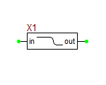
Amplitude Modulator Block
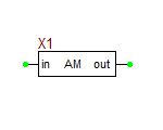
This device takes an input signal and generates an AM modulated output signal of a specified carrier frequency with a specified modulation index.
Parameters:
| NAME | PARAMETER | UNITS | DEFAULT | NOTES |
|---|---|---|---|---|
| r_in | input resistance | Ω | 1G | |
| r_out | output resistance | Ω | 1u | |
| m | modulation index | - | 0.5 | |
| fc | carrier frequency | Hz | 1Meg | |
| ac | carrier peak amplitude | V | 1 |
Amplitude Shift-Keying Modulator Block
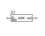
This device takes a digital input like a binary sequence and generates an ASK modulated output signal with two specified carrier amplitude levels.
Parameters:
| NAME | PARAMETER | UNITS | DEFAULT | NOTES |
|---|---|---|---|---|
| r_out | output resistance | Ω | 1u | |
| fc | carrier frequency | Hz | 1Meg | |
| ac_lo | low carrier peak amplitude | V | 0.0 | |
| ac_hi | high carrier peak amplitude | V | 1.0 |
Analog One-Half Frequency Divider Block
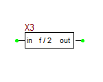
This device takes a harmonic input signal and generates a harmonic output signal with a frequency one half lower and a user specified amplitude.
Parameters:
| NAME | PARAMETER | UNITS | DEFAULT | NOTES |
|---|---|---|---|---|
| r_in | input resistance | Ω | 1G | |
| r_out | output resistance | Ω | 1u | |
| max_val | output amplitude | V | 1.0 |
Analog Phase-Locked Loop Block
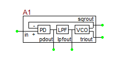
This 5-pin device is a parameterized model of an analog phase-locked loop. It provides two phase-locked output signals with square wave and triangular wave waveforms. The outputs of the lowpass filter and phase detector are also accessible via the designated pins.
Parameters:
| NAME | PARAMETER | UNITS | DEFAULT | NOTES |
|---|---|---|---|---|
| r_in | input resistance | Ω | 1G | |
| r_out | output resistance | Ω | 1u | |
| K_d | voltage conversion factor of phase detector | V/rad | 1.0 | |
| K_f | frequency conversion factor of VCO | Hz/V | 1k | |
| V_sq | square wave output peak amplitude | V | 1 | |
| V_tri | triangular wave output peak amplitude | V | 1 | |
| VT | VCO input dynamic range | V | 1 | |
| r_time | VCO timing resistor | Ω | 12k | |
| c_time | VCO timing capacitor | F | 10n | |
| fo | VCO free-running frequency | Hz | 1k | |
| r_lpf | lowpass filter resistor | Ω | 10k | |
| c_lpf | lowpass filter capacitor | F | 100n |
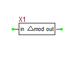
Delta Modulator Block
This device samples an input signal at the specified sampling period and generates a Delta modulated output signal from it.
Parameters:
| NAME | PARAMETER | UNITS | DEFAULT | NOTES |
|---|---|---|---|---|
| r_in | input resistance | Ω | 1G | |
| r_out | output resistance | Ω | 1u | |
| T | sampling period | sec | 1 | |
| duty_cycle | sampling pulse duty cycle | - | 0.01 |
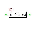
Delta-Sigma Modulator Block
This device samples an input signal at the specified sampling period and generates a Delta-Sigma modulated output signal from it.
Parameters:
| NAME | PARAMETER | UNITS | DEFAULT | NOTES |
|---|---|---|---|---|
| r_in | input resistance | Ω | 1G | |
| r_out | output resistance | Ω | 1u | |
| T | sampling period | sec | 1 | |
| duty_cycle | sampling pulse duty cycle | - | 0.01 |
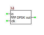
Differential Phase Shift-Keying Modulator Block
This device takes a digital input like a binary sequence and generates a DPSK modulated output signal with two specified carrier phase values. It also requires a digital clock input for synchronization.
Parameters:
| NAME | PARAMETER | UNITS | DEFAULT | NOTES |
|---|---|---|---|---|
| r_out | output resistance | Ω | 1u | |
| phi_lo | low carrier phase value | rad | 0 | |
| phi_hi | high carrier phase value | rad | π | |
| fc | carrier frequency | Hz | 1Meg | |
| ac | carrier peak amplitude | V | 1.0 |
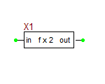
Frequency Doubler Block
This device takes a harmonic input signal and generates a harmonic output signal with twice the frequency and a user specified amplitude.
Parameters:
| NAME | PARAMETER | UNITS | DEFAULT | NOTES |
|---|---|---|---|---|
| r_in | input resistance | Ω | 1G | |
| r_out | output resistance | Ω | 1u | |
| max_val | output amplitude | V | 1.0 |
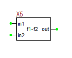
Frequency Down-Converter Block
This 3-pin device takes two harmonic input signals with different frequencies fLO and fIF and generates a harmonic output signal with a frequency equal to fRF = fLO - fIF and a user specified amplitude.
Parameters:
| NAME | PARAMETER | UNITS | DEFAULT | NOTES |
|---|---|---|---|---|
| r_in | input resistance | Ω | 1G | |
| r_out | output resistance | Ω | 1u | |
| max_in | peak amplitude of both inputs | V | 1.0 | Both inputs must have equal amplitudes. |
| max_out | output amplitude | V | 1.0 |
Frequency Modulator Block
This device takes an input signal and generates an FM modulated output signal of a specified carrier frequency with a specified maximum frequency deviation.
Parameters:
| NAME | PARAMETER | UNITS | DEFAULT | NOTES |
|---|---|---|---|---|
| r_in | input resistance | Ω | 1G | |
| r_out | output resistance | Ω | 1u | |
| f_del | maximum frequency deviation | Hz | 500k | |
| fc | carrier frequency | Hz | 1Meg | |
| ac | carrier peak amplitude | V | 1 |
Frequency Shift-Keying Modulator Block
This device takes a digital input like a binary sequence and generates an FSK modulated output signal with two specified carrier frequencies.
Parameters:
| NAME | PARAMETER | UNITS | DEFAULT | NOTES |
|---|---|---|---|---|
| r_out | output resistance | Ω | 1u | |
| fc_lo | low carrier frequency | Hz | 1Meg | |
| fc_hi | high carrier frequency | Hz | 2Meg | |
| ac | carrier peak amplitude | V | 1.0 |
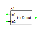
Frequency Up-Converter Block
This 3-pin device takes two harmonic input signals with different frequencies fLO and fIF and generates a harmonic output signal with a frequency equal to fRF = fLO + fIF and a user specified amplitude.
Parameters:
| NAME | PARAMETER | UNITS | DEFAULT | NOTES |
|---|---|---|---|---|
| r_in | input resistance | Ω | 1G | |
| r_out | output resistance | Ω | 1u | |
| max_in | peak amplitude of both inputs | V | 1.0 | both inputs must have equal amplitudes. |
| max_out | output amplitude | V | 1.0 |
Generalized Analog Filter Block
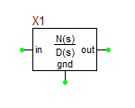
This block models a generalize analog filter characterized by a rational transfer functions in the spectral domain Laplace variable s:
[math] H(s) = \frac{N(s)}{D(s)} = \frac{ \sum_{m=0}^{M} b_m s^m }{ \sum_{n=0}^{N} a_n s^n } [/math]
subject to the requirement N ≥ M and aN = 1. To access the parameters of this block, you have to click the Edit Model... button of its property dialog.
The functionality of this block, which is native to RF.Spice A/D, is very similar to the s-domain transfer function block, which is an XPSICE process model. This block does not have a denormalization frequency parameter. Therefore, at frequencies other than the unit frequency, the transfer function must be explicitly scaled. This block can be used in conjunction with both transient and AC frequency sweep tests.
Parameters:
| NAME | PARAMETER | UNITS | DEFAULT | NOTES |
|---|---|---|---|---|
| deg | highest degree of s in transfer function | - | 2 | required |
| coeff_den | denominator coefficients array: coefficients of powers of s, highest power first | - | 1 0 1 | required |
| coeff_num | numerator coefficients array: coefficients of powers of s, highest power first | - | 0 0 1 | required |
| r_in | input resistance | Ω | 10G | |
| r_out | output resistance | Ω | 1u |
Generic Bandpass Filter Block
This device is a generic bandpass filter with user specified center frequency and bandwidth. It is based on a fifth-order Butterworth LC ladder topology.
Parameters:
| NAME | PARAMETER | UNITS | DEFAULT | NOTES |
|---|---|---|---|---|
| f0 | center frequency | Hz | 1Meg | |
| bw | bandwidth | Hz | 200k | |
| r0 | source/load resistance | Ω | 50 |
Generic Bandstop Filter Block
This device is a generic bandstop filter with user specified center frequency and bandwidth. It is based on a fifth-order Butterworth LC ladder topology.
Parameters:
| NAME | PARAMETER | UNITS | DEFAULT | NOTES |
|---|---|---|---|---|
| f0 | center frequency | Hz | 1Meg | |
| bw | bandwidth | Hz | 200k | |
| r0 | source/load resistance | Ω | 50 |
Generic Highpass Filter Block
This device is a generic highpass filter with a user specified cutoff frequency. It is based on a fifth-order Butterworth LC ladder topology.
Parameters:
| NAME | PARAMETER | UNITS | DEFAULT | NOTES |
|---|---|---|---|---|
| cutoff | cutoff frequency | Hz | 1Meg | |
| r0 | source/load resistance | Ω | 50 |
Generic Lowpass Filter Block
This device is a generic lowpass filter with a user specified cutoff frequency. It is based on a fifth-order Butterworth LC ladder topology.
| NAME | PARAMETER | UNITS | DEFAULT | NOTES |
|---|---|---|---|---|
| cutoff | cutoff frequency | Hz | 1Meg | |
| r0 | source/load resistance | Ω | 50 |
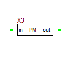
Phase Modulator Block
This device takes an input signal and generates an PM modulated output signal of a specified carrier frequency with a specified maximum phase deviation.
Parameters:
| NAME | PARAMETER | UNITS | DEFAULT | NOTES |
|---|---|---|---|---|
| r_in | input resistance | Ω | 1G | |
| r_out | output resistance | Ω | 1u | |
| phi_del | maximum phase deviation | rad | π | |
| fc | carrier frequency | Hz | 1Meg | |
| ac | carrier peak amplitude | V | 1 | |
| phi0 | carrier phase | rad | 0 |
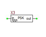
Phase Shift-Keying Modulator Block
This device takes a digital input like a binary sequence and generates a PSK modulated output signal with two specified carrier phase values.
Parameters:
| NAME | PARAMETER | UNITS | DEFAULT | NOTES |
|---|---|---|---|---|
| r_out | output resistance | Ω | 1u | |
| phi_lo | low carrier phase value | rad | 0 | |
| phi_hi | high carrier phase value | rad | π | |
| fc | carrier frequency | Hz | 1Meg | |
| ac | carrier peak amplitude | V | 1.0 |
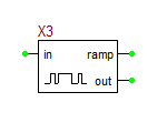
Pulse Width Modulator Block
This device takes an input signal and compares it to an internally generated ramp signal with a specified period and generates a binary PWM modulated output signal. A designated pin provides the ramp signal output.
Parameters:
| NAME | PARAMETER | UNITS | DEFAULT | NOTES |
|---|---|---|---|---|
| r_in | input resistance | Ω | 1G | |
| r_out | output resistance | Ω | 1u | |
| V_lo | low output voltage level | V | 0 | |
| V_hi | high output voltage level | V | 1 | |
| V_lo | hysteresis voltage tolerance | V | 100m | |
| T_rmp | sampling period | sec | 1m | |
| rmp_lo | ramp minimum voltage level | V | 0 | |
| rmp_hi | ramp maximum voltage level | V | 1 | |
| duty_cycle | ramp duty cycle | - | 0.01 | Must be between 0.01 and 0.99 |
Quadrature Amplitude Modulator Block
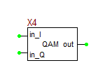
This 3-pin device takes two input signals and generates a QAM modulated output signal of a specified carrier frequency:
[math] v_{out}(t) = A_c \left( v_{in_I}(t) \cdot \cos(2\pi f_c t) + v_{in_Q}(t) \cdot \sin(2\pi f_c t) \right) [/math]
Parameters:
| NAME | PARAMETER | UNITS | DEFAULT | NOTES |
|---|---|---|---|---|
| r_in | input resistance | Ω | 1G | |
| r_out | output resistance | Ω | 1u | |
| fc | carrier frequency | Hz | 1Meg | |
| ac | carrier peak amplitude | V | 1 |
Sine Wave VCO Block
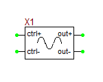
This device is a voltage-controlled oscillator block with a sinusoidal output signal.
Parameters:
| NAME | PARAMETER | UNITS | DEFAULT | NOTES |
|---|---|---|---|---|
| fo | free-running frequency | Hz | 1Meg | |
| K_f | frequency conversion factor | Hz/V | 500k | |
| max_val | output peak amplitude | V | 1 |
Square Wave VCO Block
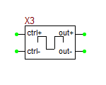
This device is a voltage-controlled oscillator block with a square wave output signal oscillating between two binary voltage levels.
Parameters:
| NAME | PARAMETER | UNITS | DEFAULT | NOTES |
|---|---|---|---|---|
| fo | free-running frequency | Hz | 1Meg | |
| K_f | frequency conversion factor | Hz/V | 500k | |
| duty_cycle | pulse duty cycle | - | 0.5 | |
| rise_time | pulse rise time | sec | 1n | |
| fall_time | pulse fall time | sec | 1n | |
| out_low | output lower limit | V | -1.0 | |
| out_high | output higher limit | V | -1.0 |
Triangular Wave VCO Block
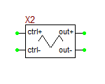
This device is a voltage-controlled oscillator block with a triangular wave output signal oscillating between two binary voltage levels. The parameter "duty_cycle" has a default value of 0.5, generating a symmetric triangular output. In the limiting cases of duty_cycle = 0.99 and duty_cycle = 0.01, the output will have an up-ramp or a down-ramp sawtooth waveform, respectively.
Parameters:
| NAME | PARAMETER | UNITS | DEFAULT | NOTES |
|---|---|---|---|---|
| fo | free-running frequency | Hz | 1Meg | |
| K_f | frequency conversion factor | Hz/V | 500k | |
| duty_cycle | triangular waveform duty cycle | - | 0.5 | Must be between 0.01 and 0.99. |
| out_low | output lower limit | V | -1.0 | |
| out_high | output higher limit | V | -1.0 |
xN Frequency Multiplier Block
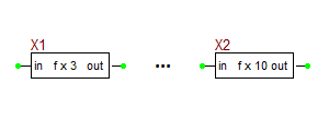
These devices take a harmonic input signal and generate a harmonic output signal with a frequency N times larger and a user specified amplitude: N = 3, 4, 5, 6, 7, 8, 9, 10.
Parameters:
| NAME | PARAMETER | UNITS | DEFAULT | NOTES |
|---|---|---|---|---|
| r_in | input resistance | Ω | 1G | |
| r_out | output resistance | Ω | 1u | |
| max_val | output amplitude | V | 1.0 |
