Designing a Distributed Bandpass Filter Using Coupled Lines
Objective
In this tutorial, first you will learn about RF.Spice's Generic Couple T-Lines model. Then you will cascade several sections of coupled T-Lines to design a distributed bandpas filter. Finally, you will realize a microstrip version of your distributed bandpass filter.
The Generic Coupled T-Lines Device
RF.Spice's Generic Couple T-Lines can be accessed from the Schematic Editor's RF Menu. It is a four-port device that models two parallel transmission line segments with equal lengths. Coupled line have several applications in RF circuit design including directional couplers, hybrids and filters. Normally you would the positive pins of the four ports and ground all the four negative pins. In RF.Spice, the generic coupled T-line device is characterized by its even and odd mode impedances, Z0e and Z0o. The system characteristic impedance of the device is defined as the geometric mean of these two impedances: Z0s = √(Z0eZ0o). Even though real physical coupled line structures have slightly different effective permittivities, the average of these two is usually taken as the effective permittivity of overall transmission line. The opposite figure shows the property dialog of the Generic Coupled T-Lines device.
Exciting the Even and Odd Modes of Coupled Lines
The following is a list of parts needed for this part of the tutorial lesson:
Two AC Voltage Sources: VS1 and VS2 (keyboard shortcut: Alt+V)
A Generic Coupled T-Line: Accessible from RF Menu
Four 50Ω Resistors: RS1, RS2, RL1 and RL2 (keyboard shortcut: R)
Two Voltage Probe Markers: VP1 and VP2 (keyboard shortcut: Alt+L)
In the analysis of coupled transmission lines, it is customary to decompose signals as the superposition of two orthogonal modes: the even and odd modes. In this part of the tutorial lesson, you will excite each of these modes. Set the values of the even and odd mode impedances of the coupled lines to Z0e = 70Ω and Z0o = 30Ω, respectively. Set the length of the lines to len = 37.5mm, which is a quarter wavelength at 2GHz assuming TEM lines (eeff = 1).
First, you will excite the even mode. Connect the two voltage sources VS1 and VS2 through the source resistors RS1 and RS2 to the positive pins of Port 1 and Port 3 of the coupled lines device, respectively. Connect the two load resistors RL1 and RL3 to the positive pins of Port 2 and Port 4 of the coupled lines device, respectively. Place voltage probe markers VP1 and VP2 at Ports 1 and 3, respectively. Run an AC Sweep Test of this circuit. Set the start and stop frequencies of the sweep to 500MHz and 3.5GHz, respectively, with a linear frequency step size of 10MHz. In the AC Sweep Test Panel, check both "Graph" and "Table" checkboxes.
After the completion of the AC sweep, you should get a voltage graph and data table similar to the ones shown below. Note from the real/imag parts table that the two input voltages are equal.
Next, you will excite the odd mode. In this case, you will connect just a single voltage source VS1 in series with the source resistor RS1 between the positive pins of Port 1 and Port 3 of the coupled lines device as shown in the opposite figure. Connect the two load resistors RL1 and RL3 to the positive pins of Port 2 and Port 4 of the coupled lines device, respectively. Place voltage probes VP1 and VP2 at Ports 1 and 3, respectively. Run an AC Sweep Test of this circuit with the same sweep settings as in the previous case. After the completion of the AC sweep, you should get a voltage graph and data table similar to the ones shown below. This time, from the real/imag parts table you can see that the two input voltages are 180° out of phase.
Coupled Line Analysis
The Generic Coupled T-Lines device is a four-port device that can easily be analyzed based on its impedance (Z) parameters. Consider the four-port being driven from Ports 1 and 3 in the even mode, with Ports 2 and 4 terminated in two identical loads ZL. The voltage at any point on either T-Line segment can be expressed as:
[math]V_1(z) = V_2(z) = V_e^+ \left[ e^{-j\beta (z-L)} + \Gamma_{L}^e e^{j\beta (z-L)} \right] [/math]
where Ve+ is a constant, the coordinate z = 0 is assumed to be the location of Ports 1 and 3, and ΓLe is the load reflection coefficient for the even mode case:
[math]\Gamma_L^e = \frac{Z_L - Z_{0e}}{Z_L + Z_{0e}}[/math]
The input voltages VP1 and VP2 in the even mode can now be written as:
[math]V_{P1} = V_1(z=0) = V_{P2} = V_2(z=0) = V_e^+ e^{j\beta L} \left[ 1 + \Gamma_{L}^e e^{-2j\beta L} \right] [/math]
Now, let's drive the four-port from Ports 1 and 3 in the odd mode. The voltage at any point on either T-Line segment in this case can be expressed as:
[math]V_1(z) = -V_2(z) = V_o^+ \left[ e^{-j\beta z} + \Gamma_{L}^o e^{j\beta z} \right] [/math]
where Vo+ is another constant, and ΓLo is the load reflection coefficient for the odd mode case:
[math]\Gamma_L^o = \frac{Z_L - Z_{0o}}{Z_L + Z_{0o}}[/math]
The input voltages VP1 and VP2 in the odd mode can now be written as:
[math]V_{P1} = V_1(z=0) = -V_{P2} = -V_2(z=0) = V_o^+ e^{j\beta L} \left[ 1 + \Gamma_{L}^o e^{-2j\beta L} \right] [/math]
The above results can clearly be observed on the voltage graphs of the previous part, which exhibit a standing wave pattern. Note that in this case, ΓLe = (50-70)/(50+70) = -0.167 and ΓLo = (50-30)/(50+30) = 0.25. As you already saw in Tutorial Lesson 1, the exponent βL = 2πL/λg = 2π√(εeff)(f.L)/c determines the frequency variation of the voltage.
For Z-parameter calculations, we open-circuit Ports 2 and 4 (ZL = ∞). In this case, ΓLe = ΓLo = 1, and the voltages at Ports 1 and 3 now reduce to:
[math]v_1^e(0) = v_2^e(0) = 2V_e^+ cos(\beta L) = i_e Z_{in}^e [/math]
[math]v_1^o(0) = -v_2^o(0) = 2V_o^+ cos(\beta L) = i_o Z_{in}^o [/math]
where ie and io are the even and odd current at Ports 1 and 3, respectively. The total currents at Ports 1 and 3 can be expressed as (ie + io) and (ie - io), respectively. Moreover, the input impedances seen at Ports 1 and 3 in the case of even and odd excitations are given by:
[math]Z_{in}^e = -jZ_{0e} cot( \beta L) [/math]
[math]Z_{in}^o = -jZ_{0o} cot( \beta L) [/math]
Similar equations can be derived for Ports 2 and 4, when Ports 1 and 3 are open-circuited. From all these equations, one can relate the open-circuit port voltages to the port currents and finally derive the Z matrix of the four-port as follows:
where ZS = (Z0e + Z0o)/2 and ZD = (Z0e - Z0o)/2.
Examining the Filter Building Blocks
A two-port network can be formed by terminating two of the four ports of a Generic Coupled T-Lines device in either short or open circuits. Several configurations are possible. You can then build narrowband bandpass filters by cascading several of such terminated coupled transmission line segments. For this project, you will open-circuit Ports 2 and 3 of the Generic Coupled T-Lines device and will use Port 1 and Port 4 as the input and output ports of the resulting two-port network, respectively. This is shown in the opposite figure. In this case, the 4×4 Z matrix is reduced to a 2×2 matrix with the following elements:
[math]Z_{11} = Z_{22} = -\frac{j}{2} \left( Z_{0e} + Z_{0o} \right) cot \left( \frac{2\pi f}{c} L \sqrt{\epsilon_{eff}} \right) [/math]
[math]Z_{21} = Z_{12} = -\frac{j}{2} \left( Z_{0e} - Z_{0o} \right) csc \left( \frac{2\pi f}{c} L \sqrt{\epsilon_{eff}} \right) [/math]
Build a new circuit using a Generic Coupled T-Lines device with Z0e = 70Ω, Z0o =30Ω and len = 37.5mm. Use two Net Markers to designate the input and output ports. Run a Network Analysis Test of your circuit with start and stop sweep frequencies set to 1GHz and 3GHz, respectively, and a linear frequency step size of 1GHz. Check only the "Table" checkbox and uncheck the "Graph" checkbox. In the "Output" tab of Network Analysis Test Panel, choose "Z" Parameters options with "Real/Imag" format. Make sure to uncheck the "Decibels" checkbox. The simulated Z-parameter results are compared to their analytical values in the table below:
| f | βL | Analytical Z11 [Ω] | Simulated Z11 [Ω] | Analytical Z21 [Ω] | Simulated Z21 [Ω] |
|---|---|---|---|---|---|
| 1GHz | π/4 | -j50 | 0.009 - j50 | -j28.284 | 0.003 - j28.284 |
| 2GHz | π/2 | 0.003 | 0 | -j20 | - j20 |
| 3GHz | 3π/4 | j50 | 0.009 + j50 | -j28.284 | -0.003 - j28.284 |
Before closing this section, run another Network Analysis Test of your circuit with the same port assignments. But this time you will calculate the S-parameters over a wider frequency range from 500MHz to 3.5GHz with a linear frequency step size of 10MHz. Choose the "S" Parameters option with Amplitude-Only Cartesian graph type. Check the "Decibels" checkbox once again. The insertion loss (|s21|) and return loss (|s11|) results are shown in the figure below:
Designing a Coupled Line Bandpass Filter
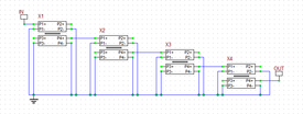
In this part of the tutorial lesson you will cascade four quarter-wavelength Generic Coupled T-Line segments to build a distributed bandpass filter as shown in the opposite figure. Port 1 of the first segment and Port 4 of the last segment are designated as the input and output ports. Port 4 of each segment is fed into Port 1 of the next segment. Ports 2 and 3 of all coupled line devices are left open-circuited. Proper grounding is done for all the negative pins.
The following table gives the parameters of each segment:
| Coupled Line Segment | Z0e | Z0o | eeff | len |
|---|---|---|---|---|
| L1 | 70.61Ω | 39.24Ω | 1 | 37.5mm |
| L2 | 56.64Ω | 44.77Ω | 1 | 37.5mm |
| L3 | 56.64Ω | 44.77Ω | 1 | 37.5mm |
| L4 | 70.61Ω | 39.24Ω | 1 | 37.5mm |
All the segment lengths are chose to be len = 37.5mm, which is a quarter wavelength at the center frequency of the filter fo = 2GHz. TEM transmission lines with εeff = 1 are assumed. The impedances have been chosen to achieve an equal-ripple bandpass filter design.
Run a network analysis of this two-port circuit. Set the start and stop frequency of the sweep to 1GHz and 3GHz, respectively, with a linear step of 10MHz. Generate an amplitude-only, Cartesian graph of the S-parameters. The figure below shows the graph of s11- and s21 parameters. Note that a linear scale is used for frequency. The filter has a center frequency of fo = 2GHz with a 3dB bandwidth of about 235MHz. The response drops to -45dB at 1.5GHz and 2.5GHz.
Realizing a Microstrip Version of the Coupled Line Bandpass Filter
In the last part of this tutorial lesson, you will design and test a microstrip realization of the coupled line bandpass filter you simulated in the previous part. For this purpose, you will use a substrate of thickness h = 1.6mm with εeff = 3.4. You will assume a lossless substrate (tand = 0). Remember that in the previous section, TEM line segments with εeff = 1 were assumed and the length of the coupled line segments were set to be a quarter free-space wavelength at 2GHz. For this part, first you need to design couple microstrip lines with the given even and odd mode impedances. Then, you have to calculate the guide wavelengths of the couple microstrips at 2GHz. You will do these using RF.Spice's Device Editor.
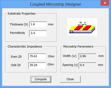
Open the "Coupled Microstrips Designer" dialog from the RF Menu of Device Editor. Enter the substrate parameters: h = 1.6mm and er = 3.4. Enter the Z0e and Z0o values for the two types of coupled line segments from the previous section and calculate width and spacing of the coupled microstrip lines for each case. Then, open the "Coupled Microstrips Calculator" dialog from the RF Menu of Device Editor. Enter the calculated microstrip width and spacing values to verify your design and also find the corresponding guide wavelengths λg at 2GHz. The lengths of the coupled microstrip segments are chosen to be a quarter of the corresponding guide wavelength at 2GHz. The following table summarizes the parameters of the coupled microstrip segments L1, L2, L3 and L4.
| Coupled Microstrip Segment | Z0e | Z0o | w | s | Average εeff | λg at 2GHz | len |
|---|---|---|---|---|---|---|---|
| L1 | 70.61Ω | 39.24Ω | 2.96mm | 0.4mm | 2.57 | 93.52mm | 23.38mm |
| L2 | 56.64Ω | 44.77Ω | 3.6mm | 1.68mm | 2.66 | 91.97mm | 23mm |
| L3 | 56.64Ω | 44.77Ω | 3.6mm | 1.68mm | 2.66 | 91.97mm | 23mm |
| L4 | 70.61Ω | 39.24Ω | 2.96mm | 0.4mm | 2.57 | 93.52mm | 23.38mm |
Build your microstrip circuit using four "Coupled Mirostrips" parts with the parameters specified in the above table. Connect them in a cascade fashion as shown in the opposite figure. Run a network analysis of this two-port circuit. Set the start and stop frequency of the sweep to 1GHz and 3GHz, respectively, with a linear step of 10MHz. Generate an amplitude-only, Cartesian graph of the S-parameters. The graphs of s11- and s21 parameters are shown in the figure below and agree perfectly with the results of the previous section.


