Difference between revisions of "RF Tutorial Lesson 11: Designing a Microstrip MESFET Amplifier"
Kazem Sabet (Talk | contribs) (Created page with "{{projectinfo|Tutorial| Analyzing Distributed RF Amplifiers With Imported BJT & FET Models |RF150.png|In this project, the basic concepts of RF.Spice A/D are demonstrated, and...") |
Kazem Sabet (Talk | contribs) |
||
| Line 106: | Line 106: | ||
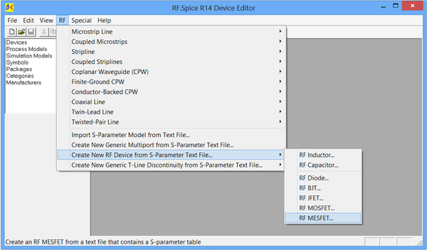
Create two text files as indicated in the tables above. Open [[RF.Spice]]'s Device Editor and select "Create New RF Device from S-Parameter Test File..." from its RF Menu. Follow the program's prompts step by step and create your new RF BJT and MESFET devices. | Create two text files as indicated in the tables above. Open [[RF.Spice]]'s Device Editor and select "Create New RF Device from S-Parameter Test File..." from its RF Menu. Follow the program's prompts step by step and create your new RF BJT and MESFET devices. | ||
| − | |||
| − | |||
| − | |||
| − | |||
| − | |||
| − | |||
| − | |||
| − | |||
| − | |||
| − | |||
| − | |||
| − | |||
| − | |||
| − | |||
| − | |||
| − | |||
| − | |||
| − | |||
| − | |||
| − | |||
| − | |||
| − | |||
| − | |||
| − | |||
| − | |||
| − | |||
| − | |||
| − | |||
| − | |||
| − | |||
| − | |||
| − | |||
| − | |||
| − | |||
| − | |||
| − | |||
| − | |||
| − | |||
| − | |||
| − | |||
| − | |||
| − | |||
| − | |||
| − | |||
| − | |||
| − | |||
| − | |||
| − | |||
| − | |||
| − | |||
| − | |||
| − | |||
| − | |||
| − | |||
| − | |||
| − | |||
| − | |||
| − | |||
| − | |||
| − | |||
| − | |||
| − | |||
| − | |||
| − | |||
| − | |||
| − | |||
| − | |||
| − | |||
| − | |||
| − | |||
| − | |||
| − | |||
| − | |||
| − | |||
| − | |||
| − | |||
| − | |||
| − | |||
| − | |||
| − | |||
| − | |||
| − | |||
| − | |||
| − | |||
| − | |||
| − | |||
| − | |||
| − | |||
| − | |||
| − | |||
| − | |||
| − | |||
| − | |||
| − | |||
| − | |||
| − | |||
| − | |||
| − | |||
| − | |||
| − | |||
| − | |||
| − | |||
| − | |||
| − | |||
| − | |||
| − | |||
| − | |||
| − | |||
| − | |||
| − | |||
| − | |||
| − | |||
| − | |||
| − | |||
| − | |||
| − | |||
| − | |||
| − | |||
| − | |||
| − | |||
| − | |||
| − | |||
| − | |||
| − | |||
| − | |||
| − | |||
| − | |||
| − | |||
| − | |||
| − | |||
| − | |||
| − | |||
| − | |||
| − | |||
| − | |||
| − | |||
| − | |||
| − | |||
| − | |||
| − | |||
| − | |||
| − | |||
| − | |||
| − | |||
| − | |||
| − | |||
| − | |||
| − | |||
| − | |||
| − | |||
| − | |||
| − | |||
| − | |||
| − | |||
== Building a Distributed MESFET Amplifier with Microstrip Components== | == Building a Distributed MESFET Amplifier with Microstrip Components== | ||
Revision as of 14:11, 5 September 2015
Analyzing Distributed RF Amplifiers With Imported BJT & FET Models
Objective
In the first part of this tutorial, you will learn how to import RF BJT and FET models from text files. In the second part, you will build a distributed RF amplifier using a bilateral RF BJT and generic transmission line components. In the third part, you will build a distributed RF amplifier from an imported unilateral MESFET using physical microstrip components for the input and output matching networks.
Importing High Frequency Transistor Models
RF.Spice's Parts Database contains a sizable collection of RF diodes and BJTs. As you saw in the previous tutorial lesson, each S-Parameter BJT model corresponds to a certain DC operating point. Therefore, you will find a large number of RF BJT models associated with the same device but measured at different values of VCE and IC. The manufacturer data sheets of RF transistors usually contains a table of measured S-parameter data in the following format:
# GHz s ma r 50
freq1 |s11| ∠s11 |s21| ∠s21 |s12| ∠s12 |s22| ∠s22
freq2 |s11| ∠s11 |s21| ∠s21 |s12| ∠s12 |s22| ∠s22
freq3 |s11| ∠s11 |s21| ∠s21 |s12| ∠s12 |s22| ∠s22
...
You can import text files with a ".TXT" file extension containing S-parameter data of the above format to RF.Spice. Better yet, you can create new active RF devices and add them to expand your Parts Database. To create a new device, you need to add the following to lines to the header of your text file:
.model <model_name>
.symbol <symbol_name>
The first line creates a unique model names in the database and the second line picks the right symbol, which is usually either "npn_bjt_2port", or "jfet_n" or "mosfet_n" or "mesfet_n", or their p-type counterparts. For this tutorial lesson, you need to create an RF BJT and an RF MESFET.
The measured data for the RF BJT device are given below:
| File Name | Model Name | Symbol Name | Symbol |
|---|---|---|---|
| MyRFBJT.txt | MyRFBJT | bjt_npn_2port | 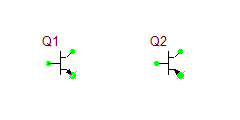
|
| f(GHz) | s11 | s21 | s12 | s22 |
|---|---|---|---|---|
| 3.0 | 0.80 ∠ -89 ° | 2.86 ∠ 99 ° | 0.03 ∠ 56 ° | 0.76 ∠ -41 ° |
| 4.0 | 0.72 ∠ -116 ° | 2.60 ∠ 76 ° | 0.03 ∠ 57 ° | 0.73 ∠ -54 ° |
| 5.0 | 0.66 ∠ -142 ° | 2.39 ∠ 54 ° | 0.03 ∠ 62 ° | 0.72 ∠ -68 ° |
Your MyRFBJT.txt file should look like the following:
.model MyRFBJT
.symbol bjt_npn_2port
3.0 0.80 -89 2.86 99 0.03 56 0.76 -41
4.0 0.72 -116 2.60 76 0.03 57 0.73 -54
5.0 0.66 -142 2.39 54 0.03 62 0.72 -68
The measured data for the MESFET device are given below:
| File Name | Model Name | Symbol Name | Symbol |
|---|---|---|---|
| MyMESFET.txt | MyMESFET | mesfet_n | 
|
| f(GHz) | s11 | s21 | s12 | s22 |
|---|---|---|---|---|
| 3.0 | 0.80 ∠ -90 ° | 2.80 ∠ 100 ° | 0 | 0.66 ∠ -50 ° |
| 4.0 | 0.75 ∠ -120 ° | 2.50 ∠ 80 ° | 0 | 0.60 ∠ -70 ° |
| 5.0 | 0.71 ∠ -140 ° | 2.30 ∠ 60 ° | 0 | 0.58 ∠ -85 ° |
Create two text files as indicated in the tables above. Open RF.Spice's Device Editor and select "Create New RF Device from S-Parameter Test File..." from its RF Menu. Follow the program's prompts step by step and create your new RF BJT and MESFET devices.
Building a Distributed MESFET Amplifier with Microstrip Components
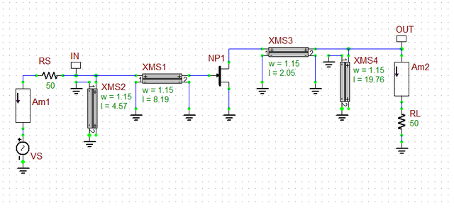
The following is a list of parts needed for this part of the tutorial lesson:
AC Voltage Source: VS (keyboard shortcut: Alt+V)
Two 50Ω Resistors: RS and RL
N-Type MESFET: MyMESFET (imported model)
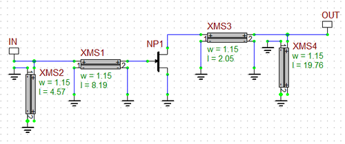
Four Microtrip Line Segments: XMS1, XMS2, XMS3 and XMS4 (keyboard shortcut: Alt+T)
Two Ammeters: AM1 and AM2 (keyboard shortcut: Alt+Y)
Two Net Markers: IN and OUT (keyboard shortcut: Alt+N)
The goal of this part is to design a distributed MESFET amplifier with a gain of 11dB at f = 4GHz. From the S-parameter data of the MESFET, we know that it is a unilateral transistor, i.e. s12 = 0. Moreover, |s11| < 1 and |s22| < 1. Therefore, the MESFET is unconditionally stable. This reduces the input and output reflection coefficients to:
[math] \Gamma_{in} = s_{11} [/math]
[math] \Gamma_{out} = s_{22} [/math]
The conjugate matching conditions at the input and output of the unilateral transistor reduce to:
[math] \Gamma_S = s_{11}^{\ast} [/math]
[math] \Gamma_L = s_{22}^{\ast} [/math]
Furthermore, you have:
[math] G_0 = |s_{21}|^2 = 6.25 = 8.0dB [/math]
[math] G_{Tmax} = G_S . G_0 . G_L = \frac{1}{1- |s_{11}| ^2} . |S_{21}|^2 . \frac{1}{1- |s_{22}| ^2} = 13.5dB [/math]
To achieve a gain of 11dB, you have 2.5dB more available gain. So you set GS = 2dB and GL = 1dB for a total gain of GT = 2dB + 8dB + 1dB = 11dB. The complex value of ΓS is found on the constant circle GS = 2dB, and the complex value of ΓL is found on the constant circle GL = 1dB, in both cases trying to minimize the distance from the center of the Smith Chart. This requirement yields:
ΓS = 0.33 ∠120°
ΓL = 0.22 ∠70°
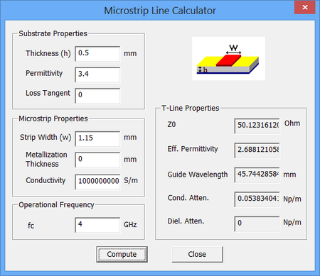
For your MESFET amplifier, you will use the same input and output matching network types of the previous part consisting of a 50Ω transmission line segment together with a shunt 50Ω Open Stub. For this project, you will use a thin lossless dielectric substrate of thickness h = 0.5mm and relative permittivity &epsilonr = 3.4. A 50Ω microstrip line on this substrate has a width of 1.15mm. At the design frequency of f = 4GHz, the guide wavelength of this microstrip line is λg = 45.74mm.
The lengths of the microstrip segments are found to be:
| Microstrip Component | Z0 | Electrical Length | Physical Width | Physical Length |
|---|---|---|---|---|
| XMS1 | 50Ω | 0.179λg | 1.15mm | 8.19mm |
| XMS2 | 50Ω | 0.100λg | 1.15mm | 4.57mm |
| XMS3 | 50Ω | 0.045λg | 1.15mm | 2.05mm |
| XMS4 | 50Ω | 0.432λg | 1.15mm | 19.76mm |
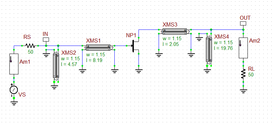
Place and connect all the parts as shown in the above figure. For the shunt stubs, connect the microstrip segments XMS2 and XMS4 in a parallel fashion between the source and load resistors and the ground, respectively. First, remove the AC voltage source and the source and load resistors to perform network analysis. Run a Network Analysis Test of this circuit with start and stop frequencies set at 3GHz and 5GHz, respectively, with a linear frequency step size of 10MHz. Plot the S-parameters on an amplitude-only Cartesian graph. The figure below shows the results for s11, s21, s12 and s22 parameters. Note that since s12 = 0, its dB-scale plot falls at a very large negative number. Therefore, you need to adjust the scale of the vertical axis. The insertion gain |s21| is almost 11dB as expected from the design. However, the value of the return loss |s11| is only -5dB and certainly not very good. This is due to the fact that you had to deliberately introduce a mismatch in the input and output matching networks to achieve the specified gain of 11dB.
Next, connect the AC voltage source and the source and load resistors and place the source and load ammeters in a similar manner as in the last part of this tutorial lesson. Similarly, define a custom output plot called GP for the power gain of your amplifier. Use the same definition: GP = 20*log10(abs(i(am2)/i(am1))). Run an AC Frequency Sweep Test of your amplifier from 3GHz to 5GHz with linear frequency steps of 10MHz. The figure below shows the graph of power gain vs. frequency.
