|
|
| (One intermediate revision by the same user not shown) |
| Line 14: |
Line 14: |
| | | | |
| | In this tutorial lesson, you will first build and analyze binary half adder and full adder circuits made up of logic gates. Then you will create a new database part out of the full adder circuit. Finally, you will use the new full adder part to build a four-bit ripple-carry adder digital circuit. | | In this tutorial lesson, you will first build and analyze binary half adder and full adder circuits made up of logic gates. Then you will create a new database part out of the full adder circuit. Finally, you will use the new full adder part to build a four-bit ripple-carry adder digital circuit. |
| − |
| |
| − | === Building a Binary Half Adder ===
| |
| − |
| |
| − | [[File:TUT9-1.png|thumb|350px|The Binary Half Adder digital circuit.]]
| |
| − | The following is a list of parts needed for this part of the tutorial lesson:
| |
| − |
| |
| − | ----
| |
| − |
| |
| − | Digital Input: A (keyboard shortcut: N)
| |
| − |
| |
| − | Digital Input: B (keyboard shortcut: N)
| |
| − |
| |
| − | XOR Gate (keyboard shortcut: X)
| |
| − |
| |
| − | AND Gate (keyboard shortcut: A)
| |
| − |
| |
| − | Digital Output: S (keyboard shortcut: O)
| |
| − |
| |
| − | Digital Output: C (keyboard shortcut: O)
| |
| − |
| |
| − | ----
| |
| − |
| |
| − | The binary half adder is a digital circuit that adds two single binary bits A and B. It has two outputs, sum (S) and carry (C). The carry signal represents an overflow into the next significant bit of a multi-bit addition. The equivalent decimal value of the binary sum is 2C + S. The half adder can be built using an XOR gate and an AND gate as shown in the opposite figure.
| |
| − |
| |
| − | Connect the parts as shown in the figure. Run a live [[Digital Simulation|digital simulation]]. When simulating digital circuit, instead of "Run", you use the "Step" feature. At every time step, that state of all the digital outputs are updated based on the latest states of the digital inputs. Click the "'''Step'''" [[File:b2Step_Tool.png]] button of the '''[[Toolbars#Main_Toolbar |Main Toolbar]]''' or simply use the keyboard shortcut "'''Ctrl+H'''". To generate the truth table of the half adder, set the values of the inputs A and B using their up and down arrow buttons to (0,0), (1,0), (0,1) and (1,1) at each time step, consecutively. Note that when you change the input values, the output does not change instantaneously until your increment the time step. The truth table of the binary half adder and two simulation scenarios are shown in the figures below. In a live [[Digital Simulation|digital simulation]], B2.Spice's Circuit [[Animation]] feature is always enabled by default. You can see the binary of all the wire. Also note how all the wires of the circuit are color-coded in red and blue for 1 (High) and 0 (Low) states, respectively.
| |
| − |
| |
| − |
| |
| − | {| class="wikitable" style="text-align:center"
| |
| − | |-
| |
| − | !colspan="2"| Inputs !!colspan="2"| Outputs
| |
| − | |-
| |
| − | ! ''A'' !! ''B'' !! ''C'' !! ''S''
| |
| − | |-
| |
| − | | 0 || 0 || 0 || 0
| |
| − | |-
| |
| − | | 1 || 0 || 0 || 1
| |
| − | |-
| |
| − | | 0 || 1 || 0 || 1
| |
| − | |-
| |
| − | | 1 || 1 || 1 || 0
| |
| − | |-
| |
| − | |}
| |
| − |
| |
| − |
| |
| − | <table>
| |
| − | <tr>
| |
| − | <td>
| |
| − | [[File:TUT9-2.png|thumb|350px|The outputs of the Binary Half Adder when A = 1 and B = 0.]]
| |
| − | </td>
| |
| − | <td>
| |
| − | [[File:TUT9-3.png|thumb|350px|The outputs of the Binary Half Adder when A = B = 1.]]
| |
| − | </td>
| |
| − | </tr>
| |
| − | </table>
| |
| − |
| |
| − |
| |
| − | === Creating a Digital Device from Your Adder Circuit ===
| |
| − |
| |
| − | [[File:TUT9-9.png|thumb|450px|The property dialogs of Digital Input and Digital Output parts.]]
| |
| − | Before you proceed to the next part of this tutorial, you will create a reusable digital part out of your binary half added circuit. This procedure is very similar but much simpler than the case of analog circuits you carried out in Tutorial Lesson 6. If you open the property dialog of your digital inputs or outputs, you will notice that a checkbox labeled "Use As Subcircuit Port" has been already been checked by default. This means that [[B2.Spice A/D]] takes your digital circuit with all the designated input and output ports and packages it as a digital device "As Is".
| |
| − |
| |
| − |
| |
| − | Go the File Menu and select "Create Part from Circuit..." or simply use the keyboard shortcut "Ctrl+M". A dialog pops up asking you to enter a name for your new device. Enter "MyHA" (My Half Adder) for the name. Then, the program asks you if you want it to create a symbol for your new device. Answer yes and proceed. The device will be generated and added to your Parts Database. Keep in mind that you can create your own symbols or modify the program-generated symbol using B2.SPice's Symbol Editor.
| |
| − |
| |
| − |
| |
| − | === Building a Binary Full Adder ===
| |
| − |
| |
| − | [[File:TUT9-4.png|thumb|420px|The Binary Full Adder digital circuit.]]
| |
| − | The following is a list of parts needed for this part of the tutorial lesson:
| |
| − |
| |
| − | ----
| |
| − |
| |
| − | Digital Input: A (keyboard shortcut: N)
| |
| − |
| |
| − | Digital Input: B (keyboard shortcut: N)
| |
| − |
| |
| − | Digital Input: Cin (keyboard shortcut: N)
| |
| − |
| |
| − | Two XOR Gates (keyboard shortcut: X)
| |
| − |
| |
| − | Two AND Gates (keyboard shortcut: A)
| |
| − |
| |
| − | OR Gate (keyboard shortcut: U)
| |
| − |
| |
| − | Digital Output: S (keyboard shortcut: O)
| |
| − |
| |
| − | Digital Output: Cout (keyboard shortcut: O)
| |
| − |
| |
| − | ----
| |
| − |
| |
| − |
| |
| − | A binary full adder is a digital circuit that adds two single binary bits A and B and accounts for values carried in as well as out. It adds three bits: A, B, and Cin, a bit carried in from the previous less significant stage. The circuit produces a two-bit output, sum (S) and output carry (C). The equivalent decimal value of the binary sum is 2Cout + S.
| |
| − |
| |
| − | A full adder can be constructed from two half adders by feeding the inputs A and B to the first half adder, connecting the sum from the first half adder to an input to the second half adder, connecting Cin to the other input of the second half adder and passing the two carry outputs of the two half adders through an OR gate.
| |
| − |
| |
| − | Connect the parts as shown in the opposite figure. Run a live [[Digital Simulation|digital simulation]] of your circuit using manual stepping. Generate the truth table of the full adder circuit in a similar manner as in the previous case. However, in this case, first you set Cin = 0, change the values of A and B, and then you set Cin = 1, and repeat the procedure. The truth table of the binary full adder and four different simulation scenarios are shown in the figures below. As you can see from the figures, B2.Spice's color coding of the digital wires comes in very handy.
| |
| − |
| |
| − |
| |
| − | {| class="wikitable" style="text-align:center"
| |
| − | |-
| |
| − | !colspan="3"| Inputs !!colspan="2"| Outputs
| |
| − | |-
| |
| − | ! ''A'' !! ''B'' !! ''C''<sub>in</sub> !! ''C''<sub>out</sub> !! ''S''
| |
| − | |-
| |
| − | | 0 || 0 || 0 || 0 || 0
| |
| − | |-
| |
| − | | 1 || 0 || 0 || 0 || 1
| |
| − | |-
| |
| − | | 0 || 1 || 0 || 0 || 1
| |
| − | |-
| |
| − | | 1 || 1 || 0 || 1 || 0
| |
| − | |-
| |
| − | | 0 || 0 || 1 || 0 || 1
| |
| − | |-
| |
| − | | 1 || 0 || 1 || 1 || 0
| |
| − | |-
| |
| − | | 0 || 1 || 1 || 1 || 0
| |
| − | |-
| |
| − | | 1 || 1 || 1 || 1 || 1
| |
| − | |}
| |
| − |
| |
| − |
| |
| − | <table>
| |
| − | <tr>
| |
| − | <td>
| |
| − | [[File:TUT9-5.png|thumb|420px|The outputs of the Binary Full Adder when Cin = 0 and A = B = 1.]]
| |
| − | </td>
| |
| − | <td>
| |
| − | [[File:TUT9-6.png|thumb|420px|The outputs of the Binary Full Adder when Cin = 1 and A = B = 0.]]
| |
| − | </td>
| |
| − | </tr>
| |
| − | <tr>
| |
| − | <td>
| |
| − | [[File:TUT9-7.png|thumb|420px|The outputs of the Binary Full Adder when Cin = 1 and A = 1 and B = 0.]]
| |
| − | </td>
| |
| − | <td>
| |
| − | [[File:TUT9-8.png|thumb|420px|The outputs of the Binary Full Adder when Cin = 1 and A = B = 1.]]
| |
| − | </td>
| |
| − | </tr>
| |
| − | </table>
| |
| − |
| |
| − |
| |
| − | Before you proceed to the next of this tutorial lesson, create a new part from your binary full adder circuit. Follow the same procedure as in the previous case and choose the name "MyFA" (My Full Adder) for your new device.
| |
| − |
| |
| | | | |
| | === Building a Ripple-Carry Adder === | | === Building a Ripple-Carry Adder === |
| Line 199: |
Line 55: |
| | | | |
| | <p> </p> | | <p> </p> |
| − | [[Image:Back_icon.png|40px]] '''[[RF.Spice_A/D | Back to RF.Spice A/D Wiki Gateway]]''' | + | [[Image:Back_icon.png|40px]] '''[[RF.Spice_A/D#RF.Spice_A.2FD_Tutorial | Back to RF.Spice A/D Tutorial Gateway]]''' |
In this tutorial lesson, you will first build and analyze binary half adder and full adder circuits made up of logic gates. Then you will create a new database part out of the full adder circuit. Finally, you will use the new full adder part to build a four-bit ripple-carry adder digital circuit.
You can use multiple full adders to build an N-bit adder circuit. Each full adder inputs a Cin, which is the Cout of the previous adder. This kind of adder is called a ripple-carry adder, since each carry bit "ripples" to the next full adder. Note that the first (and only the first) full adder may be replaced by a half adder (under the assumption that Cin = 0).
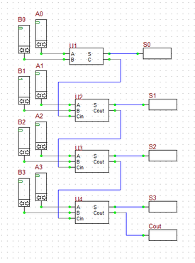
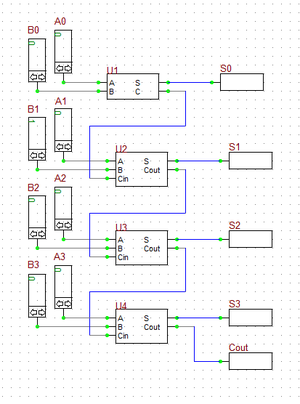
In the last part of this tutorial lesson, you will build a 4-bit ripple-carry binary adder using the half adder and full adder devices you create in the previous parts. Open a new blank project, place all the parted listed above and connect then as shown in the figure. To place your new adder parts, you can either go to the Parts Bin of the Toolbox and search for "MyHA" and "MyFA" alphabetically under the letter "M", or you can open the "Select Device Dialog" by choosing "Select Part..." from the Parts Menu. Note that the half adder block U1 is used for the least significant bits A0 and B0, and the full adder block U2, U3 and U4 are used for the more significant bits. The "Cout" output of the last full adder block U4 summing the most significant bits A4 and B2 is taken out as the "Carry" output of the whole circuit.
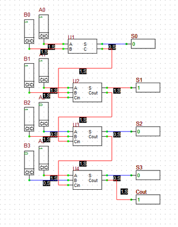
You can run different simulation scenarios by inputting 4-bit binary numbers to A's and B's. The figures below show two of such scenarios. In the figure on the left, A = 1001 (9) and B = 0011 (3). The sum is 1100 representing the decimal number 12. In the figure on the right, A = 1011 (11) and B = 0111 (7). The sum of these inputs must be the decimal number 18, which is equivalent to 0010 with a carry of 1 in a 4-bit system (i.e. 2 + 16), which can be seen in the figure.


