Digital Tutorial Lesson 5: Creating Reusable Digital Devices - Binary Half & Full Adders
Contents
What You Will Learn
In this tutorial you will first build and analyze binary half adder and full adder circuits made up of logic gates. Then, you will create a new reusable digital device out of the full adder circuit and will store it in the RF.Spice A/D parts database for later use.
Building a Binary Half Adder
The following is a list of parts needed for this part of the tutorial lesson:
| Part Name | Part Type | Part Value |
|---|---|---|
| A | Digital Input | 1-bit |
| B | Digital Input | 1-bit |
| Out1 | Digital Output | N/A |
| S | Digital Output | N/A |
| C | Digital Output | N/A |
| A1 | Generic XOR Gate | Defaults |
| A2 | Generic AND Gate | Defaults |
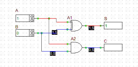
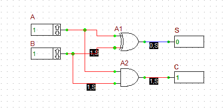
The binary half adder is a digital circuit that adds two single binary bits A and B. It has two outputs, sum (S) and carry (C). The carry signal represents an overflow into the next significant bit of a multi-bit addition. The equivalent decimal value of the binary sum is 2C + S. The half adder can be built using an XOR gate and an AND gate as shown in the figure below.
Connect the parts as shown in the figure. Run a live digital simulation by stepping in time. Use the same time step of 20ns as in the previous tutorial lessons. To generate the truth table of the half adder, set the values of the inputs A and B using their up and down arrow buttons to (0,0), (1,0), (0,1) and (1,1) at each time step, consecutively. Note that when you change the input values, the output does not change instantaneously until your increment the time step. The truth table of the binary half adder and two simulation scenarios are shown in the figures below. In a live digital simulation, RF.Spice's Circuit Animation feature is always enabled by default. You can see the binary state of all the wires. Also note how all the wires of the circuit are color-coded in red and blue for 1 (High) and 0 (Low) states, respectively.
| Inputs | Outputs | ||
|---|---|---|---|
| A | B | C | S |
| 0 | 0 | 0 | 0 |
| 1 | 0 | 0 | 1 |
| 0 | 1 | 0 | 1 |
| 1 | 1 | 1 | 0 |
Creating a Reusable Digital Device from Your Half Adder Circuit
In this part of the tutorial lesson, you will create a reusable digital device out of your binary half adder circuit. This procedure is very similar but much simpler than the case of analog circuits you carried out in Analog Tutorial Lesson 5. If you open the property dialog of your digital inputs or outputs, you will notice that a checkbox labeled Use As Subcircuit Port has been already been checked by default. This means that RF.Spice A/D takes your digital circuit with all the designated input and output ports and packages it as a digital device "As Is".
Go the File Menu and select Create Part from Circuit… or simply use the keyboard shortcut Ctrl+M}. A dialog pops up asking you to enter a name for your new device. Enter "MyHA" (My Half Adder) for the name of your half adder circuit. Then, the program asks you if you want it to create a symbol for your new device. Answer "Yes" and proceed. The device will be generated and added to your Parts Database. Keep in mind that you can create your own symbols or modify the program-generated symbol using RF.Spice's Symbol Editor.
Building a Binary Full Adder
The following is a list of parts needed for this part of the tutorial lesson:
| Part Name | Part Type | Part Value |
|---|---|---|
| A | Digital Input | 1-bit |
| B | Digital Input | 1-bit |
| Cin | Digital Input | 1-bit |
| Out1 | Digital Output | N/A |
| S | Digital Output | N/A |
| Cout | Digital Output | N/A |
| A1 | Generic XOR Gate | Defaults |
| A2 | Generic AND Gate | Defaults |
| A3 | Generic XOR Gate | Defaults |
| A4 | Generic AND Gate | Defaults |
| A5 | Generic OR Gate | Defaults |
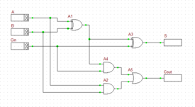
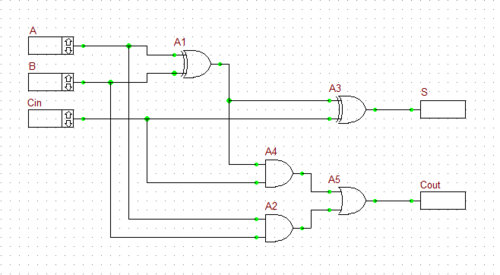
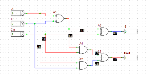
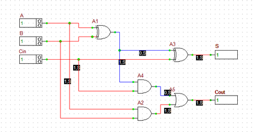
A binary full adder is a digital circuit that adds two single binary bits A and B and accounts for values carried in as well as out. It adds three bits: A, B, and Cin, a bit carried in from the previous less significant stage. The circuit produces a two-bit output, sum (S) and output carry (C). The equivalent decimal value of the binary sum is 2Cout + S. A full adder can be constructed from two half adders by feeding the inputs A and B to the first half adder, connecting the sum from the first half adder to an input to the second half adder, connecting Cin to the other input of the second half adder and passing the two carry outputs of the two half adders through an OR gate.
Connect the parts as shown in the opposite figure.
Run a live digital simulation of your circuit using manual stepping. Generate the truth table of the full adder circuit in a similar manner as in the previous case. However, in this case, first you set Cin = 0, change the values of A and B, and then you set Cin = 1, and repeat the procedure. The truth table of the binary full adder and four different simulation scenarios are shown in the figures below. As you can see from the figures, RF.Spice's color coding of the digital wires comes in very handy.
| Inputs | Outputs | |||
|---|---|---|---|---|
| A | B | Cin | Cout | S |
| 0 | 0 | 0 | 0 | 0 |
| 1 | 0 | 0 | 0 | 1 |
| 0 | 1 | 0 | 0 | 1 |
| 1 | 1 | 0 | 1 | 0 |
| 0 | 0 | 1 | 0 | 1 |
| 1 | 0 | 1 | 1 | 0 |
| 0 | 1 | 1 | 1 | 0 |
| 1 | 1 | 1 | 1 | 1 |
Creating a Reusable Digital Device from Your Full Adder Circuit
Using the same procedure you carried out earlier in this tutorial lesson, create a new reusable digital device out of your full adder circuit. Choose the name "MyFA" (My Full Adder) for your new device and let RF.Spice A/D create a default automatic symbol for the device. Note that "MyHA" was a 4-pin device with 2 input pins and 2 output pins, while "MyFA" is a 5-pin device with 3 input pins and 2 output pins. You will use both of your new reusable digital devices for the construction of the circuit of the next tutorial lesson.
