Digital Tutorial Lesson 3: Building a Shift Register Using D Flip-Flops
Exploring Flip-Flops and Sequential Logic Circuits
Contents
Objective
In this tutorial lesson, first you will build SR flip-flop circuits out of logic gates. You will examine their truth table and use them to verify the operation of B2.Spice's own generic SR latch device. Then you will examine B2.Spice's D flip-flop device and will use four D flip-flops to design a 4-bit shift register. Finally, you will examine B2.Spice's JK flip-flop device and will use four JK flip-flops to design a 4-bit binary counter. You will use both the live timing diagrams and transient analysis in this tutorial lesson.
Building and Testing an SR Latch
The following is a list of parts needed for this part of the tutorial lesson:
Digital Input: S (keyboard shortcut: N)
Digital Input: S (keyboard shortcut: N)
Digital Input: EN (keyboard shortcut: N)
Two NOR Gates (keyboard shortcut: Alt+U)
Two AND Gates (keyboard shortcut: A)
Digital Output: Q (keyboard shortcut: O)
Digital Output: Q_bar (keyboard shortcut: O)
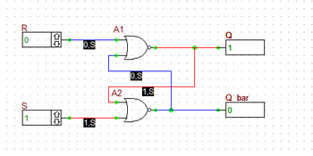
First, build the basic SR latch using two cross-coupled NOR gates as shown in the above figure. Before starting the simulation, manually set the inputs as S = 1 and R = 0. This is the "SET" state of the latch. Run a live digital simulation by manual stepping. Click the "Step" ![]() button of the Main Toolbar or simply use the keyboard shortcut "Ctrl+H". Note that the Q output changes to 1, while its complement Q_bar changes to 0. Change S to 0. Now, you have S = R = 0. This is the "HOLD" state. Step the simulation, and you will note that the output do not change at this state. Now change R to 1, while S is still at 0. This is the "RESET" state of the latch. Step the simulation and you will see that Q changes to 0 and Q_bar turns 1.
button of the Main Toolbar or simply use the keyboard shortcut "Ctrl+H". Note that the Q output changes to 1, while its complement Q_bar changes to 0. Change S to 0. Now, you have S = R = 0. This is the "HOLD" state. Step the simulation, and you will note that the output do not change at this state. Now change R to 1, while S is still at 0. This is the "RESET" state of the latch. Step the simulation and you will see that Q changes to 0 and Q_bar turns 1.
The truth table of the basic NOR SR latch is given below:
|
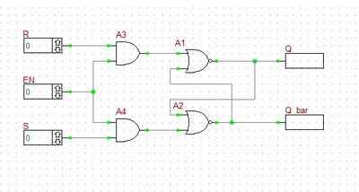
Next, you will add an "Enable" input to your SR latch using two AND gates as shown in the opposite figure. The EN input is fed into both AND gates. Therefore, as long as EN =0, the output of both AND gates is 0. This leads to S = R = 0, which represents the Hold state of the basic NOR SR latch. Before you start the simulation, set EN = 0. Then, set S = 1 and R = 0. Start a live digital simulation by manual stepping. Unlike the previous case, the output Q and Q_bar do not change this time. Next, set EN = 1. step the simulation and you will see that outputs change to Q = 1 and Q_bar = 0 (Set state). While EN = 1, change to S = 0 and R = 1. Step through and the gated latch enters its Reset sate with Q = 0 and Q_bar = 1.
The truth table of the gated NOR SR latch is given below:
|
Verifying B2.Spice's SR Latch Device
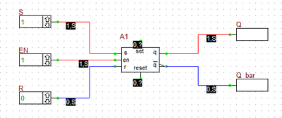
Next, you will remove the two NOR and two AND gates from you digital circuit and replace the four gates with an SR latch device. Connect the input S and R pins and output Q and Q_bar outputs pins of the device as shown in the figure below. Note that unlike the previous circuit, here the top and bottom inputs are called S and R, respectively. Repeat the same procedure in the last part and change the values of the three inputs S, R, and EN in the same manner. You should be able to reproduce the above truth table for this circuit, too.
Testing a D Flip-Flop
The following is a list of parts needed for this part of the tutorial lesson:
Digital Input: In1 (keyboard shortcut: N)
Digital Clock: CLK (keyboard shortcut: Alt+C)
D-Type Flip-Flop
Digital Output: Out1 (keyboard shortcut: O)
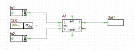
This part of the tutorial lesson is very similar to the last part, except for replacing the SR latch with the D flip-flop. You will build a synchronous circuit with a digital clock and a single input as shown in the opposite figure. Set the "Period" of the clock to 100ns and its "Pulse Width" to 50ns. Connect the digital input device to the "D" pin of the flip-flop and the digital output device to its "Q" pin. The D flip-flop transfers the input data at its input to its Q output on the rising edge of the clock pulse. During the rest of the clock cycle, the output remains unchanged (hold state).
To understand the operation of the flip-flop circuit, you will use the "Live Digital Timing Diagram" feature of B2.Spice A/D. First, click the button labeled "..." on the Main Toolbar on the left of the Run button or use the keyboard shortcut "Ctrl+I" to open the "Simulation Time Options" dialog. Set the step time to 20ns. Set the input initially to In1 = 0. Then, to activate the timing diagram, click the "Show/Hide Live Digital Timing Diagrams" ![]() button of the Schematic Toolbar. Remember that nothing will happen until you start a digital simulation. Click the "Step"
button of the Schematic Toolbar. Remember that nothing will happen until you start a digital simulation. Click the "Step" ![]() button of the Main Toolbar or use the keyboard shortcut "Ctrl+H" to advance the simulation time one step at a time. Step the simulation time to 60ns and then change the input to In1 = 1. Keep stepping to 160ns and then change the input to In1 = 0 again. Continue stepping to 400ns and change the input to In1 = 1 once again and then proceed to 600ns. The table below summarizes the input entries:
button of the Main Toolbar or use the keyboard shortcut "Ctrl+H" to advance the simulation time one step at a time. Step the simulation time to 60ns and then change the input to In1 = 1. Keep stepping to 160ns and then change the input to In1 = 0 again. Continue stepping to 400ns and change the input to In1 = 1 once again and then proceed to 600ns. The table below summarizes the input entries:
| |
The timing diagram updates only when there is a change of states of the inputs. |
| Time | In1 |
|---|---|
| 0ns | 0 |
| 160ns | 1 |
| 260ns | 0 |
| 400ns | 1 |
The timing diagram of your D flip-flop circuit is shown in the above figure. As you can see from the figure, the input first rises from 0 to 1 at t = 160ns. The flip-flop waits until the next rising edge of the clock signal at t = 200ns. The input's high state is transferred to the output Q with a propagation delay of 14ns. According to the property dialog of the D Flip-Flop device, the low-to-high propagation delay of the device is tPLH = 14ns, while its high-to-low propagation delay is tPHL = 1420ns. Therefore, Q rises from 0 to 1 at t = 214ns and stays high for the next several clock cycles. The input next falls from 1 to 0 at t = 260ns. The flip-flop waits until the next rising edge of the clock signal at t = 300ns. The input's low state is transferred to the output Q with a propagation delay of 20ns. Therefore, Q falls from 1 to 0 at t = 320ns and stays low for the next several clock cycles. The input rises again from 0 to 1 at t = 400ns and stay high for the rest of the simulation time. This time the flip-flop has to wait a full clock period until the next rising edge of the clock signal at t = 500ns. The input's high state is transferred to the output Q with a propagation delay of 14ns. Then, Q rises again from 0 to 1 at t = 514ns and stays high for the rest of the simulation time.
B2.Spice's digital timing diagrams are live graphs that evolve in real time. When you step the simulation for too long, the diagram exceeds the extents of your screen, and a horizontal scroll bar soon appears at the bottom of the diagram. To see the whole diagram without scrolling, you can zoom out its view horizontally. Click on the tab of the diagram at the bottom window to make its view active. The Graph Toolbar appears and replaces the Schematic Toolbar. Click the "Zoom Out Horizontally" ![]() button of the Graph Toolbar to squeeze the timing diagram horizontally to the point it fits in the screen.
button of the Graph Toolbar to squeeze the timing diagram horizontally to the point it fits in the screen.
Building a 4-Bit Shift Register Using D Flip-Flops
The following is a list of parts needed for this part of the tutorial lesson:
Digital Input: Data (keyboard shortcut: N)
Digital Clock: CLK (keyboard shortcut: Alt+C)
Four D-Type Flip-Flops
Four Digital Output: B0, B1, B3 and B4 (keyboard shortcut: O)
A shift register is a multi-output digital circuit that transfer the input data to its outputs sequentially at each clock cycle. Cascade the four D flip-flops as shown on the figure by connecting the Q pin of each to the D pin of the next. All four flip-flops share the same clock signal. Use the same clock settings from the previous part (Period = 100ns and Pulse Width = 50ns). Set the step time to 20ns. Enable the live digital timing diagram. Run a digital simulation and step through 1200ns. Set the value of the input "Data" to 0 and change it to 1 at t = 100ns and change it back to 0 at t = 600ns.
Your timing diagram will look like the figure below. As you can see from the figure, after the input is set high at t = 100ns for the first time, it takes the first flip-flop until the clock's next rising edge at t = 200ns to react. The first output B0 rises to 1 at t = 214ns (tPLH = 14ns). As the clock cycles proceed, the other outputs B1, B2 and B3, sequentially rise to 1 at t = 314ns, 414ns, and 514ns, respectively. All four outputs remain high for the next several clock cycles (at hold state).
The input "Data" next falls from 1 to 0 at t = 600ns. It takes the first flip-flop until the clock's next rising edge at t = 700ns to react. The first output B0 fall from to 0 at t = 720ns (tPHL = 20ns). As the clock cycles proceed, the other outputs B1, B2 and B3, sequentially fall to 0 at t = 820ns, 902ns, and 1020ns, respectively. All four outputs remain low afterwards (at hold state).
Testing a JK Flip-Flop
The following is a list of parts needed for this part of the tutorial lesson:
Digital Input: In1 (keyboard shortcut: N)
Digital Input: In2 (keyboard shortcut: N)
Digital Clock: CLK (keyboard shortcut: Alt+C)
JK-Type Flip-Flop
Digital Output: Out1 (keyboard shortcut: O)
Digital Output: Out2 (keyboard shortcut: O)
The JK Flip-Flop acts like a sequential (clocked) SR latch with its J and K inputs used for "Set" and "Reset" functions. The case of J = K = 0 represents the "Hold State". By contrast, the case of J = K = 1 is not illegal, but representing the "Toggle State". All the changes occur at the rising edge of the clock signal. Connect the JK Flip-Flop to the input and output devices as shown in the opposite figure.
Set the time step to 20ns. Set both input values to zero initially. Run a live digital simulation and observe the timing diagram of the circuit. Step the simulation sequentially until t = 1200ns. Change the input values according to the table below:
| Time | In1 | In2 |
|---|---|---|
| 0ns | 0 | 0 |
| 60ns | 1 | 0 |
| 160ns | 0 | 1 |
| 360ns | 1 | 1 |
| 640ns | 0 | 0 |
| 800ns | 0 | 1 |
The timing diagram is shown in the figure below. Note that the propagation delay times of the JK Flip-Flop device are tPLH = 16ns and tpHL = 25ns. The flip-flop is "set" at t = 60ns (J = 1 and K = 0). It takes until the clock's rising edge at t = 100ns for this change to take effect. The Q output of the flip-flop rises from 0 to 1 at t = 116ns and remains high. The flip-flop is then "reset" at t = 160ns (J = 0 and K = 1). It takes until the clock's rising edge at t = 200ns for this change to take effect. The Q output of the flip-flop falls from 1 to 0 at t = 225ns and then remains low. The first input rises to 1 again at t = 360ns. At this time, you will have J = K = 1, which represents the toggle state. At the clock's rising edge at t = 400ns, the toggle state takes effect. The output rises to 1 at t = 416ns and stays high. At the clock's next rising edge at t = 500ns, both J and K inputs are still high, therefore another toggle takes place. The output falls to 0 at t = 525ns and stays low. At the clock's next rising edge at t = 600ns, both J and K inputs are still high, and yet another toggle takes place. The output rises to 1 at t = 616ns and stays high. At t = 640ns, both inputs change to J = K = 0, representing the hold state. The output continues to maintain its high state even after the clock's next rising edge at t = 700ns. At t = 800ns, the flip-flop is reset (J = 0 and K = 1). It takes until the clock's next rising edge at t = 900ns for the reset to take effect. The output falls to 0 at t = 925ns and stays low until the end of the simulation.
Building a 4-Bit Binary Counter Using JK Flip-Flops
The following is a list of parts needed for this part of the tutorial lesson:
Toggle Switch: U1
Digital Clock: CLK (keyboard shortcut: Alt+C)
Four JK Flip-Flops: A1, A2, A3 and A4
Four Logic Inverters: A5, A5, A7 an A8 (keyboard shortcut: Alt+O)
Four Digital Outputs: B0, B1, B2 and B3 (keyboard shortcut: O)
If you tie the two J and K inputs of a JK flip-flop together, it becomes equivalent to a T-Type (Toggle) Flip-Flop. A high input represents the "Toggle State", and a low input represents the "Hold State". In other words, when the input is high, the output toggles at the clock's rising edge. T flip-flops can be cascaded to build binary counters. In the last part of this tutorial lesson, you will use four JK flip-flops to build a 4-bit binary counter. Tie the J and K pins of all the four flip-flops together and connect them to the output of the Toggle Switch. Set the switch to the "1" (ON) state by clicking on the right side of its symbol. Set the Period of the clock CLK to 500ns and set its Pulse Width to 250ns. In this case, you can neglect the propagation delays compared to the clock period. Connect the digital clock device to the CLK pin of the first flip-flop, and connect output of the first flip-flop to the CLK pin of the second flip-flop. Cascade the four flip-flops in this way and connect all the outputs and inverters as shown in the above figure. The output of the first flip-flop provides the least significant bit B0, and the output of the fourth flip-flop provides the most significant bit B3.
For this circuit, you will run a Transient Test with start and stop times set to 0 and 10μs and a "Step Ceiling" (or step time) equal to 20ns.
| |
In the Transient Test of digital circuits, the input and output signals are automatically added to the graph signal list. |
Run the test and view the output graph as shown in the figure below. Since the input to all the flip-flops is high at all times, they are always in the toggle state. That means that the output of each flip-flop toggles its value at the rising edge of the clock of the flip-flop, which is itself the output of the previous stage. The first thing you observe from the figure is that each flip-flop functions as a frequency divider. Thus, the four flip-flops work as "Divide By 2", "Divide By 4", "Divide By 8" and "Divide By 16" frequency dividers, respectively, for the input clock CLK.
You have to wait until t = 500ns for all the toggle states to take effect. You can still see the cumulative propagation delays starting at t = 500ns. You will start measuring the outputs B0, B1, B2 and B3 at t = 750ns and at every clock cycle of 500ns thereafter. As you can see from the figure, at t = 750ns, B0 = B1 = B2 = B3 = 0. The 4-bit binary output is thus [B3][B2][B1][B0] = 0. After each rising edge of the input clock signal, the 4-bit binary output [B3][B2][B1][B0] is incremented by one. After 15 clock cycles, you get [B3][B2][B1][B0] = 1111 (equivalent to the decimal 15). After the sixteenth rising edge of the clock, the binary counter resets to zero again (e.g. at t = 8750ns). The results are given in the table below.
| Time | B3 | B2 | B1 | B0 |
|---|---|---|---|---|
| 0ns | 1 | 1 | 1 | 1 |
| 750ns | 0 | 0 | 0 | 0 |
| 1250ns | 0 | 0 | 0 | 1 |
| 1750ns | 0 | 0 | 1 | 0 |
| 2250ns | 0 | 0 | 1 | 1 |
| 2750ns | 0 | 1 | 0 | 0 |
| 3250ns | 0 | 1 | 0 | 1 |
| 3750ns | 0 | 1 | 1 | 0 |
| 4250ns | 0 | 1 | 1 | 1 |
| 4750ns | 1 | 0 | 0 | 0 |
| 5250ns | 1 | 0 | 0 | 1 |
| 5750ns | 1 | 0 | 1 | 0 |
| 6250ns | 1 | 0 | 1 | 1 |
| 6750ns | 1 | 1 | 0 | 0 |
| 7250ns | 1 | 1 | 0 | 1 |
| 7750ns | 1 | 1 | 1 | 0 |
| 8250ns | 1 | 1 | 1 | 1 |
| 8750ns | 0 | 0 | 0 | 0 |


