Digital Tutorial Lesson 2: Analyzing a Sequential Logic Circuit: SR Latch
Exploring Flip-Flops and Sequential Logic Circuits
Objective
In this tutorial lesson, first you will build SR flip-flop circuits out of logic gates. You will examine their truth table and use them to verify the operation of B2.Spice's own generic SR latch device. Then you will examine B2.Spice's D flip-flop device and will use four D flip-flops to design a 4-bit shift register. Finally, you will examine B2.Spice's JK flip-flop device and will use four JK flip-flops to design a 4-bit binary counter. You will use both the live timing diagrams and transient analysis in this tutorial lesson.
Building and Testing an SR Latch
The following is a list of parts needed for this part of the tutorial lesson:
Digital Input: S (keyboard shortcut: N)
Digital Input: S (keyboard shortcut: N)
Digital Input: EN (keyboard shortcut: N)
Two NOR Gates (keyboard shortcut: Alt+U)
Two AND Gates (keyboard shortcut: A)
Digital Output: Q (keyboard shortcut: O)
Digital Output: Q_bar (keyboard shortcut: O)
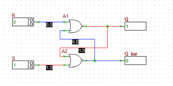
First, build the basic SR latch using two cross-coupled NOR gates as shown in the above figure. Before starting the simulation, manually set the inputs as S = 1 and R = 0. This is the "SET" state of the latch. Run a live digital simulation by manual stepping. Click the "Step" ![]() button of the Main Toolbar or simply use the keyboard shortcut "Ctrl+H". Note that the Q output changes to 1, while its complement Q_bar changes to 0. Change S to 0. Now, you have S = R = 0. This is the "HOLD" state. Step the simulation, and you will note that the output do not change at this state. Now change R to 1, while S is still at 0. This is the "RESET" state of the latch. Step the simulation and you will see that Q changes to 0 and Q_bar turns 1.
button of the Main Toolbar or simply use the keyboard shortcut "Ctrl+H". Note that the Q output changes to 1, while its complement Q_bar changes to 0. Change S to 0. Now, you have S = R = 0. This is the "HOLD" state. Step the simulation, and you will note that the output do not change at this state. Now change R to 1, while S is still at 0. This is the "RESET" state of the latch. Step the simulation and you will see that Q changes to 0 and Q_bar turns 1.
The truth table of the basic NOR SR latch is given below:
|
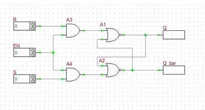
Next, you will add an "Enable" input to your SR latch using two AND gates as shown in the opposite figure. The EN input is fed into both AND gates. Therefore, as long as EN =0, the output of both AND gates is 0. This leads to S = R = 0, which represents the Hold state of the basic NOR SR latch. Before you start the simulation, set EN = 0. Then, set S = 1 and R = 0. Start a live digital simulation by manual stepping. Unlike the previous case, the output Q and Q_bar do not change this time. Next, set EN = 1. step the simulation and you will see that outputs change to Q = 1 and Q_bar = 0 (Set state). While EN = 1, change to S = 0 and R = 1. Step through and the gated latch enters its Reset sate with Q = 0 and Q_bar = 1.
The truth table of the gated NOR SR latch is given below:
|
Verifying B2.Spice's SR Latch Device
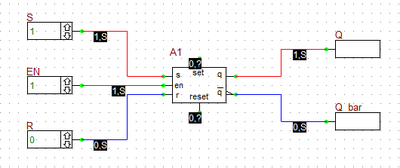
Next, you will remove the two NOR and two AND gates from you digital circuit and replace the four gates with an SR latch device. Connect the input S and R pins and output Q and Q_bar outputs pins of the device as shown in the figure below. Note that unlike the previous circuit, here the top and bottom inputs are called S and R, respectively. Repeat the same procedure in the last part and change the values of the three inputs S, R, and EN in the same manner. You should be able to reproduce the above truth table for this circuit, too.


