Difference between revisions of "Analog Tutorial Lesson 13: Analyzing the Frequency Response of Multistage BJT Amplifiers"
Kazem Sabet (Talk | contribs) (→Replacing the BJT Models in Your Circuit) |
Kazem Sabet (Talk | contribs) (→Replacing the BJT Models in Your Circuit) |
||
| Line 177: | Line 177: | ||
</tr> | </tr> | ||
</table> | </table> | ||
| + | |||
| + | == Exploiting Negative Feedback == | ||
| + | |||
| + | Negative feedback is often used to extended the frequency response of amplifiers. In this part of the tutorial lesson, you will use the circuit of the previous part with your updated BJT models, and will modify it by adding negative feedback from the output to the input of the amplifier. For this purpose, detach the capacitor C5 from the ground and feed it back to the input with a series resistor RF = 25kΩ as shown in the figure below: | ||
<table> | <table> | ||
| Line 185: | Line 189: | ||
</tr> | </tr> | ||
</table> | </table> | ||
| + | |||
| + | Get the frequency response of the new updated amplifier circuit using the Bode Plotter. Click the {{key|Run sweep}} button and you will see the plot shown in the figure below. Note that the frequency response of the new amplifier has been significantly extended and its 3dB rolloff frequency is now about 4.7MHz with the imported BJT models. Also, note that the gain of the two-stage amplifier has dropped from 80dB to 60dB. This can be explained by the fact that the forward beta (bf) parameter of 2N2222 was 150, while the new BJT model has a reduced value of bf = 50. | ||
<table> | <table> | ||
Revision as of 04:37, 16 October 2015
Contents
What You Will Learn
In this tutorial you will build and test two-stage common emitter amplifiers using different BJT devices and examine their frequency response. You will learn how to import an external device model and use it in your circuit. You will also become familiar with RF.Spice's Bode Plotter virtual instrument.
Building a Two-Stage BJT Amplifier & Examining Its DC Bias
The following is a list of parts needed for this part of the tutorial lesson:
| Part Name | Part Type | Part Value |
|---|---|---|
| Vcc | Vcc DC Bias Source | DC, 15 |
| VS | Voltage Source | AC Amplitude = 1mV, Phase = 0 |
| R1 | Resistor | 200k |
| R2 | Resistor | 50k |
| R3 | Resistor | 12k |
| R4 | Resistor | 3.6k |
| R5 | Resistor | 120k |
| R6 | Resistor | 30k |
| R7 | Resistor | 6.8k |
| R8 | Resistor | 3.6k |
| RS | Resistor | 150 |
| RL | Resistor | 10k |
| C1 - C3 | Capacitor | 10u |
| C4 | Capacitor | 15u |
| C5 | Capacitor | 25u |
| Q1 - Q2 | Q2N2222 NPN BJT | Defaults |
| IN, OUT | Voltage Probe Marker | N/A |
In this tutorial lesson, you will analyze a two-stage common emitter amplifier. Place and connect all the parts as shown in the figure below:
The voltage source VS is an small-signal AC source with a peak amplitude of 1mV. Let's first take a look at the DC bias of the amplifier. You can run a DC Bias Test of your amplifier to find the operating point parameters of Q1 and Q2. Or you may simply run a live simulation of your circuit and enable circuit animation using "Show Voltage Text". The figure below shows the DC voltage at the operating point:
Using a Bode Plotter Virtual Instrument
In Tutorial Lesson 3, you ran an AC Frequency Sweep to get the frequency response of your simple BJT amplifier. You can certainly do the same thing here, too. However, RF.Spice A/D provides a quick virtual instrument for this purpose. It is called the Bode Plotter and you can place one from the Instrument Panel on the right side of the screen. First, you have to set up your virtual instrument. Click the Setup button and open the Input/Output tab of the drop-down panel. Set your input between Nodes 0 and 1 and set your output between Nodes 10 and 0. Set the Signal Amplitude equal to 1mV and keep the default zero value of Signal Offset. In the Sweep tab of the drop-down panel, set the Start and Stop frequencies to 10Hz and 20MHz, respectively. Set the value of Step / Interval equal to 50 and choose the "Decade" option for Interval Type.
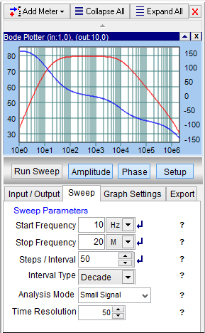
You are now set!! Click the Run Sweep button of the instrument, and the frequency response is immediately plotted. Note the Bode Plotter, by default, plots the gain of your circuit define as V(out)/V(in). As you can see from the figure below, your two-stage amplifier provide a high gain of 80dB, but the frequency response rolls off below 10kHz. Your amplifier cannot be used for higher frequencies!
Importing a New BJT Model
In the previous part, you picked a commercial BJT part from RF.Spice's extensive parts database. In many cases, you may need to use a new device model that doesn't already exist in RF.Spice's database. You can define a new device model from the ground up, or you may import new device models from external text files. In RF.Spice A/D, a device or part is the combination of a simulation or process model and a symbol. You can build a complete new device and store it to the parts database. You can also use an existing part and simply change the model behind it.
In this part of the tutorial lesson, you are going to import a new BJT model from a text file called "MyBJTModel.TXT". Open a blank text file using any text editor such as Windows Notepad and type in the following text ad save it to the file:
. model MyBJTModel npn
Next, open the RF.Spice A/D Device Manager using the keyboard shortcut Ctrl+D. Open the menu item Menu > File > Import Model from Text File… Follow the instructions on the screen. Enter the model name and a description for your new model such as "New NPN-type BJT model". Use the Windows Explorer's Open Dialog to browse your folders, locate the model text file and open it. The program will prompt that your new model has been added to the database.
Replacing the BJT Models in Your Circuit
Next, go back to the circuit of the previous part. Open the property dialog of the transistor Q1 and click the New Model button of that dialog. the Select Model Dialog opens up where you can search for "MyNewBJTModel". Note that the process devices such as BJTs share the same model by default. Therefore, once you change the model of Q1, the model of Q2 will also change and get updated. Run a new live simulation of your circuit to examine its DC bias. As you can see from the figure below, the collector and emitter voltages of both Q1 and Q2 have changed compared to the previous part.
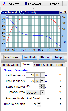
Get the frequency response of the new updated amplifier circuit using the Bode Plotter. Click the Run sweep button and you will see the plot shown in the figure below. Note that the frequency response of the new amplifier has been significantly extended and its 3dB rolloff frequency is now about 4.7MHz with the imported BJT models. Also, note that the gain of the two-stage amplifier has dropped from 80dB to 60dB. This can be explained by the fact that the forward beta (bf) parameter of 2N2222 was 150, while the new BJT model has a reduced value of bf = 50.
Exploiting Negative Feedback
Negative feedback is often used to extended the frequency response of amplifiers. In this part of the tutorial lesson, you will use the circuit of the previous part with your updated BJT models, and will modify it by adding negative feedback from the output to the input of the amplifier. For this purpose, detach the capacitor C5 from the ground and feed it back to the input with a series resistor RF = 25kΩ as shown in the figure below:
Get the frequency response of the new updated amplifier circuit using the Bode Plotter. Click the Run sweep button and you will see the plot shown in the figure below. Note that the frequency response of the new amplifier has been significantly extended and its 3dB rolloff frequency is now about 4.7MHz with the imported BJT models. Also, note that the gain of the two-stage amplifier has dropped from 80dB to 60dB. This can be explained by the fact that the forward beta (bf) parameter of 2N2222 was 150, while the new BJT model has a reduced value of bf = 50.
In the above figure, p(vcc) is the DC power of the DC power supply VCC, while p(rl) is the power delivered to the load. The ratio p(rl)/p(vcc) defines the power efficiency of the amplifier. From the above plots, you can read the peak-to-peak input and output voltages, voltage gain and power efficiency:
| RL | Vin(p-p) | Vout(p-p) | Voltage Gain | IRL(p-p) | PVCC | PRL | Power Efficiency |
|---|---|---|---|---|---|---|---|
| 10kΩ | 1686mV | 200mV | 8.43 | 168.5μA | 15.68mW | 71.28μW | 0.46% |


