| Tutorial Project: Modeling Periodic Frequency Selective Surfaces
|

|
|
Objective: In this project, you will build and analyze a periodic planar structure illuminated by a plane wave source.
|
|
Concepts/Features:
- CubeCAD
- Periodicity
- Plane Wave Source
- Reflection Coefficient
- Transmission Coefficient
- Oblique Incidence
|
|
Minimum Version Required: All versions
|
|
' Download Link: [1] Download Link: [1]
|
Objective:
To construct a periodic planar structure in EM.Cubeâs Planar Module, excite it with a plane wave source and compute its reflection and transmission characteristics.
What You Will Learn:
In this tutorial lesson you will use EM.Cube's spectral domain periodic Planar MoM simulation engine and will learn how to define plane wave sources.
Getting Started
Open the EM.Cube application and switch to Planar Module. Start a new project with the following attributes:
- Name: PMOMLesson5
- Length Units: mm
- Frequency Units: GHz
- Center Frequency: 9GHz
- Bandwidth: 14GHz
- Number of Finite Substrate Layers: 1
- Top Half-Space: Vacuum
- Middle Layer: ROGER RT/Duroid 5880, εr = 2.2, μr = 1, Ï = Ïm = 0, thickness = 6mm
- Bottom Half-Space: Vacuum
Drawing the Periodic Unit Cell
Define a PEC group called PEC_1 and draw a rectangle strip of dimensions 3mm à 12mm. Open the Periodicity Dialog of the Planar Module by right-clicking on the "Periodicity" item of the Navigation Tree and selecting "Periodicity Settings..." from the contextual menu. Check the box labeled "Periodic Structure" and set the "Spacing" equal to 15mm along both X and Y directions. Leave the "Offset" boxes with their default zero values.
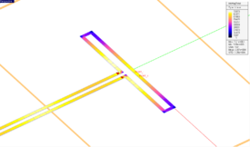
 The geometry of the Wilkinson power divider without the lumped resistor. |
 The property dialog of the Circle Strip object. |

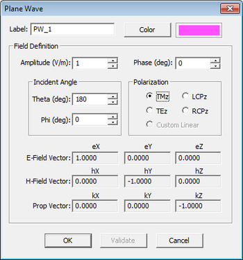
The Plane Wave Source dialog.
Defining a Plane Wave Source
Plane wave source are used to illuminate and excite periodic surfaces and compute their reflection and transmission characteristics. To define a plane wave source, right-click on the "Plane Waves" item of the Navigation Tree and select "Insert New Source..." from the contextual menu. This opens up the Plane Wave Source dialog. By default, a downward-looking normally incident plane wave source is assumed. This corresponds to incident Theta and Phi angles of 180° and 0°, respectively. Also, the default polarization of plane wave source is "TMz". You can also choose "TEz" or circular polarizations RCPz and LCPz.
 |
In EM.Cube, the incident angles of a plane wave source correspond to its propagation vector.
|
For this part of the tutorial lesson, you will start with the default plane wave source and then change its polarization as well as its incident Theta and Phi angles.

The geometry of the Wilkinson power divider without the lumped resistor.
Running a Planar MoM Analysis
Set the planar mesh density to 30 cells per effective wavelength. View and inspect the generated mesh. Also define a default current distribution observable.
 |
If your structure is periodic and excited by a plane wave source, EM.Cube always computes its reflection and transmission coefficients without a need to define an observable.
|
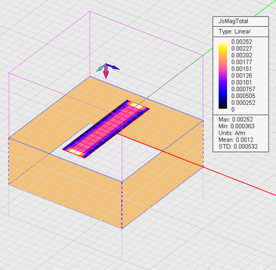
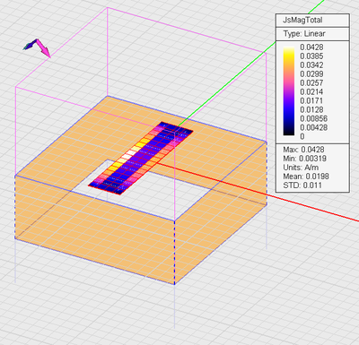
Run a quick planar MoM analysis of your periodic planar surface. At the end of the simulation, read the values of the computed reflection and transmission coefficients in the output message window. Also visualize the current distribution of the surface of the strip. Repeat this procedure for the following combination of source polarization and incident Theta and Phi angles:
|
|
| Source Case
|
Polarization
|
Theta
|
Phi
|
Reflection Coefficient
|
Transmission Coefficient
|
| 1
|
TMz
|
180°
|
0°
|
-0.369501 + 0.0143261j
|
-0.124906 - 0.920686j
|
| 2
|
TEz
|
180°
|
0°
|
-0.908299 - 0.222347j
|
-0.344712 - 0.0820254j
|
| 3
|
TEz
|
135°
|
0°
|
-0.963313 + 0.103053j
|
0.0409091 - 0.11252j
|
| 4
|
TEz
|
135°
|
45°
|
-0.781353 - 0.0441467j
|
-0.165279 - 0.48628j
|
 Electric field distribution on periodic strip with a TMz-polarized plane wave source: θ = 180° and Ï = 0°. |
 Electric field distribution on periodic strip with a TEz-polarized plane wave source: θ = 180° and Ï = 0°. |
 Electric field distribution on periodic strip with a TEz-polarized plane wave source: θ = 135° and Ï = 0°. |
 Electric field distribution on periodic strip with a TEz-polarized plane wave source: θ = 135° and Ï = 45°. |
Create a PEC group on the Navigation Tree and call it PEC_1. Draw six rectangle strip objects with dimensions and locations given in the table below:
S11(dB): -14.158286
S21(dB): -3.119946
S31(dB): -3.194342
S22(dB): -6.227977
S33(dB): -6.094034
S32(dB): -7.046050
Also, visualize the current distribution on the divider circuit. Note that the maximum current on Port 1 line is about 40A/m, while the maximum current values on the Port 2 and Port 3 lines are about 28V/m as expected (40 / â2 â
28).
Adding a Lumped Resistor
From the computed S-parameters above, you notice that Port 2 and 3 are not well matched. Moreover, there is strong coupling between these two ports (|S32| â
-6dB). In this part of the tutorial lesson, you will add a lumped resistor between the two output ports of your power divider to complete the Wilkinson design. But first you need to draw a line segment between the two objects Rect2 and Rect3 to hold the lumped element. Draw a new rectangle strip object of dimensions 1mm à 5mm centered at (19mm, 0, 0787mm).
 |
Just like gap sources, lumped elements require a host line object, and can only be defined in association with an existing rectangle strip object.
|
S11(dB): -13.045753
S21(dB): -3.216099
S31(dB): -3.181815
S22(dB): -6.174566
S33(dB): -6.262623
S32(dB): -4.653520
S33: -0.080736 +0.479511j
frequency sweep of your folded slot antenna to examine its frequency response and resonance behavior. Keep in mind that an adaptive frequency sweep does not generate current distribution plots or 3D radiation patterns at each frequency sample, but a uniform frequency sweep does. Therefore, first run a uniform frequency sweep with the following parameters:
Start Frequency: 1.4GHz
End Frequency: 2.0GHz
Number of Frequency Samples: 13
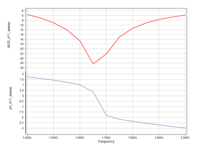
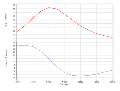
You will see that around 1.65GHz, the imaginary part of Z11 (i.e. input reactance) vanishes. Additionally, around the same frequency, the magnitude of S11 (return loss) dips into a deep minimum. This a good sign that your antenna both is both resonant and impedance-matched at that frequency.
 The graphs of S 11 as a function of frequency |
 The graphs of Z 11 as a function of frequency |
The figures below show the magnetic current distributions on the slot antenna and its CPW feed line at three different frequencies: 1.4GHz (left), 1.65GHz (middle) and 1.85GHz (right).
 The magnetic current distributions on the slot antenna and its CPW feed line at 1.4GHz (left), 1.65GHz (middle) and 1.85GHz
Next, run an adaptive frequency sweep with the following parameters:
Start Frequency: 1.4GHz
End Frequency: 2.0GHz
Min No. of Frequency Samples: 5
Max No. of Frequency Samples: 15
Convergence Criterion: 0.02
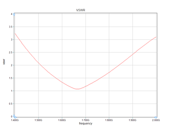
At the end of the adaptive sweep, graph the data files âS11_RationalFit.CPXâ and âZ11_RationalFit.CPXâ in EM.Grid. From the S11 and Z11 graphs you can see that the actual resonant frequency is about 1.665GHz. You can also check the voltage standing wave ration of your antenna structure by graphing the file âVSWR_RationalFit.DATâ. In this graph, you can see the minimum VSWR value of 1.06. The two red horizontal lines mark VSWR = 1.0 and VSWR = 1.5.
 The graph of S 11 as a function of frequency (adaptive) |
 The graph of Z 11 as a function of frequency (adaptive) |
 The plot of voltage standing wave ratio |
Back to EM.Cube Wiki Main Page
|
Last modified on 28 October 2014, at 19:14
