Analog Tutorial Lesson 4: Analyzing CMOS Logic Circuits
Analyzing CMOS Logic Circuits
Contents
Objective
In this tutorial lesson, first you will build and analyze three logic gate circuits: an inverter, a two-input NAND gate and a two-input NOR gate, using complementary MOSFET transistors. Then you will combine the previous circuits to build a two-input AND gate and a two-input OR gate.
Building a Basic CMOS Inverter
The following is a list of parts needed for this project:
DC Voltage Source V1: 1V
DC Voltage Source V2: 5V
MOSFET M1: N-Type (Keyboard Shortcut: M)
MOSFET M2: P-Type (Keyboard Shortcut: Alt+M)
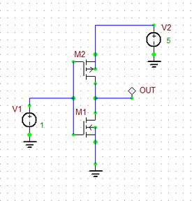
Connect the drain pin of the N-type MOSFET M1 to the source pin of the P-type MOSFET M2 to create a complementary MOS (CMOS) pair. Ground the source pin of M1 and connect the drain pin of M2 to the 5V voltage source V2. Connect the gate pins of both MOSFETs to each other and then connect them to the input voltage source V1. Connect the bulk pins of M1 and M2 to their source pins, respectively, as shown in the figure.
The output of the circuit will be at the drain pin of M1 or the source pin of M2. You can place a voltage marker at this location to mark it as the output.
Testing the CMOS Inverter Using Live Parameters
Your CMOS circuit is ready to run at this time. First, you will run a quick "Live Simulation" with Circuit Animation. In this tutorial lesson you will use the "Live Parameters" feature of B2.Spice A/D. Go to the Toolbox side panel on the left of the screen and click on its "Parameters" tab. At the top of the panel, choose the "Some" option to answer the question "How many parameters?". In the parameter table, the parameter "v1.tran_dc" represent the current voltage of the DC source V1, which must be 1V at this time.
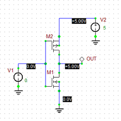
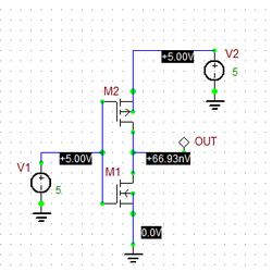
Click the "Go/Run" ![]() button of the Main Toolbar to start the live simulation. Animate the circuit by clicking the "Show Voltage Text" button (with the letter V) on the Schematic Toolbar. You will see that an output voltage of 4.85V is displayed on the schematic. The 1V input voltage is not a representative binary voltage. We will use 0V for the "Low" state and 5V for the "High" state. While the live simulation is still running, go the Parameters tab of the Toolbox, select the "v1.tran_dc" parameter, and type in the value "0" at the top of the panel. Make sure to press the "Down Arrow" or "Enter" button to make your change effective. The output voltage changes to 5V. Next, type in a value of "3" volts for the input. The output voltage drops to 763.93mV. Finally, enter "5" volts, and output voltage drops to almost zero.
button of the Main Toolbar to start the live simulation. Animate the circuit by clicking the "Show Voltage Text" button (with the letter V) on the Schematic Toolbar. You will see that an output voltage of 4.85V is displayed on the schematic. The 1V input voltage is not a representative binary voltage. We will use 0V for the "Low" state and 5V for the "High" state. While the live simulation is still running, go the Parameters tab of the Toolbox, select the "v1.tran_dc" parameter, and type in the value "0" at the top of the panel. Make sure to press the "Down Arrow" or "Enter" button to make your change effective. The output voltage changes to 5V. Next, type in a value of "3" volts for the input. The output voltage drops to 763.93mV. Finally, enter "5" volts, and output voltage drops to almost zero.
Characterizing the CMOS Inverter Through DC Sweep Test
In Tutorial Lesson 3, you already analyzed an RTL inverter using a BJT transistor and explored its DC response. You should expect a similar DC response from your CMOS circuit in this tutorial lesson. Bring up the Test Panel, select the "DC Sweep" option and open the Test Setup Dialog. Enter the following sweep parameters:
Source: V1
Property: DC
Start Value: 0
End Value: 5.0
Step Value: 20m
If you already placed a voltage probe called "OUT" at the output of your circuit as indicated in the above figure, then v(OUT) must already be in the list of the "Preset Graph Plots". So you do not need to introduce any additional plots. Run the basic DC Sweep Test, and you will get a response curve like the one shown below.
Building and Testing CMOS NAND and NOR Gate Circuits
The following is a list of parts needed for this part of the tutorial lesson:
DC Voltage Sources V1 and V2: 1V
DC Voltage Source VSS: 5V
Two N-Type MOSFETs: M1 and M2
Two P-Type MOSFETs: M3 and M4
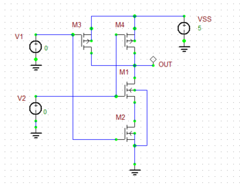
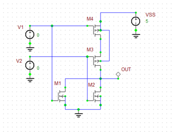
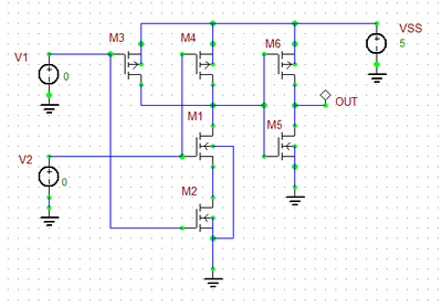
The figures below show the CMOS NAND and NOR logic gate circuits with two inout voltage sources v1 and v2. Build these circuits in two separate projects. Connect the various pins of the four MOSFETs according to the given schematics. For most pins, you can simply drag a wire using the left mouse button. For some other connections you need to use the Wire Tool (keyboard shortcut: Ctrl+W). Note that in the NAND circuit, the bulk pins of M2, M3 and M4 are connected to their respective source pins, while the bulk pin of M1 is connected to the bulk pin of M2. In the NOR circuit, the bulk pins of M1, M2 and M4 are connected to their respective source pins, while the bulk pin of M3 is connected to the bulk pin of M4. In the NAND circuit, the drains of the two P-type M3 and M4 and the drain of the N-type M1 are all connected to each other to provide the output node of the gate. In the NOR circuit, the drains of the two N-type M1 and M2 and the drain of the P-type M3 are all connected to each other to provide the output node of the gate.
Run live simulations of both circuits and use the Parameters panel of the Toolbox to vary the values of the two input voltages V1 and V2 during the simulations. Choose the binary voltage levels of 0V and 5V for the inputs and build and verify the truth table for each circuit as shown below:
| NAND | NOR | ||||||||||||||||||||||||||||||
|
|
Building and Testing CMOS AND and OR Gate Circuits
The following is a list of parts needed for this part of the tutorial lesson:
DC Voltage Sources V1 and V2: 1V
DC Voltage Source VSS: 5V
Three N-Type MOSFETs: M1, M2 and M5
Three P-Type MOSFETs: M3, M4 and M6
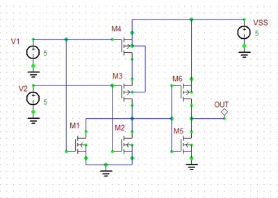
An AND logic gate can be built by cascading a NAND gate and an inverter. Similarly, an OR logic gate can be built by cascading a NOR gate and an inverter. At this part of the tutorial lesson, you will combine the CMOS inverter circuit of the first part with the CMOS NAND and NOR circuits of the second part to crate CMOS AND and OR gate circuits. The figures below show the schematic of the resulting gate circuits. You can place and connect the parts of these circuits from the ground up or you can copy and paste combinations of parts from the circuits you built earlier.
| |
In B2.Spice A/D you can open several circuit projects simultaneously. You can switch back and forth between the projects through the Window Menu. You can also cut, copy and paste among different projects. |
Run live simulations of both circuits and use the Parameters panel of the Toolbox to vary the values of the two input voltages V1 and V2 during the simulations. Similar to the previous part, build and verify the truth table for each circuit as shown below:
| AND | OR | ||||||||||||||||||||||||||||||
|
|
