What You Will Learn
In this tutorial you will use RF.Spice's black-box virtual blocks to model a Quadrature Amplitude Modulation (QAM) communication system and construct a pair of transmitter and receiver circuits. Then you will use a long lossy transmission line as the channel to connect the transmitter and receiver circuits. You will simulate the transmission of a binary data packet through this communication link.
Overview of the FMCW Radar System
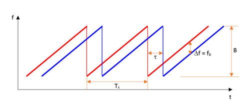
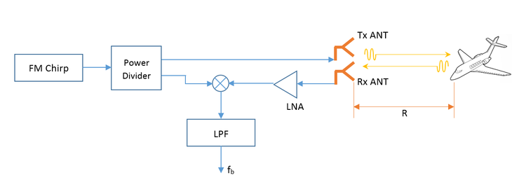
In an FMCW radar system, a chirp signal is launched into the free space using a transmit antenna. A chirp signal is an FM-modulated signal of a known stable frequency whose instantaneous frequency varies linearly over a fixed period of time (sweep time) by a modulating signal. The transmitted signal hits at the target and reflects back to a receive antenna. The frequency difference between the received signal and the transmitted signal increases with delay, and the delay is linearly proportional to the range, that is the distance of the target from the radar. The echo from the target is then mixed with the transmitted signal and down-converted to produce a beat signal which is linearly proportional to the target range after demodulation. The figure below shows the transmitted and received ramp signals:
The delay Ï is equal to the round-trip wave travel time and given by:
[math] \tau = \frac{2R}{c} [/math]
where R is the target range and c is the free-space speed of light. The beat frequency at the output of the receiver is given by:
[math] f_b = \frac{B}{T_s}\tau [/math]
where B is the total frequency deviation of the chirp signal and Ts is the sweep time (chirp period). The target range is thus found from the following equation:
[math] R = \frac{cT_s}{2B} f_b [/math]
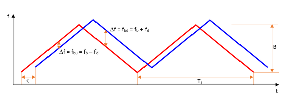
An FMCW radar system with a sawtooth chirp modulation can only measure the target's range but not its velocity if the target is moving. For that purpose, you need a triangular wave chirp modulation as shown in the figure below:
A moving target causes addition frequency shifting of the echo signal due to the Doppler effect, which can be expressed by the following relationship:
[math] f_{Rx} = f_{Tx} \left( \frac{1+v/{c}}{1-v/c} \right) [/math]
where fTx and fRx are the frequency of the transmitted and received signals respectively, and vr is the relative velocity of the target with respect to the radar system. The frequency shift due to the target's velocity is then given by:
[math] f_d = f_{Rx} - f_{Tx} = 2 f_{Tx}\frac{v_r}{c-v_r} \approx \frac{2v_r}{\lambda_0} [/math]
where and λ0 = c/f is the free=space wavelength, and it was assumed that vr << c.
[math] f_{bu} = f_b - f_d \\ f_{bd} = f_b + f_d [/math]
where fbu and fbd are the beat frequencies during the up-ramp and down-ramp sweeps, respectively. The target range and velocity are then calculated from the following equations:
[math] R = \frac{cT_s}{4B} \left( f_{bd} + f_{bu} \right) [/math]
[math] v_r = \frac{\lambda_0}{4} \left( f_{bd} - f_{bu} \right) [/math]
Exploring FM Modulation
The following is a list of parts needed for this part of the tutorial lesson:
| Part Name | Part Type | Part Value |
|---|---|---|
| V1 | Voltage Source | Waveform TBD |
| X1 | FM Modulator Block | Defaults |
| R1 | Resistor | 100 |
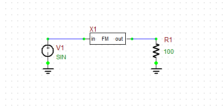
RF.Spice's FM modulator takes an arbitrary input signal and generates a frequency-modulated sinusoidal signal as its output. Place and connect the parts as shown in the figure below.
In this part of the lesson, you will use different waveforms as the input signal to the FM modulator. You can access the FM Modulator Block from Menu > Parts > Modulation Blocks > FM Modulator Block. The property dialog of this block is shown in the figure below. Set the Carrier Frequency to 10MHz and the Maximum Frequency Deviation to 5MHz.
You will use the basic voltage source V1 to generate a sinusoidal waveform. Then you will replace it with a Pulse Generator, a Ramp Generator and a Triangular Wave Generator, all of which can be accessed from Menu > Parts > Waveform Generator Blocks > Basic Waveforms. Define each source one by one according to the waveform tables below:
|
 Â
|
|
 Â
|
|
 Â
|
For each waveform, run a Transient Test of your modulator circuit with the following parameters:
The results are shown in the figures below for all the four different waveforms. Using the graph window's Delta Line Mode, you can measure the period of the FM-modulated waveforms at different time instants. You will find that when the input signal is zero, the period is 100ns (corresponding to 10MHz). When the input signal reaches +1V or -1V, the modulated output frequency increases to 15MHz or decreases to 5MHz, respectively.
In this part of the tutorial lesson, you will build a QAM demodulator circuit. To test your demodulator circuit, you will initially use an AM-modulated voltage source for the input signal. This source is accessible from Menu > Parts > Waveform Generation Blocks > Modulated Waveforms > Single-Tone AM Modulated Source. It represents a sinusoidal baseband signal of frequency fs modulated on a carrier frequency of fc. The AM waveform can be expressed as: [math] y(t) = A_c \left( 1 + m x(t) \right) cos(2\pi f_c t) = A_c \left( 1 + m A_s cos(2\pi f_s t) \right) cos(2\pi f_c t) [/math] where fc and fs are the carrier and signal frequencies, respectively, and m (the MDI parameter) is the modulation index or depth. m = 0 means no modulation, and m = 1 represent full modulation. You are going to feed an AM modulated signal with a signal frequency of 300MHz, a carrier frequency of 3GHz, a carrier amplitude of 15V and a modulation index of m = 1.
Place and connect all the parts as shown in the figure below. For the receiver circuit, instead of a Wilkinson power divider, you will use a simpler resistive power divider. Set the lengths of the input and output feed lines to a minimum: len_in = len_out = 2mm. For this part, you will use the "Limiter Block" simply as an amplifier with a gain of 5. For the peak detector block of the receiver circuit, you will use a full-wave bridge rectifier together with a simple RC filter. The analog binary output of this circuit fluctuates between low and high voltage levels. Finally, the Ideal Comparator Block compares the output of the peak detector circuit to a fixed DC voltage of +4V. Set the gain of the comparator to 10. This may also serve as an IF or baseband amplifier. The output of the comparator is converted to a digital output using s ADC bridge. Run a Transient Test of your modulator circuit with the following parameters:
The results are shown in the figure below. As you can see from the figure, the voltage signal v(7) at the output of the peak detector (plotted in dark blue) is a good reconstructed replica of the baseband 300MHz sinusoidal signal. Compare this signal to the envelope of the input AM-modulated signal plotted in yellow. You can use the "Delta Line Mode" of the graph window to measure the period or clock rate of the binary output, which is about 3.34ns consistent with the signal frequency of fs = 300MHz. Putting the Transmitter and Receiver Together With the ChannelThe following is a list of parts needed for this part of the tutorial lesson:
In this part of the tutorial lesson, you will put the QAM modulator and demodulator circuits of the previous parts together with a channel to simulate a communication link. In a wireless system, the channel is the free space between the transmit and receive antennas. One way of modeling the free-space channel in RF.Spice A/D is to use a dependent voltage source at the input of the receiver that is driven by the voltage at the output of the transmitter. The proportionality constant can be set to a very small number representing the free-space path loss. For this project, however, you will use a wired channel or cable represented by a lossy transmission line segment. In that case, the receiver can be directly connected to the output port of the T-Line segment. You will use a TEM line with Z0 = 50Ω, eeff = 1 and alpha = 0.5dB/m. At a length of 10m, the total single attenuation due to the channel will be 5dB. You are now ready to put it all together. This time you will send the QAM-modulated output of the transmitter circuit you built earlier through the transmission line channel and will feed it as the input of your receiver circuit. This signal will replace the AM-modulated voltage source you used in the previous section to feed your QAM demodulator circuit. For this part of the project, you will place an Ideal Buffer Block for isolation between the transmission line and the rest of the receiver circuit. The Limiter Block will both amplify and clip the signal from the top and bottom. Set the gain to 5 and set the lower and upper limits of the output voltage to -1V and +1V, respectively. Also define a gain of 5 for the Ideal Full-Wave Rectifier Block. Place and connect all the parts as shown in the figure below. Note that the part values of the peak detector's lowpass filter have changed from the previous part. Also, the reference voltage of the Ideal Comparator Block has been decreased to 2V. As the transmitted signal propagates through the transmission line, besides phase change or time delay, it also gets attenuated by 5dB over its whole length. The QAM-modulated signal signal arrives at the input of the receiver after a time delay equal to: [math] \Delta t = \frac{L}{c} = \frac{10m}{3\times 10^8 m/s} = 33.3ns [/math] To plan your Transient Test, keep in mind that the input binary sequence has a total duration of 20ns, of which the last 4ns are zeros (silent). In addition, the channel causes a time delay of 33.3ns. So choose the following parameters to run a Transient Test of your QAM data communications link:
The results are shown in the figure below. The plots in light and dark blue represent the voltage signals at the input and output of the long lossy transmission line. As you can from the figure, the demodulated signal at the digital output represents a fairly good replica of the input binary sequence. Â |


