Difference between revisions of "EM.Picasso"
m (→Probe Sources) |
|||
| Line 1: | Line 1: | ||
EM.Picasso® is a versatile planar structure simulator for modeling and design of printed antennas, planar microwave circuits, and layered periodic structures. EM.Picasso's simulation engine is based on a 2.5-D full-wave Method of Moments (MoM) formulation that provides the ultimate modeling accuracy and computational speed for open-boundary multilayer structures. It can handle planar structures with arbitrary numbers of metal layouts, slot traces, vertical interconnects and lumped elements interspersed among different substrate layers. You can use EM.Picasso to model large finite-sized antenna arrays as well as infinite periodic structures such as frequency selective surfaces. | EM.Picasso® is a versatile planar structure simulator for modeling and design of printed antennas, planar microwave circuits, and layered periodic structures. EM.Picasso's simulation engine is based on a 2.5-D full-wave Method of Moments (MoM) formulation that provides the ultimate modeling accuracy and computational speed for open-boundary multilayer structures. It can handle planar structures with arbitrary numbers of metal layouts, slot traces, vertical interconnects and lumped elements interspersed among different substrate layers. You can use EM.Picasso to model large finite-sized antenna arrays as well as infinite periodic structures such as frequency selective surfaces. | ||
| − | Since its introduction in 2002, EM.Picasso has been successfully used by numerous users around the globe in industry, academia and government. The new EM.Picasso 2013 has been totally reconstructed based on our integrated EM.Cube software foundation. This integration has introduced far more powerful CAD utilities, greater geometrical variety, and a vast array of capabilities like parametric sweep, [[optimization]], data visualization and post-processing computations. The new foundation also facilitates import and export of many popular CAD formats and provides a seamless interface with our other simulation tools. | + | Since its introduction in 2002, EM.Picasso has been successfully used by numerous users around the globe in industry, academia and government. The new EM.Picasso 2013 has been totally reconstructed based on our integrated [[EM.Cube]] software foundation. This integration has introduced far more powerful CAD utilities, greater geometrical variety, and a vast array of capabilities like parametric sweep, [[optimization]], data visualization and post-processing computations. The new foundation also facilitates import and export of many popular CAD formats and provides a seamless interface with our other simulation tools. |
== A Planar Method Of Moments Primer == | == A Planar Method Of Moments Primer == | ||
| Line 7: | Line 7: | ||
The Method of Moments (MoM) is a rigorous, full-wave numerical technique for solving open boundary electromagnetic problems. Using this technique, you can analyze electromagnetic radiation, scattering and wave propagation problems with relatively short computation times and modest computing resources. The method of moments is an integral equation technique; it solves the integral form of Maxwell’s equations as opposed to their differential forms that are used in the finite element or finite difference time domain methods. | The Method of Moments (MoM) is a rigorous, full-wave numerical technique for solving open boundary electromagnetic problems. Using this technique, you can analyze electromagnetic radiation, scattering and wave propagation problems with relatively short computation times and modest computing resources. The method of moments is an integral equation technique; it solves the integral form of Maxwell’s equations as opposed to their differential forms that are used in the finite element or finite difference time domain methods. | ||
| − | In a planar MoM simulation, the background structure is usually a layered planar structure that consists of one or more laterally infinite material layers. In EM. | + | In a planar MoM simulation, the background structure is usually a layered planar structure that consists of one or more laterally infinite material layers. In [[EM.Cube]]’s [[Planar Module]], the layered structure is stacked along the Z axis. In other words, the dimensions of the layers are infinite along the X and Y axes. Metallic traces are placed at the boundaries between the substrate or superstrate layers. These are modeled by perfect electric conductor (PEC) traces or conductive sheet traces of finite thickness and finite conductivity. Some layers might be separated by infinite perfectly conducting ground planes. The two sides of a ground plane can be electromagnetically coupled through one or several slots or apertures. Such slots or apertures are modeled by magnetic currents and are realized and represented by perfectly magnetic conductor (PMC) traces. Furthermore, the metallic traces can be interconnected or connected to ground planes using embedded objects. Such objects can be used to model circuit vias, plated-through holes or dielectric inserts. These are modeled as volume polarization currents. |
The currents in a planar MoM simulation are discretized as a collection of elementary currents with small finite spatial extents. These elementary currents are called basis functions and obviously have a vectorial nature. The total currents (solution of the problem) are summations of these elementary currents. The basis functions are well defined and easy to calculate; however, their amplitudes are initially unknown in a MoM problem. Through the planar MoM solution, you find these unknown amplitudes. Once the total currents are known, you can calculate the fields everywhere in the structure. | The currents in a planar MoM simulation are discretized as a collection of elementary currents with small finite spatial extents. These elementary currents are called basis functions and obviously have a vectorial nature. The total currents (solution of the problem) are summations of these elementary currents. The basis functions are well defined and easy to calculate; however, their amplitudes are initially unknown in a MoM problem. Through the planar MoM solution, you find these unknown amplitudes. Once the total currents are known, you can calculate the fields everywhere in the structure. | ||
| Line 51: | Line 51: | ||
Given the fact that the dyadic Green’s functions and the incident or impressed fields are all known, one can solve the above system of integral equations to find the unknown currents '''J''' and '''M'''. | Given the fact that the dyadic Green’s functions and the incident or impressed fields are all known, one can solve the above system of integral equations to find the unknown currents '''J''' and '''M'''. | ||
| − | In EM.CUBE's [[Planar Module|Planar module]], magnetic currents are always surface current with units of V/m. Electric currents, however, can be surface currents with units of A/m as in the case of metallic traces like microstrip lines, or they can be volume currents with units of A/m<sup>2</sup> as in the case of perfectly conducting vias. Dielectric inserts are modeled as volume polarization currents that are related to the electric field '''E''' in the following manner: | + | In [[EM.Cube|EM.CUBE]]'s [[Planar Module|Planar module]], magnetic currents are always surface current with units of V/m. Electric currents, however, can be surface currents with units of A/m as in the case of metallic traces like microstrip lines, or they can be volume currents with units of A/m<sup>2</sup> as in the case of perfectly conducting vias. Dielectric inserts are modeled as volume polarization currents that are related to the electric field '''E''' in the following manner: |
:<math>\mathbf{J}_p(r) = jk_0 Y_0(\varepsilon_r - \varepsilon_b)\mathbf{E}(r)</math> | :<math>\mathbf{J}_p(r) = jk_0 Y_0(\varepsilon_r - \varepsilon_b)\mathbf{E}(r)</math> | ||
| Line 60: | Line 60: | ||
=== Numerical Solution Of Integral Equations === | === Numerical Solution Of Integral Equations === | ||
| − | The planar integral equations derived earlier can be solved numerically by discretizing the unknown currents using a proper meshing scheme. The original functional equations are reduced to discretized linear algebraic equations over elementary cells. The unknown quantities are found by solving this system of linear equations, and many other parameters can be computed thereafter. This method of numerical solution of integral equations is known as the Method of Moments (MoM). In this method, the unknown electric and magnetic currents are represented by expansions of basis functions as follows: | + | The planar integral equations derived earlier can be solved numerically by discretizing the unknown currents using a proper meshing scheme. The original functional equations are reduced to discretized linear algebraic equations over elementary cells. The unknown quantities are found by solving this system of linear equations, and many other [[parameters]] can be computed thereafter. This method of numerical solution of integral equations is known as the Method of Moments (MoM). In this method, the unknown electric and magnetic currents are represented by expansions of basis functions as follows: |
:<math>J(r) = \sum_{n=1}^N I_n^{(J)} f_n^{(J)} (r)</math> | :<math>J(r) = \sum_{n=1}^N I_n^{(J)} f_n^{(J)} (r)</math> | ||
| Line 128: | Line 128: | ||
[[File:PMOM14.png|thumb|350px|A typical planar layered structure]] | [[File:PMOM14.png|thumb|350px|A typical planar layered structure]] | ||
| − | EM. | + | [[EM.Cube]]’s [[Planar Module]] is intended for constructing and modeling planar layered structures. By a planar structure we mean one that contains a background substrate of laterally infinite extents, made up of one or more material layers all stacked up vertically along the Z axis. Objects of finite size are then interspersed among these substrate layers. This is somehow different than [[EM.Cube]]'s other computational modules, which are geared for handling arbitrary 3D structures. |
| − | In [[Planar Module]], the background structure, called "'''Layer Stack-up'''", may involve one or more material layers of infinite extents along the X and Y axes but of finite thickness along the Z axis. When you start a new project, the background structure has a single vacuum layer. The layer stack-up is always terminated from the top and bottom by two infinite half-spaces. The terminating half-spaces might be the free space, or a perfect conductor (PEC ground), or any material medium. Most planar structures used in RF and microwave applications such as microstrip-based components have a PEC ground at their bottom. EM.Cube's default stack-up has a vacuum top half-space and a PEC bottom half-space. Some structures like stripline components require two bounding PEC grounds at both top and bottom. | + | In [[Planar Module]], the background structure, called "'''Layer Stack-up'''", may involve one or more material layers of infinite extents along the X and Y axes but of finite thickness along the Z axis. When you start a new project, the background structure has a single vacuum layer. The layer stack-up is always terminated from the top and bottom by two infinite half-spaces. The terminating half-spaces might be the free space, or a perfect conductor (PEC ground), or any material medium. Most planar structures used in RF and microwave applications such as microstrip-based components have a PEC ground at their bottom. [[EM.Cube]]'s default stack-up has a vacuum top half-space and a PEC bottom half-space. Some structures like stripline components require two bounding PEC grounds at both top and bottom. |
| − | The finite-sized objects of a planar structure may include metal traces, slots and apertures, vertical vias and interconnects, or dielectric inserts including air voids inside the substrate layers. Metal traces are modeled as electric surface currents. These are planar [[Surface Objects|surface objects]], always parallel to the XY plane, that are defined on metal (PEC) traces and placed at the boundary (interface) plane between two substrate layers. Slots and apertures are modeled as magnetic surface currents on the surface of an infinite PEC plane and provide electromagnetic coupling between its top and bottom sides. These, too, are constructed using planar [[Surface Objects|surface objects]], always parallel to the XY plane, that are defined on slot (PMC) traces and placed at the boundary (interface) plane between two substrate layers. EM.Cube's [[Planar Module]] also allows prismatic objects that can be modeled by electric volume currents. These include vertical vias and dielectric inserts, and are called embedded object sets. [[Planar Module|Planar module]] does not allow construction of 3D CAD objects. Instead, you draw the cross section of prismatic objects as planar [[Surface Objects|surface objects]] parallel to the XY plane. EM.Cube then automatically extrudes these cross sections and constructs and displays 3D prisms over them. The prisms extend all the way across the thickness of the host substrate layer. | + | The finite-sized objects of a planar structure may include metal traces, slots and apertures, vertical vias and interconnects, or dielectric inserts including air voids inside the substrate layers. Metal traces are modeled as electric surface currents. These are planar [[Surface Objects|surface objects]], always parallel to the XY plane, that are defined on metal (PEC) traces and placed at the boundary (interface) plane between two substrate layers. Slots and apertures are modeled as magnetic surface currents on the surface of an infinite PEC plane and provide electromagnetic coupling between its top and bottom sides. These, too, are constructed using planar [[Surface Objects|surface objects]], always parallel to the XY plane, that are defined on slot (PMC) traces and placed at the boundary (interface) plane between two substrate layers. [[EM.Cube]]'s [[Planar Module]] also allows prismatic objects that can be modeled by electric volume currents. These include vertical vias and dielectric inserts, and are called embedded object sets. [[Planar Module|Planar module]] does not allow construction of 3D CAD objects. Instead, you draw the cross section of prismatic objects as planar [[Surface Objects|surface objects]] parallel to the XY plane. [[EM.Cube]] then automatically extrudes these cross sections and constructs and displays 3D prisms over them. The prisms extend all the way across the thickness of the host substrate layer. |
<!-- | <!-- | ||
| Line 141: | Line 141: | ||
=== Defining Layer Stack-Up === | === Defining Layer Stack-Up === | ||
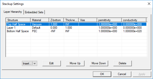
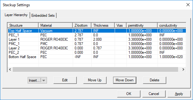
| − | When you start a new project in EM. | + | When you start a new project in [[EM.Cube]]’s [[Planar Module]], there is always a default background structure that consists of a finite vacuum layer sandwiched between a vacuum top half-space and a PEC bottom half-space. Every time you enter the [[Planar Module|Planar module]], the '''Stack-up Settings Dialog''' opens up. This is where you define the entire background structure. Once you close this dialog, you can open it again by right clicking the '''Layer Stack-up''' item in the '''Computational Domain''' section of the Navigation Tree and selecting '''Layer Stack-up Settings...''' from the contextual menu. Or alternatively, you can select the menu item '''Simulate > Computational Domain > Layer Stack-up Settings...''' |
The Stack-up Settings dialog has two tabs: '''Layer Hierarchy''' and '''Embedded Sets'''. The Layer Hierarchy tab has a table that shows all the background layers in hierarchical order from the top half-space to the bottom half-space. It also lists the material label of each layer, Z-coordinate of the bottom of each layer, its thickness (in project units) and material properties: permittivity (e<sub>r</sub>), permeability (µ<sub>r</sub>), electric conductivity (s) and magnetic conductivity (s<sub>m</sub>). There is also a column that lists the names of embedded object sets inside each substrate layer, if any. | The Stack-up Settings dialog has two tabs: '''Layer Hierarchy''' and '''Embedded Sets'''. The Layer Hierarchy tab has a table that shows all the background layers in hierarchical order from the top half-space to the bottom half-space. It also lists the material label of each layer, Z-coordinate of the bottom of each layer, its thickness (in project units) and material properties: permittivity (e<sub>r</sub>), permeability (µ<sub>r</sub>), electric conductivity (s) and magnetic conductivity (s<sub>m</sub>). There is also a column that lists the names of embedded object sets inside each substrate layer, if any. | ||
| Line 162: | Line 162: | ||
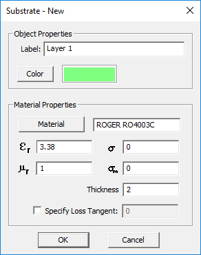
Figure 1: [[Planar Module]]'s Substrate Layer dialog. | Figure 1: [[Planar Module]]'s Substrate Layer dialog. | ||
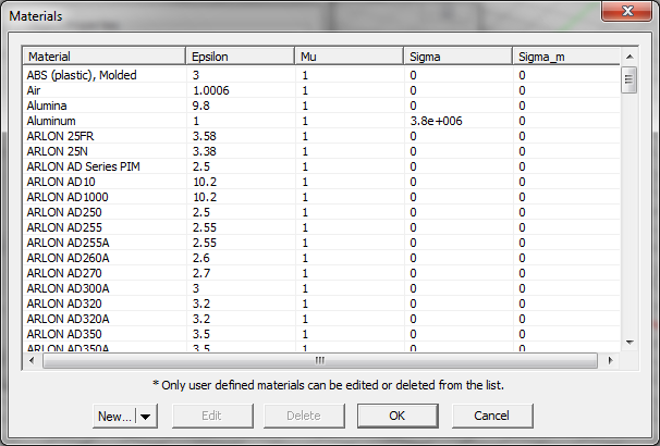
| − | You can also use EM.Cube's Material List to define the material properties of a substrate layer. In the Substrate Layer Dialog, click the '''Material''' button to open the '''Material List'''. In the Material List Dialog, pick any material or type the first letter of a material to highlight it. Then click the '''OK''' button or simply hit the '''Enter''' key of your keyboard to close the list and return to the substrate layer dialog. | + | You can also use [[EM.Cube]]'s Material List to define the material properties of a substrate layer. In the Substrate Layer Dialog, click the '''Material''' button to open the '''Material List'''. In the Material List Dialog, pick any material or type the first letter of a material to highlight it. Then click the '''OK''' button or simply hit the '''Enter''' key of your keyboard to close the list and return to the substrate layer dialog. |
[[File:PMOM10.png]] | [[File:PMOM10.png]] | ||
| − | Figure 2: EM.Cube's Materials dialog. | + | Figure 2: [[EM.Cube]]'s Materials dialog. |
=== Planar Object Types === | === Planar Object Types === | ||
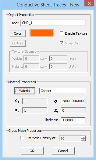
| − | EM. | + | [[EM.Cube]]’s [[Planar Module]] groups objects by their material and electromagnetic properties. Each object group shares the same color and same position in the layer stack-up. All the planar objects belonging to the same trace are located on the same substrate layer boundary. All the prismatic objects belonging to the same embedded set lie inside the same substrate layer and have the same material composition. Theoretically speaking, all the objects belonging to a group are governed by the same boundary conditions. [[EM.Cube]]’s [[Planar Module]] currently provides the following types of objects for building a planar layered structure: |
# '''Perfect Electric Conductor (PEC) Traces:''' These represent infinitesimally thin metallic objects that are deposited or metallized on or between substrate layers. PEC objects are modeled by surface electric currents that satisfy the PEC boundary condition. | # '''Perfect Electric Conductor (PEC) Traces:''' These represent infinitesimally thin metallic objects that are deposited or metallized on or between substrate layers. PEC objects are modeled by surface electric currents that satisfy the PEC boundary condition. | ||
| Line 200: | Line 200: | ||
[[File:PMOM13.png]] | [[File:PMOM13.png]] | ||
| − | EM.Cube's [[Planar Module]] has a special feature that makes construction of planar structures quite easy and straightforward. '''The active work plane of the project workspace is always set at the plane of the active trace.''' In EM.Cube's other modules, all objects are drawn in the XY plane (z = 0) by default. In [[Planar Module]], all new objects are drawn on a horizontal plane that is located at the Z-coordinate of the currently active trace. As you change the active trace or add a new trace, you will also change the active work plane. | + | [[EM.Cube]]'s [[Planar Module]] has a special feature that makes construction of planar structures quite easy and straightforward. '''The active work plane of the project workspace is always set at the plane of the active trace.''' In [[EM.Cube]]'s other modules, all objects are drawn in the XY plane (z = 0) by default. In [[Planar Module]], all new objects are drawn on a horizontal plane that is located at the Z-coordinate of the currently active trace. As you change the active trace or add a new trace, you will also change the active work plane. |
=== Modeling Metallic Traces === | === Modeling Metallic Traces === | ||
| Line 234: | Line 234: | ||
=== Modeling Slot Traces === | === Modeling Slot Traces === | ||
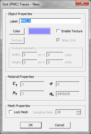
| − | Slots and apertures are cut-out and removed metal in an infinite perfectly conducting (PEC) ground plane. When a slot is excited, tangential electric fields are formed on the aperture, which can be modeled as finite magnetic surface currents confined to the area of the slot. Therefore, instead of modeling the electric surface currents on the PEC ground around the slot, one can alternatively model the finite-extent magnetic surface currents on PMC traces. In EM.Cube's [[Planar Module]], you define slot objects under PMC traces. A PMC trace at a certain Z-plane implies the presence of an infinite PEC plane at that Z-coordinate. Therefore, you do not need to define an additional PEC plane at that location on the layer stack-up. The slot (PMC) objects provide the electromagnetic coupling between the two sides of this infinite ground plane. By the same token, you cannot place a PEC trace and a PMC trace at the same Z-level, as the latter's ground will short the former. However, you can define two or more PMC traces at the same Z-plane. In this case, all the slot objects lie on the same infinite PEC ground plane. <br /> | + | Slots and apertures are cut-out and removed metal in an infinite perfectly conducting (PEC) ground plane. When a slot is excited, tangential electric fields are formed on the aperture, which can be modeled as finite magnetic surface currents confined to the area of the slot. Therefore, instead of modeling the electric surface currents on the PEC ground around the slot, one can alternatively model the finite-extent magnetic surface currents on PMC traces. In [[EM.Cube]]'s [[Planar Module]], you define slot objects under PMC traces. A PMC trace at a certain Z-plane implies the presence of an infinite PEC plane at that Z-coordinate. Therefore, you do not need to define an additional PEC plane at that location on the layer stack-up. The slot (PMC) objects provide the electromagnetic coupling between the two sides of this infinite ground plane. By the same token, you cannot place a PEC trace and a PMC trace at the same Z-level, as the latter's ground will short the former. However, you can define two or more PMC traces at the same Z-plane. In this case, all the slot objects lie on the same infinite PEC ground plane. <br /> |
[[File:PMOM20.png]] | [[File:PMOM20.png]] | ||
| Line 242: | Line 242: | ||
=== Defining Embedded Object Sets === | === Defining Embedded Object Sets === | ||
| − | Embedded object sets represent short material insertions inside substrate layers. They can be metal or dielectric. Metallic embedded objects can be used to model vias, plated-through holes, shorting pins and interconnects. These are called PEC via sets. Embedded dielectric objects can be used to model air voids, thin films and material inserts in metamaterial structures. Embedded magnetic object are not currently supported by EM. | + | Embedded object sets represent short material insertions inside substrate layers. They can be metal or dielectric. Metallic embedded objects can be used to model vias, plated-through holes, shorting pins and interconnects. These are called PEC via sets. Embedded dielectric objects can be used to model air voids, thin films and material inserts in metamaterial structures. Embedded magnetic object are not currently supported by [[EM.Cube]]’s [[Planar Module]]. |
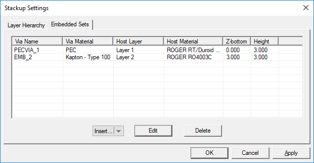
Embedded objects can be defined either from the Layer Stack-up Settings dialog or directly from the Navigation Tree. In the former case, open the "Embedded Sets" tab of the stack-up dialog. This tab has a table that lists all the embedded object sets along with their material type, the host substrate layer, the host material and their height. | Embedded objects can be defined either from the Layer Stack-up Settings dialog or directly from the Navigation Tree. In the former case, open the "Embedded Sets" tab of the stack-up dialog. This tab has a table that lists all the embedded object sets along with their material type, the host substrate layer, the host material and their height. | ||
| Line 252: | Line 252: | ||
Figure 1: [[Planar Module]]'s Layer Stack-up dialog showing the Embedded Sets tab. | Figure 1: [[Planar Module]]'s Layer Stack-up dialog showing the Embedded Sets tab. | ||
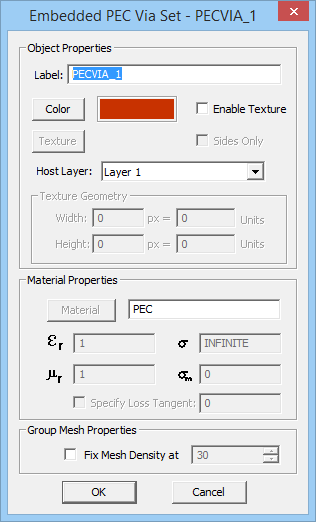
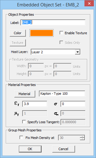
| − | To add a new object set, click the arrow symbol on the '''Insert''' button of the dialog and select one of the two options, '''PEC Via Set''' or '''Embedded Dielectric Set''', from the dropdown list. This opens up a new dialog where first you have to set the host layer of the new object set. A dropdown list labeled "'''Host Layer'''" gives a list of all the available finite substrate layers. You can also set the properties of the embedded object set, including its label, color and material properties. Keep in mind that you cannot control the height of embedded objects. Moreover, you cannot assign material properties to PEC via sets, while you can set values for the '''Permittivity'''(ε<sub>r</sub>) and '''Electric Conductivity'''(σ) of embedded dielectric sets. Vacuum is the default material choice. You may use EM.Cube's Material List for this purpose, which can be opened up by clicking the '''Material''' button. Once embedded object sets are added to the Embedded Sets table, you can edit their properties at any time by selecting their row and clicking the '''Edit''' button. | + | To add a new object set, click the arrow symbol on the '''Insert''' button of the dialog and select one of the two options, '''PEC Via Set''' or '''Embedded Dielectric Set''', from the dropdown list. This opens up a new dialog where first you have to set the host layer of the new object set. A dropdown list labeled "'''Host Layer'''" gives a list of all the available finite substrate layers. You can also set the properties of the embedded object set, including its label, color and material properties. Keep in mind that you cannot control the height of embedded objects. Moreover, you cannot assign material properties to PEC via sets, while you can set values for the '''Permittivity'''(ε<sub>r</sub>) and '''Electric Conductivity'''(σ) of embedded dielectric sets. Vacuum is the default material choice. You may use [[EM.Cube]]'s Material List for this purpose, which can be opened up by clicking the '''Material''' button. Once embedded object sets are added to the Embedded Sets table, you can edit their properties at any time by selecting their row and clicking the '''Edit''' button. |
[[File:PMOM21.png]] [[File:PMOM22.png]] | [[File:PMOM21.png]] [[File:PMOM22.png]] | ||
| Line 260: | Line 260: | ||
To define an embedded set from the Navigation Tree, right click on the '''Embedded Object Sets''' item in the '''Physical Structure''' section of the Navigation Tree and select either '''Insert New PEC Via Set...''' or '''Insert New Embedded Dielectric Set...''' The respective New Embedded Object Set dialog opens up, where you set the properties of the new object set. As soon as you close this dialog, it takes you to the Layer Stack-up Settings dialog, where you can examine the location of the new object set on the layer hierarchy. | To define an embedded set from the Navigation Tree, right click on the '''Embedded Object Sets''' item in the '''Physical Structure''' section of the Navigation Tree and select either '''Insert New PEC Via Set...''' or '''Insert New Embedded Dielectric Set...''' The respective New Embedded Object Set dialog opens up, where you set the properties of the new object set. As soon as you close this dialog, it takes you to the Layer Stack-up Settings dialog, where you can examine the location of the new object set on the layer hierarchy. | ||
| − | After a new embedded object set has been defined and added to the Navigation Tree, it becomes the active trace. You are now ready to create geometrical objects in the new active trace. Remember that [[Planar Module]] does not allow you to draw 3D objects. The solid object buttons in the '''Object Toolbar''' are disabled to prevent you from doing so. Instead, you draw planar [[Surface Objects|surface objects]] as the cross section of embedded sets. EM.Cube extends these planar objects across their host layer automatically and displays them as wire-frame, 3D extruded objects. Extrusion of embedded object sets happen after meshing and before every simulation. You can enforce this extrusion manually by right clicking the '''Layer Stack-up''' item in the '''Computational Domain''' section of the Navigation Tree and selecting '''Update Planar Structure...''' from the contextual menu. | + | After a new embedded object set has been defined and added to the Navigation Tree, it becomes the active trace. You are now ready to create geometrical objects in the new active trace. Remember that [[Planar Module]] does not allow you to draw 3D objects. The solid object buttons in the '''Object Toolbar''' are disabled to prevent you from doing so. Instead, you draw planar [[Surface Objects|surface objects]] as the cross section of embedded sets. [[EM.Cube]] extends these planar objects across their host layer automatically and displays them as wire-frame, 3D extruded objects. Extrusion of embedded object sets happen after meshing and before every simulation. You can enforce this extrusion manually by right clicking the '''Layer Stack-up''' item in the '''Computational Domain''' section of the Navigation Tree and selecting '''Update Planar Structure...''' from the contextual menu. |
=== Planar Module's Rules & Limitations === | === Planar Module's Rules & Limitations === | ||
| Line 269: | Line 269: | ||
# Metallic and slot traces are strictly defined at the interface planes between substrate layers. To define a suspended metallic trace in a substrate layer (as in the case of the center conductor of a stripline), you must split the dielectric layer into two thinner layers and place your PEC trace at the interface between them. | # Metallic and slot traces are strictly defined at the interface planes between substrate layers. To define a suspended metallic trace in a substrate layer (as in the case of the center conductor of a stripline), you must split the dielectric layer into two thinner layers and place your PEC trace at the interface between them. | ||
# The current version of the Planar MoM simulation engine is based on a 2.5-D MoM formulation. Only vertical volume currents and no circumferential components are allowed on embedded objects. The 2.5-D assumption holds very well in two cases: (a) when embedded objects are very thin with a very small cross section (with lateral dimensions less than 2-5% of the material wavelength) or (b) when embedded objects are very short and sandwiched between two closely spaced PEC traces or grounds from the top and bottom. | # The current version of the Planar MoM simulation engine is based on a 2.5-D MoM formulation. Only vertical volume currents and no circumferential components are allowed on embedded objects. The 2.5-D assumption holds very well in two cases: (a) when embedded objects are very thin with a very small cross section (with lateral dimensions less than 2-5% of the material wavelength) or (b) when embedded objects are very short and sandwiched between two closely spaced PEC traces or grounds from the top and bottom. | ||
| − | # The current release of EM.Cube allows any number of PEC via sets collocated in the same substrate layer. However, you can define only one embedded dielectric object set per substrate layer, and no vias sets collocated in the same layer. Note that the single set can host an arbitrary number of embedded dielectric objects of the same material properties. | + | # The current release of [[EM.Cube]] allows any number of PEC via sets collocated in the same substrate layer. However, you can define only one embedded dielectric object set per substrate layer, and no vias sets collocated in the same layer. Note that the single set can host an arbitrary number of embedded dielectric objects of the same material properties. |
=== Managing Objects, Traces & Sets === | === Managing Objects, Traces & Sets === | ||
| Line 275: | Line 275: | ||
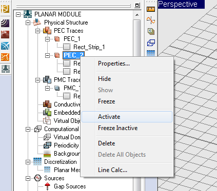
You can manage your project's layer hierarchy from the Layer Stack-up Settings dialog. You can add, delete and move around substrate layers, metallic and slot traces and embedded object sets. Metallic and slot traces can move among the interface planes between neighboring substrate layers. Embedded object sets including PEC vias and finite dielectric objects can move from substrate layer into another. When you delete a trace from the Layer Stack-up Settings dialog, all of its objects are deleted from the project workspace, too. You can also delete metallic and slot traces or embedded object sets from the Navigation Tree. To do so, right click on the name of the trace or object set in the Navigation Tree and select '''Delete''' from the contextual menu. You can also delete all the traces or object sets of the same type from the contextual menu of the respective type category in the Navigation Tree. | You can manage your project's layer hierarchy from the Layer Stack-up Settings dialog. You can add, delete and move around substrate layers, metallic and slot traces and embedded object sets. Metallic and slot traces can move among the interface planes between neighboring substrate layers. Embedded object sets including PEC vias and finite dielectric objects can move from substrate layer into another. When you delete a trace from the Layer Stack-up Settings dialog, all of its objects are deleted from the project workspace, too. You can also delete metallic and slot traces or embedded object sets from the Navigation Tree. To do so, right click on the name of the trace or object set in the Navigation Tree and select '''Delete''' from the contextual menu. You can also delete all the traces or object sets of the same type from the contextual menu of the respective type category in the Navigation Tree. | ||
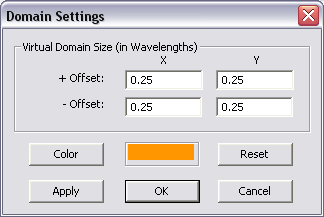
| − | For better visualization of your planar structure, EM.Cube displays a virtual domain in a default orange color to represent part of the infinite background structure. The size of this virtual domain is a quarter wavelength offset from the largest bounding box that encompasses all the finite objects in the project workspace. You can change the size of the virtual domain or its display color from the Domain Settings dialog, which you can access either by clicking the '''Computational Domain''' [[File:domain_icon.png]] button of the '''Simulate Toolbar''', or by selecting '''Simulate > Computational Domain > Domain Settings...''' from the Simulate Menu or by right clicking the '''Virtual Domain''' item of the Navigation Tree and selecting '''Domain Settings...''' from the contextual menu, or using the keyboard shortcut '''Ctrl+A'''. But keep in mind that the virtual domain is only for visualization purpose and does not affect the MoM simulation. The virtual domain also shows the substrate layers in translucent colors. As you change the colors assigned to the substrate layers, you will see a multilayer virtual domain box surrounding your project structure. | + | For better visualization of your planar structure, [[EM.Cube]] displays a virtual domain in a default orange color to represent part of the infinite background structure. The size of this virtual domain is a quarter wavelength offset from the largest bounding box that encompasses all the finite objects in the project workspace. You can change the size of the virtual domain or its display color from the Domain Settings dialog, which you can access either by clicking the '''Computational Domain''' [[File:domain_icon.png]] button of the '''Simulate Toolbar''', or by selecting '''Simulate > Computational Domain > Domain Settings...''' from the Simulate Menu or by right clicking the '''Virtual Domain''' item of the Navigation Tree and selecting '''Domain Settings...''' from the contextual menu, or using the keyboard shortcut '''Ctrl+A'''. But keep in mind that the virtual domain is only for visualization purpose and does not affect the MoM simulation. The virtual domain also shows the substrate layers in translucent colors. As you change the colors assigned to the substrate layers, you will see a multilayer virtual domain box surrounding your project structure. |
[[File:pmom_phys5.png]] | [[File:pmom_phys5.png]] | ||
| Line 281: | Line 281: | ||
Figure 1: [[Planar Module]]'s Virtual Domain Settings dialog. | Figure 1: [[Planar Module]]'s Virtual Domain Settings dialog. | ||
| − | By default, the last defined trace or embedded object set is active. You can activate any trace or embedded object set at any time for drawing new objects. You can move one or more selected objects from any trace or embedded object set to another group of the same type or of different type. First select an object in the project workspace or in the Navigation Tree. Then, right click on the highlighted selection and select '''Move To >''' from the contextual menu. This opens another sub-menu containing '''Planar''' and a list of all the other EM.Cube modules that have already defined object groups. Select '''Planar''' or any other available module, and yet another sub-menu opens up with a list of all the available traces and embedded object sets already defined in your project. Select the desired group, and all the selected objects will move to that group. When selecting multiple objects from the Navigation Tree, make sure that you hold the keyboard's '''Shift Key''' or '''Ctrl Key''' down while selecting a group's name from the contextual menu. | + | By default, the last defined trace or embedded object set is active. You can activate any trace or embedded object set at any time for drawing new objects. You can move one or more selected objects from any trace or embedded object set to another group of the same type or of different type. First select an object in the project workspace or in the Navigation Tree. Then, right click on the highlighted selection and select '''Move To >''' from the contextual menu. This opens another sub-menu containing '''Planar''' and a list of all the other [[EM.Cube]] modules that have already defined object groups. Select '''Planar''' or any other available module, and yet another sub-menu opens up with a list of all the available traces and embedded object sets already defined in your project. Select the desired group, and all the selected objects will move to that group. When selecting multiple objects from the Navigation Tree, make sure that you hold the keyboard's '''Shift Key''' or '''Ctrl Key''' down while selecting a group's name from the contextual menu. |
== Discretizing Planar Structures == | == Discretizing Planar Structures == | ||
| Line 289: | Line 289: | ||
The method of moments (MoM) discretizes all the finite-sized objects of a planar structure (excluding the background structure) into a set of elementary cells. The planar integral equations are then solved approximately on these elementary cells. As this method does not require a discretization of the entire computational domain, it is often computationally much more efficient than differential-based techniques like FEM or FDTD, which mesh the whole domain. The accuracy of the MoM numerical solution depends greatly on the quality of the generated mesh. The mesh density gives a measure of how electrically small these elementary cells are. Low mesh resolutions compromise the accuracy of the numerical solution. On the other hand, very high mesh densities may lead to numerical instability of the method of moments. As a rule of thumb, a mesh density of about 20-30 cells per effective wavelength usually yields acceptable results. Yet, for structures with lots of fine geometrical details or for highly resonant structures, higher mesh densities may be required. Also, the particular simulation data that you seek in a project will also influence your choice of mesh resolution. For example, far field characteristics like radiation patterns are less sensitive to the mesh density than field distributions on a structure with a highly irregular shape and a rugged boundary. | The method of moments (MoM) discretizes all the finite-sized objects of a planar structure (excluding the background structure) into a set of elementary cells. The planar integral equations are then solved approximately on these elementary cells. As this method does not require a discretization of the entire computational domain, it is often computationally much more efficient than differential-based techniques like FEM or FDTD, which mesh the whole domain. The accuracy of the MoM numerical solution depends greatly on the quality of the generated mesh. The mesh density gives a measure of how electrically small these elementary cells are. Low mesh resolutions compromise the accuracy of the numerical solution. On the other hand, very high mesh densities may lead to numerical instability of the method of moments. As a rule of thumb, a mesh density of about 20-30 cells per effective wavelength usually yields acceptable results. Yet, for structures with lots of fine geometrical details or for highly resonant structures, higher mesh densities may be required. Also, the particular simulation data that you seek in a project will also influence your choice of mesh resolution. For example, far field characteristics like radiation patterns are less sensitive to the mesh density than field distributions on a structure with a highly irregular shape and a rugged boundary. | ||
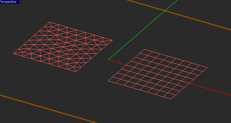
| − | It is well known that any planar geometry with any degree of complexity can be reasonably discretized using a surface triangular mesh. EM.Cube's [[Planar Module]] provides a versatile triangular mesh generator for this purpose. This generates a regular mesh, in which most of the triangular cells have almost equal areas. The uniformity or regularity of mesh is an important factor in warranting a stable numerical solution. A highly incongruous mesh may even produce completely erroneous results. EM.Cube's [[Planar Module]] also offers another mesh generator that creates a "Hubrid" planar mesh combining triangular and rectangular cells. Although triangular cells are more versatile than rectangular cells in adapting to arbitrary geometries, many practical planar structures contain a large number of rectangular parts like patch antennas, microstrip lines and components, etc. | + | It is well known that any planar geometry with any degree of complexity can be reasonably discretized using a surface triangular mesh. [[EM.Cube]]'s [[Planar Module]] provides a versatile triangular mesh generator for this purpose. This generates a regular mesh, in which most of the triangular cells have almost equal areas. The uniformity or regularity of mesh is an important factor in warranting a stable numerical solution. A highly incongruous mesh may even produce completely erroneous results. [[EM.Cube]]'s [[Planar Module]] also offers another mesh generator that creates a "Hubrid" planar mesh combining triangular and rectangular cells. Although triangular cells are more versatile than rectangular cells in adapting to arbitrary geometries, many practical planar structures contain a large number of rectangular parts like patch antennas, microstrip lines and components, etc. |
[[File:PMOM32.png|800px]] | [[File:PMOM32.png|800px]] | ||
| Line 347: | Line 347: | ||
# Verifying the mesh for integrity | # Verifying the mesh for integrity | ||
| − | EM. | + | [[EM.Cube]]’s [[Planar Module]] offers two mesh generation algorithms for discretizing planar structures: Hybrid and Triangular. The hybrid mesh consists of both rectangular and triangular cells. The hybrid mesh generator creates a kind of “object-centric” mesh that depends on the geometry of each object. It tries to discretize rectangular objects with rectangular cells as much as possible. In certain connection areas, a few triangular cells might be inserted to provide the mesh transition for current continuity. All the non-rectangular objects (circular, polygonal, etc.) are discretized using triangular cells. The triangular mesh generator, on the other hand, discretizes the planar objects with all triangular cells regardless of their shape. The only exceptions are feed lines that contain gap sources or lumped elements, which are always meshed with rectangular cells. |
| − | You can generate and view a planar mesh by clicking the '''Show Mesh''' [[File:mesh_tool.png]] button of the '''Simulate Toolbar''' or by selecting '''Menu > Simulate > Discretization > Show Mesh''' or using the keyboard shortcut '''Ctrl+M'''. When the mesh of the planar structure is displayed in EM. | + | You can generate and view a planar mesh by clicking the '''Show Mesh''' [[File:mesh_tool.png]] button of the '''Simulate Toolbar''' or by selecting '''Menu > Simulate > Discretization > Show Mesh''' or using the keyboard shortcut '''Ctrl+M'''. When the mesh of the planar structure is displayed in [[EM.Cube]]’s project workspace, its "Mesh View" mode is enabled. In this mode you can perform view operations like rotate view, pan or zoom, but you cannot create new objects or edit existing ones. To exit the mesh view mode, press the keyboard's '''Esc Key''' or click the '''Show Mesh''' [[File:mesh_tool.png]] button once again. |
| − | Once a mesh is generated, it stays in the memory until the structure is changed or the mesh density or other settings are modified. Every time you view mesh, the one in the memory is displayed. You can force EM.Cube to create a new mesh from the ground up by selecting '''Menu > Simulate > Discretization > Regenerate Mesh''' or by right clicking on the '''Planar Mesh''' item in the '''Discretization''' section of the Navigation Tree and selecting '''Regenerate''' from the contextual menu. | + | Once a mesh is generated, it stays in the memory until the structure is changed or the mesh density or other settings are modified. Every time you view mesh, the one in the memory is displayed. You can force [[EM.Cube]] to create a new mesh from the ground up by selecting '''Menu > Simulate > Discretization > Regenerate Mesh''' or by right clicking on the '''Planar Mesh''' item in the '''Discretization''' section of the Navigation Tree and selecting '''Regenerate''' from the contextual menu. |
=== Planar Mesh Density === | === Planar Mesh Density === | ||
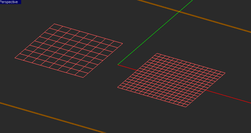
| − | EM.Cube's [[Planar Module]], by default, generates a hybrid mesh of your planar structure with a mesh density of 20 cells per effective wavelength. It is important to understand the concept of mesh density (either hybrid or triangular) as used by [[Planar Module]]. It gives a measure of the number of cells per effective wavelength that are placed in various regions of your planar structure. The higher the mesh density, the more cells are created on the geometrical objects. Keep in mind that only the finite-sized objects of your structure are discretized. No mesh is generated for the substrate layers of your background structure. The free-space wavelength is defined as <math>\lambda_0 = \tfrac{2\pi f}{c}</math>, where f is the center frequency of your project and c is the speed of light in the free space. The effective wavelength is defined as <math>\lambda_{eff} = \tfrac{\lambda_0}{\sqrt{\varepsilon_{eff}}}</math>, where e<sub>eff</sub> is the effective permittivity. | + | [[EM.Cube]]'s [[Planar Module]], by default, generates a hybrid mesh of your planar structure with a mesh density of 20 cells per effective wavelength. It is important to understand the concept of mesh density (either hybrid or triangular) as used by [[Planar Module]]. It gives a measure of the number of cells per effective wavelength that are placed in various regions of your planar structure. The higher the mesh density, the more cells are created on the geometrical objects. Keep in mind that only the finite-sized objects of your structure are discretized. No mesh is generated for the substrate layers of your background structure. The free-space wavelength is defined as <math>\lambda_0 = \tfrac{2\pi f}{c}</math>, where f is the center frequency of your project and c is the speed of light in the free space. The effective wavelength is defined as <math>\lambda_{eff} = \tfrac{\lambda_0}{\sqrt{\varepsilon_{eff}}}</math>, where e<sub>eff</sub> is the effective permittivity. |
| − | The effective permittivity is defined differently for different types of traces and embedded object sets. For metal and conductive sheet traces, the effective permittivity is defined as the larger of the permittivity of the two substrate layers just above and below the metallic trace. For slot traces, the effective permittivity is defined as the mean (average) of the permittivity of the two substrate layers just above and below the metallic trace. These definitions of effective permittivity are consistent with the effective propagation constant of transmission lines realized on such trace types. For embedded object sets, the effective permittivity is defined as the largest of the permittivities of all the substrate layers and embedded dielectric sets. In all cases, for the purpose of calculating the effective wavelength, only the real part of the permittivities are considered. The reason for using an effective wavelength so defined for determination of mesh resolution is to make sure that enough cells are placed in areas that might feature higher field concentration. | + | The effective permittivity is defined differently for different types of traces and embedded object sets. For metal and conductive sheet traces, the effective permittivity is defined as the larger of the permittivity of the two substrate layers just above and below the metallic trace. For slot traces, the effective permittivity is defined as the mean (average) of the permittivity of the two substrate layers just above and below the metallic trace. These definitions of effective permittivity are consistent with the effective propagation constant of [[Transmission Lines|transmission lines]] realized on such trace types. For embedded object sets, the effective permittivity is defined as the largest of the permittivities of all the substrate layers and embedded dielectric sets. In all cases, for the purpose of calculating the effective wavelength, only the real part of the permittivities are considered. The reason for using an effective wavelength so defined for determination of mesh resolution is to make sure that enough cells are placed in areas that might feature higher field concentration. |
Due to the different definitions of effective wavelength in different parts of your planar structure, you will see different mesh resolutions. For example, if you structure has several substrate layers with different permittivities, the mesh of metal traces on layers with a higher permittivity value will feature more cells than the mesh of metal traces on layers with a lower permittivity value even though the mesh density value is the same for the whole structure. | Due to the different definitions of effective wavelength in different parts of your planar structure, you will see different mesh resolutions. For example, if you structure has several substrate layers with different permittivities, the mesh of metal traces on layers with a higher permittivity value will feature more cells than the mesh of metal traces on layers with a lower permittivity value even though the mesh density value is the same for the whole structure. | ||
| Line 375: | Line 375: | ||
=== Mesh Of Connected Trace Objects === | === Mesh Of Connected Trace Objects === | ||
| − | Using the generated mesh of a planar structure, EM.Cube creates a set of vectorial basis functions that are passed to the input file of the Planar MoM simulation engine. This engine requires edge-based basis functions. The common edges between adjacent cells are used to define edge-based rooftop or RWG basis functions. These elementary basis functions indeed provide the current flow and warrant the continuity among the mesh cells. Therefore, when two objects overlap or share a common edge, the connection between them must be translated into "bridge" basis functions, which carry the information about current flow to the simulation engine. | + | Using the generated mesh of a planar structure, [[EM.Cube]] creates a set of vectorial basis functions that are passed to the input file of the Planar MoM simulation engine. This engine requires edge-based basis functions. The common edges between adjacent cells are used to define edge-based rooftop or RWG basis functions. These elementary basis functions indeed provide the current flow and warrant the continuity among the mesh cells. Therefore, when two objects overlap or share a common edge, the connection between them must be translated into "bridge" basis functions, which carry the information about current flow to the simulation engine. |
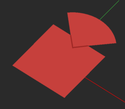
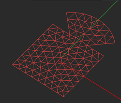
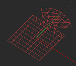
| − | '''The most important rule of object connections in EM.Cube's [[Planar Module]] is that only objects belonging to the same trace can be connected to one another.''' For example, if two objects reside on the same Z-plane and geometrically have a common edge which you can clearly see in the project workspace, but organizationally they belong to two different metal traces, then the bridge basis functions will not be generated between them, and the simulation engine will see them disconnected. If two objects belong to the same trace and have a common overlap area, EM.Cube first merges the two objects using the "Boolean Union" operation and converts them into a single object for the purpose of meshing. The mesh of "unioned" areas is usually made up of triangular cells. If two objects reside on the same Z-plane and geometrically overlap with each other but organizationally belong to two different trace groups, incongruous, overlapped cells will be generated that will either blow up the linear system or produce completely wrong simulation results. | + | '''The most important rule of object connections in [[EM.Cube]]'s [[Planar Module]] is that only objects belonging to the same trace can be connected to one another.''' For example, if two objects reside on the same Z-plane and geometrically have a common edge which you can clearly see in the project workspace, but organizationally they belong to two different metal traces, then the bridge basis functions will not be generated between them, and the simulation engine will see them disconnected. If two objects belong to the same trace and have a common overlap area, [[EM.Cube]] first merges the two objects using the "Boolean Union" operation and converts them into a single object for the purpose of meshing. The mesh of "unioned" areas is usually made up of triangular cells. If two objects reside on the same Z-plane and geometrically overlap with each other but organizationally belong to two different trace groups, incongruous, overlapped cells will be generated that will either blow up the linear system or produce completely wrong simulation results. |
[[File:PMOM36.png|250px]] [[File:PMOM38.png|250px]] [[File:PMOM37.png|250px]] | [[File:PMOM36.png|250px]] [[File:PMOM38.png|250px]] [[File:PMOM37.png|250px]] | ||
| Line 383: | Line 383: | ||
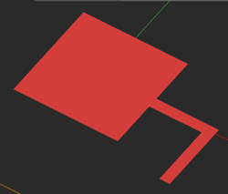
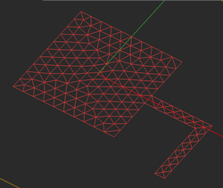
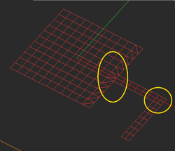
Figure 1: Two overlapping planar objects and their triangular and hybrid planar meshes. | Figure 1: Two overlapping planar objects and their triangular and hybrid planar meshes. | ||
| − | When two planar objects belonging to the same trace are connected via a common edge, it is critical to generate a consistent mesh at the connection area and properly transition and merge the meshes of the individual objects. EM.Cube's triangular planar mesh generator simply "unions" the two objects and generates a connected mesh. EM.Cube's hybrid planar mesh generator, however, behave differently when it comes to the connection between rectangular objects. The rule in this case is the following: | + | When two planar objects belonging to the same trace are connected via a common edge, it is critical to generate a consistent mesh at the connection area and properly transition and merge the meshes of the individual objects. [[EM.Cube]]'s triangular planar mesh generator simply "unions" the two objects and generates a connected mesh. [[EM.Cube]]'s hybrid planar mesh generator, however, behave differently when it comes to the connection between rectangular objects. The rule in this case is the following: |
* If the two connected rectangular objects have the same side dimensions along the common linear edge with perfect alignment, a rectangular bridge mesh is produced. | * If the two connected rectangular objects have the same side dimensions along the common linear edge with perfect alignment, a rectangular bridge mesh is produced. | ||
| Line 395: | Line 395: | ||
=== Mesh of Embedded Objects === | === Mesh of Embedded Objects === | ||
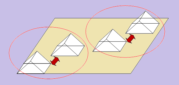
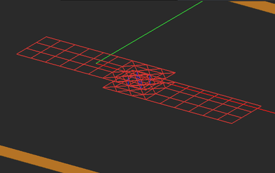
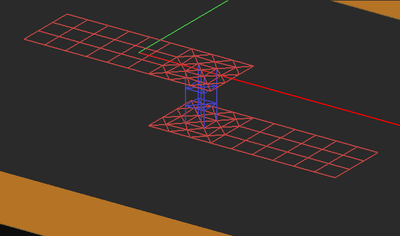
| − | EM.Cube's [[Planar Module]] models embedded objects as vertical volume currents. The vectorial basis functions in this case are Z-directed prisms as opposed to rooftop basis functions. If an embedded object is located under or above a metallic trace or connected from both top and bottom, it is critical to create mesh continuity between the embedded object and its connected metallic traces. In other words, the generated mesh must ensure current continuity between the vertical volume currents and horizontal surface currents. EM. | + | [[EM.Cube]]'s [[Planar Module]] models embedded objects as vertical volume currents. The vectorial basis functions in this case are Z-directed prisms as opposed to rooftop basis functions. If an embedded object is located under or above a metallic trace or connected from both top and bottom, it is critical to create mesh continuity between the embedded object and its connected metallic traces. In other words, the generated mesh must ensure current continuity between the vertical volume currents and horizontal surface currents. [[EM.Cube]]’s planar mesh generator automatically handles situations of this kind and generates all the required connection meshes. |
| − | Keep in mind that EM. | + | Keep in mind that [[EM.Cube]]’s Planar MoM engine uses a 2.5-D approximation, whereby only vertical volume currents are assumed inside embedded objects. When the height of an embedded object is small (as should typically be under the 2.5-D assumption), one prismatic cell is placed across the object along the Z-axis. Long PEC vias with a very small radius do also satisfy the 2.5-D assumption. In this case, the long via objects are discretized further along the Z direction and generate multiple stacked cells. Several prismatic cells along the Z-axis may increase the simulation time drastically. This is due to the fact that the host layer is effectively subdivided into a number of sub-layers and the stacked cells are treated as stacked vias embedded inside these sub-layers. As a result, the simulation engine needs to compute all the dyadic Green’s functions accounting for the interactions between all such sub-layers. |
[[File:PMOM39.png|400px]] [[File:PMOM40.png|400px]] | [[File:PMOM39.png|400px]] [[File:PMOM40.png|400px]] | ||
| Line 407: | Line 407: | ||
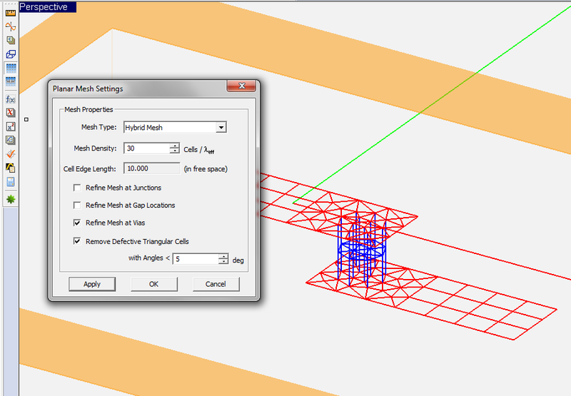
It is very important to apply the right mesh density to capture all the geometrical details of your planar structure. This is especially true for "field discontinuity" regions such as junction areas between objects of different side dimensions, where larger current concentrations are usually observed at sharp corners, or at the connection areas between metallic traces and PEC vias, as well as the areas around gap sources and lumped elements, as these create voltage or current discontinuities. For large planar structures, using a higher mesh density may not always be a practical option since it will quickly lead to a very large MoM matrix and thus growing the size of the numerical problem. Sometimes a slightly non-uniform mesh still produces stable numerical results. In other words, you may choose to increase the mesh resolution around the discontinuity regions only. | It is very important to apply the right mesh density to capture all the geometrical details of your planar structure. This is especially true for "field discontinuity" regions such as junction areas between objects of different side dimensions, where larger current concentrations are usually observed at sharp corners, or at the connection areas between metallic traces and PEC vias, as well as the areas around gap sources and lumped elements, as these create voltage or current discontinuities. For large planar structures, using a higher mesh density may not always be a practical option since it will quickly lead to a very large MoM matrix and thus growing the size of the numerical problem. Sometimes a slightly non-uniform mesh still produces stable numerical results. In other words, you may choose to increase the mesh resolution around the discontinuity regions only. | ||
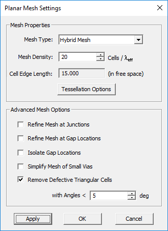
| − | The Planar Mesh Settings dialog gives a few more options for customizing your planar mesh around geometrical and field discontinuities. You can check the check box labeled "'''Refine Mesh at Junctions'''", which increases the mesh resolution at the connection area between rectangular objects. Or you can check the check box labeled "'''Refine Mesh at Gap Locations'''", which may prove particularly useful when gap sources or lumped elements are placed on a short transmission line connected from both ends. Or you can check the check box labeled "'''Refine Mesh at Vias'''", which increases the mesh resolution on the cross section of embedded object sets and by extension at the connection regions of the metallic objects connected to them. EM.Cube typically doubles the mesh resolution locally at the discontinuity areas when the respective boxes are checked. | + | The Planar Mesh Settings dialog gives a few more options for customizing your planar mesh around geometrical and field discontinuities. You can check the check box labeled "'''Refine Mesh at Junctions'''", which increases the mesh resolution at the connection area between rectangular objects. Or you can check the check box labeled "'''Refine Mesh at Gap Locations'''", which may prove particularly useful when gap sources or lumped elements are placed on a short transmission line connected from both ends. Or you can check the check box labeled "'''Refine Mesh at Vias'''", which increases the mesh resolution on the cross section of embedded object sets and by extension at the connection regions of the metallic objects connected to them. [[EM.Cube]] typically doubles the mesh resolution locally at the discontinuity areas when the respective boxes are checked. |
[[File:PMOM41.png|800px]] | [[File:PMOM41.png|800px]] | ||
| Line 415: | Line 415: | ||
=== Checking Mesh Integrity === | === Checking Mesh Integrity === | ||
| − | You should always visually inspect EM.Cube's default generated mesh to see if the current mesh settings have produced an acceptable mesh. You may often need to change the mesh density or other parameters and regenerate the mesh. The Planar Mesh Settings dialog gives a few more options for customizing your planar mesh. | + | You should always visually inspect [[EM.Cube]]'s default generated mesh to see if the current mesh settings have produced an acceptable mesh. You may often need to change the mesh density or other [[parameters]] and regenerate the mesh. The Planar Mesh Settings dialog gives a few more options for customizing your planar mesh. |
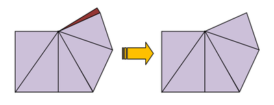
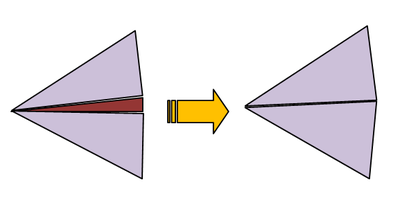
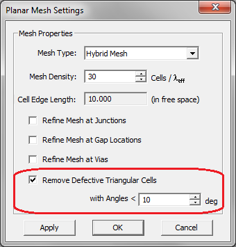
| − | As mentioned earlier, highly incongruous meshes should always be avoided. Sometimes EM.Cube's default mesh may contain very narrow triangular cells due to very small angles between two edges. In some rare cases, extremely small triangular cells may be generated, whose area is a small fraction of the average mesh cell. These cases typically happen at the junctions and other discontinuity regions or at the boundary of highly irregular geometries with extremely fine details. In such cases, increasing or decreasing the mesh density by one or few cells per effective wavelength often resolves that problem and eliminates those defective cells. Nonetheless, EM.Cube's planar mesh generator offers an option to identify the defective triangular cells and either delete them or cure them. By curing we mean removing a narrow triangular cell and merging its two closely spaced nodes to fill the crack left behind. | + | As mentioned earlier, highly incongruous meshes should always be avoided. Sometimes [[EM.Cube]]'s default mesh may contain very narrow triangular cells due to very small angles between two edges. In some rare cases, extremely small triangular cells may be generated, whose area is a small fraction of the average mesh cell. These cases typically happen at the junctions and other discontinuity regions or at the boundary of highly irregular geometries with extremely fine details. In such cases, increasing or decreasing the mesh density by one or few cells per effective wavelength often resolves that problem and eliminates those defective cells. Nonetheless, [[EM.Cube]]'s planar mesh generator offers an option to identify the defective triangular cells and either delete them or cure them. By curing we mean removing a narrow triangular cell and merging its two closely spaced nodes to fill the crack left behind. |
[[File:PMOM44.png|400px]] [[File:PMOM42.png|400px]] | [[File:PMOM44.png|400px]] [[File:PMOM42.png|400px]] | ||
| Line 423: | Line 423: | ||
Deleting or curing defective triangular cells. | Deleting or curing defective triangular cells. | ||
| − | EM.Cube by default deletes or cures all the triangular cells that have angles less than 10º. Sometimes removing defective cells may inadvertently cause worse problems in the mesh. You may choose to disable this feature and uncheck the box labeled "'''Remove Defective Triangular Cells'''" in the Planar Mesh Settings dialog. You can also change the value of the minimum allowable cell angle. | + | [[EM.Cube]] by default deletes or cures all the triangular cells that have angles less than 10º. Sometimes removing defective cells may inadvertently cause worse problems in the mesh. You may choose to disable this feature and uncheck the box labeled "'''Remove Defective Triangular Cells'''" in the Planar Mesh Settings dialog. You can also change the value of the minimum allowable cell angle. |
[[File:PMOM43(1).png]] | [[File:PMOM43(1).png]] | ||
| Line 431: | Line 431: | ||
=== Locking Mesh Of Object Groups === | === Locking Mesh Of Object Groups === | ||
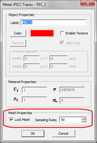
| − | EM.Cube's [[Planar Module]] provides different ways of controlling the mesh of a planar structure locally. Earlier you saw how to increase the mesh resolution at the discontinuity regions without affecting the mesh of uniform or regular areas of a planar structure. Another way of local mesh control is to lock the mesh density of certain traces or object sets. The mesh density that you specify in the Planar Mesh Settings dialog is a global parameter and applies to all the traces and embedded object sets in your project. However, you can lock the mesh of individual PEC, PMC and conductive sheet traces or embedded objects sets. In that case, the locked mesh density takes precedence over the global density. Note that locking mesh of object groups, in principle, is different than refining the mesh at discontinuities. In the latter case, the mesh of connection areas is affected. However, objects belonging to different traces cannot be connected to one another. Therefore, locking mesh can be useful primarily for isolated object groups that may require a higher (or lower) mesh resolution. | + | [[EM.Cube]]'s [[Planar Module]] provides different ways of controlling the mesh of a planar structure locally. Earlier you saw how to increase the mesh resolution at the discontinuity regions without affecting the mesh of uniform or regular areas of a planar structure. Another way of local mesh control is to lock the mesh density of certain traces or object sets. The mesh density that you specify in the Planar Mesh Settings dialog is a global parameter and applies to all the traces and embedded object sets in your project. However, you can lock the mesh of individual PEC, PMC and conductive sheet traces or embedded objects sets. In that case, the locked mesh density takes precedence over the global density. Note that locking mesh of object groups, in principle, is different than refining the mesh at discontinuities. In the latter case, the mesh of connection areas is affected. However, objects belonging to different traces cannot be connected to one another. Therefore, locking mesh can be useful primarily for isolated object groups that may require a higher (or lower) mesh resolution. |
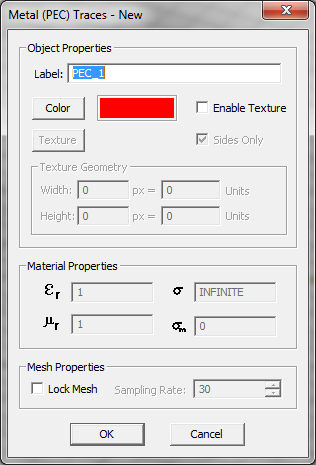
You can lock the local mesh density by accessing the property dialog of a specific trace or embedded object set and checking the box labeled '''Lock Mesh'''. This will enable the '''Mesh Density''' box, where you can accept the default global value or set any desired new value. | You can lock the local mesh density by accessing the property dialog of a specific trace or embedded object set and checking the box labeled '''Lock Mesh'''. This will enable the '''Mesh Density''' box, where you can accept the default global value or set any desired new value. | ||
| Line 441: | Line 441: | ||
=== Local Mesh Control Using Polymesh Objects === | === Local Mesh Control Using Polymesh Objects === | ||
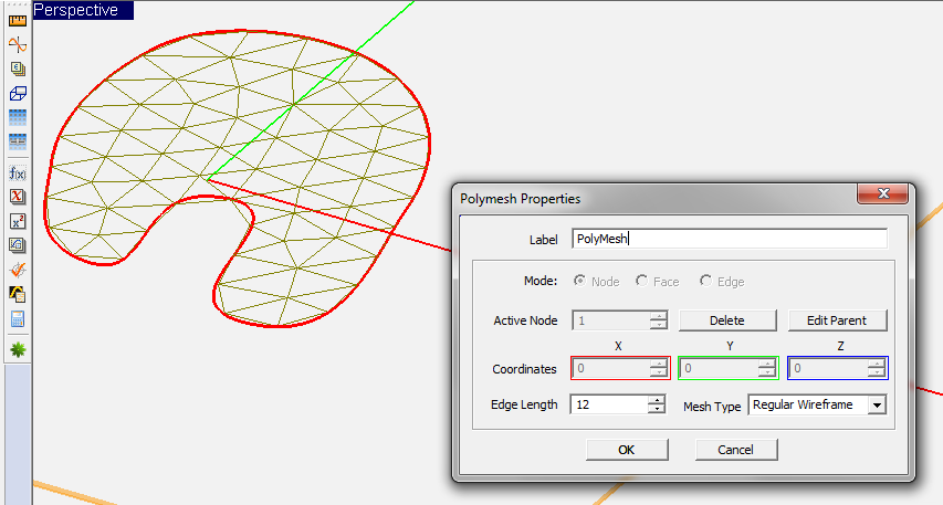
| − | EM.Cube allows you to manually and individually mesh geometrical objects using the concept of polymesh. The Polymesh tool converts a planar surface object to a set of interconnected triangular cells, which is basically identical to its triangular surface mesh. Simply select an object and click the '''Polymesh Tool''' [[File:polymesh_tool_tn.png]] button of '''Tools Toolbar''', or select '''Menu > Tools > Polymesh''', or use the keyboard shortcut '''P'''. You can also right click on a selected object and select '''Polymesh''' from the contextual menu. From the Polymesh Dialog, you can control the mesh resolution through the '''Edge Length''' parameter, which is expressed in project units. Note that unlike the planar mesh generator which uses a frequency-dependent mesh density to drive the mesh resolution, the ploymesh's edge length is fixed and purely geometrical and does not change with the project frequency. '''EM.Cube's mesh generator considers a polymesh object as a "final" mesh and reproduces it "As Is" during the meshing process.''' | + | [[EM.Cube]] allows you to manually and individually mesh geometrical objects using the concept of polymesh. The Polymesh tool converts a planar surface object to a set of interconnected triangular cells, which is basically identical to its triangular surface mesh. Simply select an object and click the '''Polymesh Tool''' [[File:polymesh_tool_tn.png]] button of '''Tools Toolbar''', or select '''Menu > Tools > Polymesh''', or use the keyboard shortcut '''P'''. You can also right click on a selected object and select '''Polymesh''' from the contextual menu. From the Polymesh Dialog, you can control the mesh resolution through the '''Edge Length''' parameter, which is expressed in project units. Note that unlike the planar mesh generator which uses a frequency-dependent mesh density to drive the mesh resolution, the ploymesh's edge length is fixed and purely geometrical and does not change with the project frequency. '''[[EM.Cube]]'s mesh generator considers a polymesh object as a "final" mesh and reproduces it "As Is" during the meshing process.''' |
You have access to every single node of a polymesh object and you can change its coordinates arbitrarily. You do this by opening the property dialog of a polymesh object and selecting a certain node index in the box labeled '''Active Node'''. You can also select a node by hovering the mouse over the node to highlight it and then click to select it. A red ball appears on the current active node. You can delete the nodes arbitrarily using the '''Delete''' button of the dialog, which results in lowering the mesh resolution at the location of the deleted node. Or you can insert new nodes in the faces of a polymesh object. To insert a node, first you have to select a face. Change the '''Mode''' option by selecting the '''Face''' radio button and then select the right '''Active Face''' index. A red triangular border appears around the selected face. You can also simply click on the surface of a face and select it using the mouse. With the desired face selected, click the '''Insert''' button of the dialog to create a new node at the centroid of the selected face. You can adjust the coordinates of the newly inserted node from the three X, Y and Z '''Coordinate''' boxes. Note that immediately after the insertion of a new node, the label of these coordinate boxes changes to "'''New Node'''" and they show the relative local X, Y and Z offsets with respect to the original node position. Once you close the Polymesh Dialog, the new node is added to the existing node list and can be edited later like the other polymesh nodes. By inserting a new node, you increase the mesh resolution locally and selectively. | You have access to every single node of a polymesh object and you can change its coordinates arbitrarily. You do this by opening the property dialog of a polymesh object and selecting a certain node index in the box labeled '''Active Node'''. You can also select a node by hovering the mouse over the node to highlight it and then click to select it. A red ball appears on the current active node. You can delete the nodes arbitrarily using the '''Delete''' button of the dialog, which results in lowering the mesh resolution at the location of the deleted node. Or you can insert new nodes in the faces of a polymesh object. To insert a node, first you have to select a face. Change the '''Mode''' option by selecting the '''Face''' radio button and then select the right '''Active Face''' index. A red triangular border appears around the selected face. You can also simply click on the surface of a face and select it using the mouse. With the desired face selected, click the '''Insert''' button of the dialog to create a new node at the centroid of the selected face. You can adjust the coordinates of the newly inserted node from the three X, Y and Z '''Coordinate''' boxes. Note that immediately after the insertion of a new node, the label of these coordinate boxes changes to "'''New Node'''" and they show the relative local X, Y and Z offsets with respect to the original node position. Once you close the Polymesh Dialog, the new node is added to the existing node list and can be edited later like the other polymesh nodes. By inserting a new node, you increase the mesh resolution locally and selectively. | ||
| Line 447: | Line 447: | ||
[[File:PMOM46(1).png]] | [[File:PMOM46(1).png]] | ||
| − | Figure 2: Discretizing a planar surface object using EM.Cube's Polymesh tool. | + | Figure 2: Discretizing a planar surface object using [[EM.Cube]]'s Polymesh tool. |
| − | Keep in mind that since a polymesh object it considered a final mesh, its mesh cannot be connected to other objects. In other words, bridge basis functions are not generated if even some of the polymesh edges may coincide with other objects' edges. A polymesh object is treated by the mesh generator as an isolated mesh. However, EM.Cube allows you to connect polymesh objects manually. To do so, bring two or more polymesh objects close to each other so that they have one or more common edges. No face overlaps are allowed in this case. Select the polymesh objects and click the '''Merge Tool'''[[File:merge_tool_tn.png]] button of '''Tools Toolbar''' to merge the polymesh objects into a single polymesh object. The new merged polymesh object will provide all the necessary bridge basis functions among the original, separate polymesh objects. | + | Keep in mind that since a polymesh object it considered a final mesh, its mesh cannot be connected to other objects. In other words, bridge basis functions are not generated if even some of the polymesh edges may coincide with other objects' edges. A polymesh object is treated by the mesh generator as an isolated mesh. However, [[EM.Cube]] allows you to connect polymesh objects manually. To do so, bring two or more polymesh objects close to each other so that they have one or more common edges. No face overlaps are allowed in this case. Select the polymesh objects and click the '''Merge Tool'''[[File:merge_tool_tn.png]] button of '''Tools Toolbar''' to merge the polymesh objects into a single polymesh object. The new merged polymesh object will provide all the necessary bridge basis functions among the original, separate polymesh objects. |
== Excitation Sources == | == Excitation Sources == | ||
| − | In a typical electromagnetic simulation in EM.Cube's [[Planar Module]], you define a planar structure that consists of a layered background structure with a number of finite-sized metal and slot traces and possibly embedded metal or dielectric objects interspersed among the substrate layers. The planar structure is then excited by some sort of a signal source that induces electric currents on metal parts and magnetic currents on slot traces. The method of moments (MoM) solver computes these unknown electric and magnetic currents by discretizing the finite-sized objects. The induced currents, in turn, produce their own electric and magnetic fields which coexist (are superposed) with the impressed electric and magnetic fields of the signal source. From a knowledge of the near fields, EM.Cube calculates the port characteristics of the planar structure, if any ports have been defined. From a knowledge of the far fields, EM.Cube calculates the radiation or scattering characteristics of the planar structure. | + | In a typical electromagnetic simulation in [[EM.Cube]]'s [[Planar Module]], you define a planar structure that consists of a layered background structure with a number of finite-sized metal and slot traces and possibly embedded metal or dielectric objects interspersed among the substrate layers. The planar structure is then excited by some sort of a signal source that induces electric currents on metal parts and magnetic currents on slot traces. The method of moments (MoM) solver computes these unknown electric and magnetic currents by discretizing the finite-sized objects. The induced currents, in turn, produce their own electric and magnetic fields which coexist (are superposed) with the impressed electric and magnetic fields of the signal source. From a knowledge of the near fields, [[EM.Cube]] calculates the port characteristics of the planar structure, if any ports have been defined. From a knowledge of the far fields, [[EM.Cube]] calculates the radiation or scattering characteristics of the planar structure. |
You can excite a planar structure in a number of different ways. The excitation source you choose depends on the observables you seek in your project. [[Planar Module]] provides the following source for exciting planar structures: | You can excite a planar structure in a number of different ways. The excitation source you choose depends on the observables you seek in your project. [[Planar Module]] provides the following source for exciting planar structures: | ||
| Line 462: | Line 462: | ||
* [[#Huygens Sources|Huygens Sources]] | * [[#Huygens Sources|Huygens Sources]] | ||
| − | For antennas and planar circuits, where you typically define one or more ports, you usually use lumped sources. A lumped source is indeed a gap discontinuity that is placed on the path of an electric or magnetic current flow, where a voltage or current source is connected to inject a signal. Gap sources are placed across metal or slot traces. Probe sources are placed across vertical PEC vias. A de-embedded source is a special type of gap source that is placed near the open end of an elongated metal or slot trace to create a standing wave pattern, from which the scattering parameters can be calculated accurately. To calculate the scattering characteristics of a planar structure, e.g. its radar cross section (RCS), you excite it with a plane wave source. Short dipole sources are used to explore propagation of points sources along a layered structure. Huygens sources are virtual equivalent sources that capture the radiated electric and magnetic fields from another structure possibly in another EM.Cube computational module and bring them as a new source to excite your planar structure. | + | For antennas and planar circuits, where you typically define one or more ports, you usually use lumped sources. A lumped source is indeed a gap discontinuity that is placed on the path of an electric or magnetic current flow, where a voltage or current source is connected to inject a signal. Gap sources are placed across metal or slot traces. Probe sources are placed across vertical PEC vias. A de-embedded source is a special type of gap source that is placed near the open end of an elongated metal or slot trace to create a standing wave pattern, from which the scattering [[parameters]] can be calculated accurately. To calculate the scattering characteristics of a planar structure, e.g. its radar cross section (RCS), you excite it with a plane wave source. Short dipole sources are used to explore propagation of points sources along a layered structure. Huygens sources are virtual equivalent sources that capture the radiated electric and magnetic fields from another structure possibly in another [[EM.Cube]] computational module and bring them as a new source to excite your planar structure. |
=== Gap Sources === | === Gap Sources === | ||
| Line 486: | Line 486: | ||
[[File:PMOM48.png|thumb|250px|The [[Planar Module]]'s Probe Source dialog]] | [[File:PMOM48.png|thumb|250px|The [[Planar Module]]'s Probe Source dialog]] | ||
| − | Another way of exciting a planar structure is by placing a gap on the path of a vertical current on a PEC via. This represents a filament source, which is used to model coaxial probe excitation. A probe source can be placed only on a PEC via object. Most planar transmission lines are fed using SMA connectors. The outer conductor of the coaxial line is connected to the ground and its inner conductor is extended across the substrate layer and connected to a metallic line. EM.Cube's [[Planar Module]] models a coaxial probe as an infinitesimal gap discontinuity placed across a thin via, representing an ideal voltage source in series with a lumped impedance. When the impedance is zero, the gap acts like an ideal lumped source and creates a uniform electric field across the via. The source pumps vertical electric current into the probe. If the voltage source is shorted (having a zero amplitude), then the gap acts like a shunt lumped element across the via. | + | Another way of exciting a planar structure is by placing a gap on the path of a vertical current on a PEC via. This represents a filament source, which is used to model coaxial probe excitation. A probe source can be placed only on a PEC via object. Most planar [[Transmission Lines|transmission lines]] are fed using SMA connectors. The outer conductor of the coaxial line is connected to the ground and its inner conductor is extended across the substrate layer and connected to a metallic line. [[EM.Cube]]'s [[Planar Module]] models a coaxial probe as an infinitesimal gap discontinuity placed across a thin via, representing an ideal voltage source in series with a lumped impedance. When the impedance is zero, the gap acts like an ideal lumped source and creates a uniform electric field across the via. The source pumps vertical electric current into the probe. If the voltage source is shorted (having a zero amplitude), then the gap acts like a shunt lumped element across the via. |
To define a probe source, follow these steps: | To define a probe source, follow these steps: | ||
| Line 507: | Line 507: | ||
Figure 1: Defining gap sources on an array of rectangle strip objects with a Chebyshev amplitude distribution. | Figure 1: Defining gap sources on an array of rectangle strip objects with a Chebyshev amplitude distribution. | ||
| − | In the data file option, the complex amplitude are directly read in from a data file using a real - imaginary format. When this option is selected, you can either improvise the complex array weights or import them from an existing file. In the former case click the '''New Data File''' button. This opens up the Windows Notepad with default formatted data file that has a list of all the array element indices with default 1+j0 amplitudes for all of them. You can replace the default complex values with new one and save the Notepad data file, which brings you back to the Gap Source dialog. To import the array weights, click the '''Open Data File''' button, which opens the standard Windows Open dialog. You can then select the right data file from the one of your folders. It is important to note that the data file must have the correct format to be read by EM.Cube. For this reason, it is recommended that you first create a new data file with the right format using Notepad as described earlier and then save it for later use. | + | In the data file option, the complex amplitude are directly read in from a data file using a real - imaginary format. When this option is selected, you can either improvise the complex array weights or import them from an existing file. In the former case click the '''New Data File''' button. This opens up the [[Windows]] Notepad with default formatted data file that has a list of all the array element indices with default 1+j0 amplitudes for all of them. You can replace the default complex values with new one and save the Notepad data file, which brings you back to the Gap Source dialog. To import the array weights, click the '''Open Data File''' button, which opens the standard [[Windows]] Open dialog. You can then select the right data file from the one of your folders. It is important to note that the data file must have the correct format to be read by [[EM.Cube]]. For this reason, it is recommended that you first create a new data file with the right format using Notepad as described earlier and then save it for later use. |
[[File:PMOM50.png|800px]] | [[File:PMOM50.png|800px]] | ||
| Line 515: | Line 515: | ||
=== Defining Ports === | === Defining Ports === | ||
| − | Ports are used in a planar structure to order and index the sources for calculation of circuit parameters such as scattering (S), impedance (Z) and admittance (Y) parameters. In EM.Cube's [[Planar Module]], you can use the following types of sources to define ports: | + | Ports are used in a planar structure to order and index the sources for calculation of circuit [[parameters]] such as scattering (S), impedance (Z) and admittance (Y) [[parameters]]. In [[EM.Cube]]'s [[Planar Module]], you can use the following types of sources to define ports: |
* Gap Sources | * Gap Sources | ||
| Line 540: | Line 540: | ||
You couple two or more sources using the '''Port Definition Dialog'''. To do so, you need to change the default port assignments. First, delete all the ports that are to be coupled from the Port List of the dialog. Then, define a new port by clicking the '''Add''' button of the dialog. This opens up the Add Port dialog, which consists of two tables: '''Available''' sources on the left and '''Associated''' sources on the right. A right arrow ('''-->''') button and a left arrow ('''<--''') button let you move the sources freely between these two tables. You will see in the "Available" table a list of all the sources that you deleted earlier. You may even see more available sources. Select all the sources that you want to couple and move them to the "Associated" table on the right. You can make multiple selections using the keyboard's '''Shift''' and '''Ctrl''' keys. Closing the Add Port dialog returns you to the Port Definition dialog, where you will now see the names of all the coupled sources next to the name of the newly added port. | You couple two or more sources using the '''Port Definition Dialog'''. To do so, you need to change the default port assignments. First, delete all the ports that are to be coupled from the Port List of the dialog. Then, define a new port by clicking the '''Add''' button of the dialog. This opens up the Add Port dialog, which consists of two tables: '''Available''' sources on the left and '''Associated''' sources on the right. A right arrow ('''-->''') button and a left arrow ('''<--''') button let you move the sources freely between these two tables. You will see in the "Available" table a list of all the sources that you deleted earlier. You may even see more available sources. Select all the sources that you want to couple and move them to the "Associated" table on the right. You can make multiple selections using the keyboard's '''Shift''' and '''Ctrl''' keys. Closing the Add Port dialog returns you to the Port Definition dialog, where you will now see the names of all the coupled sources next to the name of the newly added port. | ||
| − | {{Note|It is your responsibility to set up coupled ports and coupled transmission lines properly. For example, to excite the desirable odd mode of a coplanar waveguide (CPW), you need to create two rectangular slots parallel to and aligned with each other and place two gap sources on them with the same offsets and opposite polarities. To excite the even mode of the CPW, you use the same polarity for the two collocated gap sources. Whether you define a coupled port for the CPW or not, the right definition of sources will excite the proper mode. The couple ports are needed only for correct calculation of the port characteristics.}} | + | {{Note|It is your responsibility to set up coupled ports and coupled [[Transmission Lines|transmission lines]] properly. For example, to excite the desirable odd mode of a coplanar waveguide (CPW), you need to create two rectangular slots parallel to and aligned with each other and place two gap sources on them with the same offsets and opposite polarities. To excite the even mode of the CPW, you use the same polarity for the two collocated gap sources. Whether you define a coupled port for the CPW or not, the right definition of sources will excite the proper mode. The couple ports are needed only for correct calculation of the port characteristics.}} |
[[File:PMOM51(2).png|800px]] | [[File:PMOM51(2).png|800px]] | ||
| Line 589: | Line 589: | ||
=== Exciting Multiport Structures Using Linear Superposition === | === Exciting Multiport Structures Using Linear Superposition === | ||
| − | If your planar structure has two or more sources, but you have not defined any ports, all the lumped sources excite the structure locally and contribute to the excitation vector needed for the MoM solution of the problem. However, when you assign N ports to the sources, then you have a multiport structure that is characterized by an N×N admittance matrix (instead of a single Y<sub>in</sub> parameter), or an N×N impedance matrix, or an N×N scattering matrix. To calculate these matrices, EM.Cube uses a binary excitation scheme in conjunction with the principle of linear superposition. In this binary scheme, the structure is analyzed N times. Each time one of the N port-assigned sources is excited, and all the other port-assigned sources are turned off. | + | If your planar structure has two or more sources, but you have not defined any ports, all the lumped sources excite the structure locally and contribute to the excitation vector needed for the MoM solution of the problem. However, when you assign N ports to the sources, then you have a multiport structure that is characterized by an N×N admittance matrix (instead of a single Y<sub>in</sub> parameter), or an N×N impedance matrix, or an N×N scattering matrix. To calculate these matrices, [[EM.Cube]] uses a binary excitation scheme in conjunction with the principle of linear superposition. In this binary scheme, the structure is analyzed N times. Each time one of the N port-assigned sources is excited, and all the other port-assigned sources are turned off. |
| − | In the case of gap sources on metal traces and probe sources on PEC vias, turning a source off means shorting a series voltage source. The electric currents passing through these sources are then found at each port location, and the admittance parameters are found as follows: | + | In the case of gap sources on metal traces and probe sources on PEC vias, turning a source off means shorting a series voltage source. The electric currents passing through these sources are then found at each port location, and the admittance [[parameters]] are found as follows: |
:<math> I_m = \sum_{n=1}^N Y_{mn} V_n, \quad \quad Y_{mn} = \frac{I_m}{V_n} \bigg|_{V_k=0, k \ne n}</math> | :<math> I_m = \sum_{n=1}^N Y_{mn} V_n, \quad \quad Y_{mn} = \frac{I_m}{V_n} \bigg|_{V_k=0, k \ne n}</math> | ||
<!--[[File:PMOM57.png]]--> | <!--[[File:PMOM57.png]]--> | ||
| − | In the case of gap sources on slot traces, turning a source off means opening a shunt filament current source. The magnetic currents passing through the source locations, and thus the voltages across them, are then found at all ports, and the impedance parameters are found as follows: | + | In the case of gap sources on slot traces, turning a source off means opening a shunt filament current source. The magnetic currents passing through the source locations, and thus the voltages across them, are then found at all ports, and the impedance [[parameters]] are found as follows: |
:<math> V_m = \sum_{n=1}^N Z_{mn} I_n, \quad \quad Z_{mn} = \frac{V_m}{I_n} \bigg|_{I_k=0, k \ne n}</math> | :<math> V_m = \sum_{n=1}^N Z_{mn} I_n, \quad \quad Z_{mn} = \frac{V_m}{I_n} \bigg|_{I_k=0, k \ne n}</math> | ||
<!--[[File:PMOM58.png]]--> | <!--[[File:PMOM58.png]]--> | ||
| − | The N solution vectors that are generated through the N binary excitation analyses are finally superposed to produce the actual solution to the problem. However, in this process, EM.Cube also calculates all the port characteristics. Keep in mind that the impedance (Z) and admittance (Y) matrices are inverse of each other. From the impedance matrix, the scattering matrix is calculated using the following relation: | + | The N solution vectors that are generated through the N binary excitation analyses are finally superposed to produce the actual solution to the problem. However, in this process, [[EM.Cube]] also calculates all the port characteristics. Keep in mind that the impedance (Z) and admittance (Y) matrices are inverse of each other. From the impedance matrix, the scattering matrix is calculated using the following relation: |
:<math> \mathbf{[S] = [Y_0] \cdot ([Z]-[Z_0]) \cdot ([Z]+[Z_0])^{-1} \cdot [Z_0]} </math> | :<math> \mathbf{[S] = [Y_0] \cdot ([Z]-[Z_0]) \cdot ([Z]+[Z_0])^{-1} \cdot [Z_0]} </math> | ||
| Line 610: | Line 610: | ||
=== Modeling Lumped Elements In Planar MoM === | === Modeling Lumped Elements In Planar MoM === | ||
| − | Lumped elements are components, devices, or circuits whose overall dimensions are very small compared to the wavelength. As a result, they are considered to be dimensionless compared to the dimensions of a mesh cell. In fact, a lumped element is equivalent to an infinitesimally narrow gap that is placed in the path of current flow, across which the device's governing equations are enforced. Using Kirkhoff's laws, these device equations normally establish a relationship between the currents and voltages across the device or circuit. Crossing the bridge to Maxwell's domain, the device equations must now be cast into a from o boundary conditions that relate the electric and magnetic currents and fields. EM.Cube's [[Planar Module]] allows you to define passive circuit elements: '''Resistors'''(R), C'''apacitors'''(C), I'''nductors'''(L), and series and parallel combinations of them as shown in the figure below: | + | Lumped elements are components, devices, or circuits whose overall dimensions are very small compared to the wavelength. As a result, they are considered to be dimensionless compared to the dimensions of a mesh cell. In fact, a lumped element is equivalent to an infinitesimally narrow gap that is placed in the path of current flow, across which the device's governing equations are enforced. Using Kirkhoff's laws, these device equations normally establish a relationship between the currents and voltages across the device or circuit. Crossing the bridge to Maxwell's domain, the device equations must now be cast into a from o boundary conditions that relate the electric and magnetic currents and fields. [[EM.Cube]]'s [[Planar Module]] allows you to define passive circuit elements: '''Resistors'''(R), C'''apacitors'''(C), I'''nductors'''(L), and series and parallel combinations of them as shown in the figure below: |
[[File:image106.png]] | [[File:image106.png]] | ||
| Line 655: | Line 655: | ||
* In the '''Load Properties''' section, the series and shunt resistance values Rs and Rp are specified in Ohms, the series and shunt inductance values Ls and Lp are specified in nH (nanohenry), and the series and shunt capacitance values Cs and Cp are specified in pF (picofarad). Only the checked elements are taken into account in the total impedance calculation. By default, only the series resistor is checked with a value of 50S, and all other circuit elements are initially greyed out.<br /> | * In the '''Load Properties''' section, the series and shunt resistance values Rs and Rp are specified in Ohms, the series and shunt inductance values Ls and Lp are specified in nH (nanohenry), and the series and shunt capacitance values Cs and Cp are specified in pF (picofarad). Only the checked elements are taken into account in the total impedance calculation. By default, only the series resistor is checked with a value of 50S, and all other circuit elements are initially greyed out.<br /> | ||
| − | EM.Cube's [[Planar Module]] allows you to define a voltage source in series with a series-parallel RLC combination and place them across the gap. This is called an active lumped element. If you choose the '''Active with Gap Source''' option of the '''Lumped Circuit Type''' section of the dialog, the right section of the dialog entitled '''Source Properties''' becomes enabled, where you can you can specify the '''Source Amplitude''' in Volts (or in Amperes in the case of PMC traces) and the '''Phase''' in degrees. Also, the box labeled '''Direction''' becomes relevant in this case which contains a gap source. Otherwise, a passive RLC circuit does not have polarity. | + | [[EM.Cube]]'s [[Planar Module]] allows you to define a voltage source in series with a series-parallel RLC combination and place them across the gap. This is called an active lumped element. If you choose the '''Active with Gap Source''' option of the '''Lumped Circuit Type''' section of the dialog, the right section of the dialog entitled '''Source Properties''' becomes enabled, where you can you can specify the '''Source Amplitude''' in Volts (or in Amperes in the case of PMC traces) and the '''Phase''' in degrees. Also, the box labeled '''Direction''' becomes relevant in this case which contains a gap source. Otherwise, a passive RLC circuit does not have polarity. |
If the project workspace contains an array of rectangle strip objects or PEC via objects, the array object will also be listed as an eligible object for lumped element placement. A lumped element will then be placed on each element of the array. All the lumped elements will have identical direction, offset, resistance, inductance and capacitance values. If you define an active lumped element, you can prescribe certain amplitude and/or phase distribution to the gap sources just like in the case of gap and probe sources. The available amplitude distributions include '''Uniform''', '''Binomial'''''', Chebyshev''' and '''Data File'''. | If the project workspace contains an array of rectangle strip objects or PEC via objects, the array object will also be listed as an eligible object for lumped element placement. A lumped element will then be placed on each element of the array. All the lumped elements will have identical direction, offset, resistance, inductance and capacitance values. If you define an active lumped element, you can prescribe certain amplitude and/or phase distribution to the gap sources just like in the case of gap and probe sources. The available amplitude distributions include '''Uniform''', '''Binomial'''''', Chebyshev''' and '''Data File'''. | ||
| Line 663: | Line 663: | ||
=== Calculating Scattering Parameters Using Prony's Method === | === Calculating Scattering Parameters Using Prony's Method === | ||
| − | The calculation of the scattering (S) parameters is usually an important objective of modeling planar structures especially for planar circuits like filters, couplers, etc. As you saw earlier, you can use lumped sources like gaps and probes and even active lumped elements to calculate the circuit characteristics of planar structures. The admittance / impedance calculations based on the gap voltages and currents are accurate at RF and lower microwave frequencies or when the port transmission lines are narrow. In such cases, the electric or magnetic current distributions across the width of the port line are usually smooth, and quite uniform current or voltage profiles can easily be realized. At higher frequencies, however, a more robust method is needed for calculating the port parameters. | + | The calculation of the scattering (S) [[parameters]] is usually an important objective of modeling planar structures especially for planar circuits like filters, couplers, etc. As you saw earlier, you can use lumped sources like gaps and probes and even active lumped elements to calculate the circuit characteristics of planar structures. The admittance / impedance calculations based on the gap voltages and currents are accurate at RF and lower microwave frequencies or when the port [[Transmission Lines|transmission lines]] are narrow. In such cases, the electric or magnetic current distributions across the width of the port line are usually smooth, and quite uniform current or voltage profiles can easily be realized. At higher frequencies, however, a more robust method is needed for calculating the port [[parameters]]. |
| − | One can calculate the scattering parameters of a planar structure directly by analyzing the current distribution patterns on the port transmission lines. The discontinuity at the end of a port line typically gives rise to a standing wave pattern that can clearly be discerned in the line's current distribution. From the location of the current minima and maxima and their relative levels, one can determine the reflection coefficient at the discontinuity, i.e. the S<sub>11</sub> parameter. A more robust technique is Prony’s method, which is used for exponential approximation of functions. A complex function f(x) can be expanded as a sum of complex exponentials in the following form: | + | One can calculate the scattering [[parameters]] of a planar structure directly by analyzing the current distribution patterns on the port [[Transmission Lines|transmission lines]]. The discontinuity at the end of a port line typically gives rise to a standing wave pattern that can clearly be discerned in the line's current distribution. From the location of the current minima and maxima and their relative levels, one can determine the reflection coefficient at the discontinuity, i.e. the S<sub>11</sub> parameter. A more robust technique is Prony’s method, which is used for exponential approximation of functions. A complex function f(x) can be expanded as a sum of complex exponentials in the following form: |
:<math> f(x) \approx \sum_{n=1}^N c_i e^{-j\gamma_i x} </math> | :<math> f(x) \approx \sum_{n=1}^N c_i e^{-j\gamma_i x} </math> | ||
<!--[[File:PMOM73.png]]--> | <!--[[File:PMOM73.png]]--> | ||
| − | where c<sub>i</sub> are complex coefficients and γ<sub>i</sub> are, in general, complex exponents. From the physics of transmission lines, we know that lossless lines may support one or more propagating modes with pure real propagation constants (real γ<sub>i</sub> exponents). Moreover, line discontinuities generate evanescent modes with pure imaginary propagation constants (imaginary γ<sub>i</sub> exponents) that decay along the line as you move away from the location of such discontinuities. | + | where c<sub>i</sub> are complex coefficients and γ<sub>i</sub> are, in general, complex exponents. From the physics of [[Transmission Lines|transmission lines]], we know that lossless lines may support one or more propagating modes with pure real propagation constants (real γ<sub>i</sub> exponents). Moreover, line discontinuities generate evanescent modes with pure imaginary propagation constants (imaginary γ<sub>i</sub> exponents) that decay along the line as you move away from the location of such discontinuities. |
| − | In practical planar structures for which you want to calculate the scattering parameters, each port line normally supports one, and only one, dominant propagating mode. Multi-mode transmission lines are seldom used for practical RF and microwave applications. Nonetheless, each port line carries a superposition of incident and reflected dominant-mode propagating signals. An incident signal, by convention, is one that propagates along the line towards the discontinuity, where the phase reference plane is usually established. A reflected signal is one that propagates away from the port plane. Prony's method can be used to extract the incident and reflected propagating and evanescent exponential waves from the standing wave data. From a knowledge of the amplitudes (expansion coefficients) of the incident and reflected dominant propagating modes at all ports, the scattering matrix of the multi-port structure is then calculated. In Prony's method, the quality of the S parameter extraction results depends on the quality of the current samples and whether the port lines exhibit a dominant single-mode behavior. Clean current samples can be drawn in a region far from sources or discontinuities, typically a quarter wavelength away from the two ends of a feed line. | + | In practical planar structures for which you want to calculate the scattering [[parameters]], each port line normally supports one, and only one, dominant propagating mode. Multi-mode [[Transmission Lines|transmission lines]] are seldom used for practical RF and microwave applications. Nonetheless, each port line carries a superposition of incident and reflected dominant-mode propagating signals. An incident signal, by convention, is one that propagates along the line towards the discontinuity, where the phase reference plane is usually established. A reflected signal is one that propagates away from the port plane. Prony's method can be used to extract the incident and reflected propagating and evanescent exponential waves from the standing wave data. From a knowledge of the amplitudes (expansion coefficients) of the incident and reflected dominant propagating modes at all ports, the scattering matrix of the multi-port structure is then calculated. In Prony's method, the quality of the S parameter extraction results depends on the quality of the current samples and whether the port lines exhibit a dominant single-mode behavior. Clean current samples can be drawn in a region far from sources or discontinuities, typically a quarter wavelength away from the two ends of a feed line. |
[[File:PMOM71.png|800px]] | [[File:PMOM71.png|800px]] | ||
| Line 681: | Line 681: | ||
[[File:PMOM74.png|thumb|300px|The [[Planar Module]]'s De-embedded Source dialog]] | [[File:PMOM74.png|thumb|300px|The [[Planar Module]]'s De-embedded Source dialog]] | ||
| − | EM.Cube's [[Planar Module]] provides de-embedded sources for the exclusive purpose of accurate S parameter calculation based on Prony's method. A de-embedded source is indeed a gap source that is placed close to an open end of a feed line. The other end of the line is typically connected to a planar structure of interest. Like gap sources, de-embedded sources can be placed only on rectangle strip objects. '''During mesh generation, EM.Cube automatically extends the length of a port line that hosts a de-embedded source to about two effective wavelengths.''' This is done to provide enough length for formation of a clean standing wave current pattern. The effective wavelength of a transmission line for length extension purposes is calculated in a similar manner as for the planar mesh resolution. It is defined as <math>\lambda_{eff} = \tfrac{\lambda_0}{\sqrt{\varepsilon_{eff}}}</math>, where ε<sub>eff</sub> is the effective permittivity. For metal and conductive sheet traces, the effective permittivity is defined as the larger of the permittivities of the two substrate layers just above and below the metallic trace. For slot traces, the effective permittivity is defined as the mean (average) of the permittivities of the two substrate layers just above and below the metallic trace. The host port line must always be open from one end to allow for its length extension. You have to make sure that there are no objects standing on the way of the extended port line to avoid any unwanted overlaps. | + | [[EM.Cube]]'s [[Planar Module]] provides de-embedded sources for the exclusive purpose of accurate S parameter calculation based on Prony's method. A de-embedded source is indeed a gap source that is placed close to an open end of a feed line. The other end of the line is typically connected to a planar structure of interest. Like gap sources, de-embedded sources can be placed only on rectangle strip objects. '''During mesh generation, [[EM.Cube]] automatically extends the length of a port line that hosts a de-embedded source to about two effective wavelengths.''' This is done to provide enough length for formation of a clean standing wave current pattern. The effective wavelength of a transmission line for length extension purposes is calculated in a similar manner as for the planar mesh resolution. It is defined as <math>\lambda_{eff} = \tfrac{\lambda_0}{\sqrt{\varepsilon_{eff}}}</math>, where ε<sub>eff</sub> is the effective permittivity. For metal and conductive sheet traces, the effective permittivity is defined as the larger of the permittivities of the two substrate layers just above and below the metallic trace. For slot traces, the effective permittivity is defined as the mean (average) of the permittivities of the two substrate layers just above and below the metallic trace. The host port line must always be open from one end to allow for its length extension. You have to make sure that there are no objects standing on the way of the extended port line to avoid any unwanted overlaps. |
[[File:PMOM72.png|800px]] | [[File:PMOM72.png|800px]] | ||
| Line 691: | Line 691: | ||
* Open the De-Embedded Source Dialog by right clicking on the '''De-Embedded Sources''' item in the '''Sources''' section of the Navigation Tree and selecting '''Insert New Source...''' | * Open the De-Embedded Source Dialog by right clicking on the '''De-Embedded Sources''' item in the '''Sources''' section of the Navigation Tree and selecting '''Insert New Source...''' | ||
* In the '''Source Location''' section of the dialog, you will find a list of all the '''Rectangle Strip Objects''' or arrays of such objects that are available in the project workspace. The box labeled '''Direction''' shows the direction the phase reference plane for S parameter calculation and determines which end of the host line to place the source at. You have the option to select either the positive or negative direction to bounce the source between the two ends of the line. | * In the '''Source Location''' section of the dialog, you will find a list of all the '''Rectangle Strip Objects''' or arrays of such objects that are available in the project workspace. The box labeled '''Direction''' shows the direction the phase reference plane for S parameter calculation and determines which end of the host line to place the source at. You have the option to select either the positive or negative direction to bounce the source between the two ends of the line. | ||
| − | * In the box labeled '''Offset''', enter the distance of the phase reference plane from the end of the feed line object. The value of '''Offset''' by default is initially set to zero, meaning that the S parameters are calculated at the plane passing through the end of the feed line. Type in a new offset value or use the spin buttons to move the source arrow along the line away from its end. As you change the offset value, you can see the source arrow move along its host object. | + | * In the box labeled '''Offset''', enter the distance of the phase reference plane from the end of the feed line object. The value of '''Offset''' by default is initially set to zero, meaning that the S [[parameters]] are calculated at the plane passing through the end of the feed line. Type in a new offset value or use the spin buttons to move the source arrow along the line away from its end. As you change the offset value, you can see the source arrow move along its host object. |
* In the '''Source Properties''' section, you can specify the '''Source Amplitude''' in Volts (or in Amperes in the case of slot traces) and '''Phase''' in degrees. | * In the '''Source Properties''' section, you can specify the '''Source Amplitude''' in Volts (or in Amperes in the case of slot traces) and '''Phase''' in degrees. | ||
* In the '''Prony Mode Extraction''' section, you can specify the '''Number of Prony Modes''', which refers to the number of positive-negative exponential pairs that are extracted from the standing wave current data. The default value is 1 and represents the dominant quasi-TEM incident/reflected signal pair. | * In the '''Prony Mode Extraction''' section, you can specify the '''Number of Prony Modes''', which refers to the number of positive-negative exponential pairs that are extracted from the standing wave current data. The default value is 1 and represents the dominant quasi-TEM incident/reflected signal pair. | ||
| Line 699: | Line 699: | ||
=== Using the Line Calculator === | === Using the Line Calculator === | ||
| − | EM.Cube's [[Planar Module]] provides a simple calculator for analyzing planar transmission lines. It is based on the frequency domain finite difference (FDFD) technique. You can find the characteristic impedance, effective permittivity and guide wavelength of a TEM or quasi-TEM transmission line defined based on your project's background structure. Therefore, any arbitrary stack-up configuration with any number of substrate layers can be considered. | + | [[EM.Cube]]'s [[Planar Module]] provides a simple calculator for analyzing planar [[Transmission Lines|transmission lines]]. It is based on the frequency domain finite difference (FDFD) technique. You can find the characteristic impedance, effective permittivity and guide wavelength of a TEM or quasi-TEM transmission line defined based on your project's background structure. Therefore, any arbitrary stack-up configuration with any number of substrate layers can be considered. |
To access the Line Calculator, first you have to select a metal (PEC) trace or a slot (PMC) trace in the Navigation Tree. Right click on the name of a trace and select '''Line Calc...''' from the contextual menu to open the Line Calc Dialog. You can analyze a metal strip line on any PEC trace or a coplanar waveguide (coupled slot lines) on any PMC trace. The 2D line structure to be analyzed by the FDFD method consists of the background structure of your project with a metal strip or CPW located at the Z-plane of your selected trace. Depending on whether your open the Line Calc dialog from a metal trace or a slot trace, a picture of a microstrip line or a CPW line appear at the top of the dialog, respectively. In the former case, you have to specify '''Strip Width''' in the project units. In the latter case, you have to specify '''Slot Width''', too. Keep in mind that the strip width is equal to the spacing between the two slot lines minus the width of individual slot lines. Clicking the Analyze button of the dialog evokes the FDTD simulator, and calculated results are reflected in the boxes labeled '''Zo''', '''Effective Permittivity''' and '''Guide Wavelength'''. | To access the Line Calculator, first you have to select a metal (PEC) trace or a slot (PMC) trace in the Navigation Tree. Right click on the name of a trace and select '''Line Calc...''' from the contextual menu to open the Line Calc Dialog. You can analyze a metal strip line on any PEC trace or a coplanar waveguide (coupled slot lines) on any PMC trace. The 2D line structure to be analyzed by the FDFD method consists of the background structure of your project with a metal strip or CPW located at the Z-plane of your selected trace. Depending on whether your open the Line Calc dialog from a metal trace or a slot trace, a picture of a microstrip line or a CPW line appear at the top of the dialog, respectively. In the former case, you have to specify '''Strip Width''' in the project units. In the latter case, you have to specify '''Slot Width''', too. Keep in mind that the strip width is equal to the spacing between the two slot lines minus the width of individual slot lines. Clicking the Analyze button of the dialog evokes the FDTD simulator, and calculated results are reflected in the boxes labeled '''Zo''', '''Effective Permittivity''' and '''Guide Wavelength'''. | ||
| Line 744: | Line 744: | ||
where <math>\eta_0 = 120\pi</math> is the characteristic impedance of the free space, '''k<sub>1</sub>''' and '''k<sub>2</sub>''' are the unit propagation vectors of the incident plane wave and the wave reflected off the topmost substrate layer, respectively, and '''ê<sub>1</sub>''' and '''ê<sub>2</sub>''' are the polarization vectors corresponding to the electric field of those waves. R is the reflection coefficient at the interface between the top half-space and the topmost substrate layer and has different values for the TM and TE polarizations. | where <math>\eta_0 = 120\pi</math> is the characteristic impedance of the free space, '''k<sub>1</sub>''' and '''k<sub>2</sub>''' are the unit propagation vectors of the incident plane wave and the wave reflected off the topmost substrate layer, respectively, and '''ê<sub>1</sub>''' and '''ê<sub>2</sub>''' are the polarization vectors corresponding to the electric field of those waves. R is the reflection coefficient at the interface between the top half-space and the topmost substrate layer and has different values for the TM and TE polarizations. | ||
| − | EM.Cube's [[Planar Module]] provides the following polarization options: | + | [[EM.Cube]]'s [[Planar Module]] provides the following polarization options: |
* TMz | * TMz | ||
| Line 763: | Line 763: | ||
The first step of planning a planar MoM simulation is defining your planar structure. This consists of the background structure plus all the finite-sized metal and slot trace objects and possibly embedded metal or dielectric objects that are interspersed among the substrate layers. The background stack-up is defined in the Layer Stack-up dialog, which automatically opens up as soon as you enter the [[Planar Module]]. The metal and slot traces and embedded object sets are listed in the Navigation Tree, which also shows all the geometrical (CAD) objects you draw in the project workspace under each object group at different Z-planes. | The first step of planning a planar MoM simulation is defining your planar structure. This consists of the background structure plus all the finite-sized metal and slot trace objects and possibly embedded metal or dielectric objects that are interspersed among the substrate layers. The background stack-up is defined in the Layer Stack-up dialog, which automatically opens up as soon as you enter the [[Planar Module]]. The metal and slot traces and embedded object sets are listed in the Navigation Tree, which also shows all the geometrical (CAD) objects you draw in the project workspace under each object group at different Z-planes. | ||
| − | The next step is to decide on the excitation scheme. If your planar structure has one or more ports and you seek to calculate its port characteristics, then you have to choose one of the lumped source types or a de-embedded source. If you are interested in the scattering characteristics of your planar structure, then you must define a plane wave source. Before you can run a planar MoM simulation, you also need to decide on the project's observables. These are the simulation data that you expect EM.Cube to generate as the outcome of the numerical simulation. EM.Cube's [[Planar Module]] offers the following observables: | + | The next step is to decide on the excitation scheme. If your planar structure has one or more ports and you seek to calculate its port characteristics, then you have to choose one of the lumped source types or a de-embedded source. If you are interested in the scattering characteristics of your planar structure, then you must define a plane wave source. Before you can run a planar MoM simulation, you also need to decide on the project's observables. These are the simulation data that you expect [[EM.Cube]] to generate as the outcome of the numerical simulation. [[EM.Cube]]'s [[Planar Module]] offers the following observables: |
* Current Distribution | * Current Distribution | ||
| Line 776: | Line 776: | ||
=== Planar Module's Simulation Modes === | === Planar Module's Simulation Modes === | ||
| − | The simplest simulation type in EM.Cube is an analysis. In this mode, the planar structure in your project workspace is meshed at the center frequency of the project. EM.Cube generates an input file at this single frequency, and the Planar MoM simulation engine is run once. Upon completion of the planar MoM simulation, a number of data files are generated depending on the observables you have defined in your project. An analysis is a single-run simulation. | + | The simplest simulation type in [[EM.Cube]] is an analysis. In this mode, the planar structure in your project workspace is meshed at the center frequency of the project. [[EM.Cube]] generates an input file at this single frequency, and the Planar MoM simulation engine is run once. Upon completion of the planar MoM simulation, a number of data files are generated depending on the observables you have defined in your project. An analysis is a single-run simulation. |
| − | EM.Cube offers a number of multi-run simulation modes. In such cases, the Planar MoM simulation engine is run multiple times. At each engine run, certain parameters are varied and a collection of simulation data are generated. At the end of a multi-run simulation, you can graph the simulation results in EM.Grid or you can animate the 3D simulation data from the Navigation Tree. For example, in a frequency sweep, the frequency of the project is varied over its specified bandwidth. Port characteristics are usually plotted vs. frequency, representing your planar structure's frequency response. In an angular sweep, the θ or φ angle of incidence of a plane wave source is varied over their respective ranges. EM.Cube's [[Planar Module]] currently provides the following types of multi-run simulation modes: | + | [[EM.Cube]] offers a number of multi-run simulation modes. In such cases, the Planar MoM simulation engine is run multiple times. At each engine run, certain [[parameters]] are varied and a collection of simulation data are generated. At the end of a multi-run simulation, you can graph the simulation results in EM.Grid or you can animate the 3D simulation data from the Navigation Tree. For example, in a frequency sweep, the frequency of the project is varied over its specified bandwidth. Port characteristics are usually plotted vs. frequency, representing your planar structure's frequency response. In an angular sweep, the θ or φ angle of incidence of a plane wave source is varied over their respective ranges. [[EM.Cube]]'s [[Planar Module]] currently provides the following types of multi-run simulation modes: |
* Frequency Sweep | * Frequency Sweep | ||
| Line 794: | Line 794: | ||
=== Running A Planar MoM Analysis === | === Running A Planar MoM Analysis === | ||
| − | To run a planar MoM analysis of your project structure, open the Run Simulation Dialog by clicking the '''Run''' [[File:run_icon.png]] button on the '''Simulate Toolbar''' or select '''Menu''' '''>''' '''Simulate >''' '''Run''' or use the keyboard shortcut '''Ctrl+R'''. The '''Analysis''' option of the '''Simulation Mode''' dropdown list is selected by default. Once you click the '''Run''' button, the simulation starts. A new window, called the '''Output Window''', opens up that reports the different stages of simulation and the percentage of the tasks completed at any time. After the simulation is successfully completed, a message pops up and reports the end of simulation. In certain cases like calculating scattering parameters of a circuit or reflection / transmission characteristics of a periodic surface, some results are also reported in the Output Window. At the end of a simulation, you need to click the '''Close''' button of the Output Window to return to the project workspace. | + | To run a planar MoM analysis of your project structure, open the Run Simulation Dialog by clicking the '''Run''' [[File:run_icon.png]] button on the '''Simulate Toolbar''' or select '''Menu''' '''>''' '''Simulate >''' '''Run''' or use the keyboard shortcut '''Ctrl+R'''. The '''Analysis''' option of the '''Simulation Mode''' dropdown list is selected by default. Once you click the '''Run''' button, the simulation starts. A new window, called the '''Output Window''', opens up that reports the different stages of simulation and the percentage of the tasks completed at any time. After the simulation is successfully completed, a message pops up and reports the end of simulation. In certain cases like calculating scattering [[parameters]] of a circuit or reflection / transmission characteristics of a periodic surface, some results are also reported in the Output Window. At the end of a simulation, you need to click the '''Close''' button of the Output Window to return to the project workspace. |
[[File:PMOM78.png]] | [[File:PMOM78.png]] | ||
| Line 802: | Line 802: | ||
=== Stages Of A Planar MoM Analysis === | === Stages Of A Planar MoM Analysis === | ||
| − | EM.Cube's Planar MoM simulation engine uses a particular formulation of the method of moments called mixed potential integral equation (MPIE). Due to high-order singularities, the dyadic Green's functions for electric fields generated by electric currents as well as the dyadic Green's functions for magnetic fields generated by magnetic currents have very slow convergence behaviors. Instead of using these slowly converging dyadic Green's function, the MPIE formulation uses vector and scalar potentials. These include vector electric potential '''A(r)''', scalar electric potential K<sup>Φ</sup>'''(r)''', vector magnetic potential '''F(r)''' and scalar magnetic potential K<sup>Ψ</sup>'''(r)'''. These potentials have singularities of lower orders. As a result, they coverage relatively faster. The speed of their convergence is further increased drastically using special singularity extraction techniques. | + | [[EM.Cube]]'s Planar MoM simulation engine uses a particular formulation of the method of moments called mixed potential integral equation (MPIE). Due to high-order singularities, the dyadic Green's functions for electric fields generated by electric currents as well as the dyadic Green's functions for magnetic fields generated by magnetic currents have very slow convergence behaviors. Instead of using these slowly converging dyadic Green's function, the MPIE formulation uses vector and scalar potentials. These include vector electric potential '''A(r)''', scalar electric potential K<sup>Φ</sup>'''(r)''', vector magnetic potential '''F(r)''' and scalar magnetic potential K<sup>Ψ</sup>'''(r)'''. These potentials have singularities of lower orders. As a result, they coverage relatively faster. The speed of their convergence is further increased drastically using special singularity extraction techniques. |
| − | A planar MoM simulation consists of two major stages: matrix fill and linear system inversion. In the first stage, the moment matrix and excitation vector are calculated. In the second stage, the MoM system of linear equations is inverted using one of the several available matrix solvers to find the unknown coefficients of all the basis functions. The unknown electric and magnetic currents are linear superpositions of all these elementary solutions. These can be visualized in EM.Cube using the current distribution observables. Having determined all the electric and magnetic currents in your planar structure, EM.Cube can then calculate the near fields on prescribed planes. These are introduced as field sensor observables. The near-zone electric and magnetic fields are calculated using a spectral domain formulation of the dyadic Green's functions. Finally the far fields of the planar structure are calculated in the spherical coordinate system. These calculations are performed using the asymptotic form of the dyadic Green's functions using the "stationary phase method". | + | A planar MoM simulation consists of two major stages: matrix fill and linear system inversion. In the first stage, the moment matrix and excitation vector are calculated. In the second stage, the MoM system of linear equations is inverted using one of the several available matrix solvers to find the unknown coefficients of all the basis functions. The unknown electric and magnetic currents are linear superpositions of all these elementary solutions. These can be visualized in [[EM.Cube]] using the current distribution observables. Having determined all the electric and magnetic currents in your planar structure, [[EM.Cube]] can then calculate the near fields on prescribed planes. These are introduced as field sensor observables. The near-zone electric and magnetic fields are calculated using a spectral domain formulation of the dyadic Green's functions. Finally the far fields of the planar structure are calculated in the spherical coordinate system. These calculations are performed using the asymptotic form of the dyadic Green's functions using the "stationary phase method". |
=== Setting Numerical Parameters === | === Setting Numerical Parameters === | ||
| − | A planar MoM simulation involves a number of numerical parameters that take preset default values unless you change them. You can access these parameters and change their values by clicking the '''Settings''' button next to the '''Select Engine''' dropdown list in the [[Planar Module]]'s Simulation Run dialog. In most cases, you do not need to open this dialog and you can leave all the default numerical parameter values intact. However, it is useful to familiarize yourself with these parameters, as they may affect the accuracy of your numerical results. | + | A planar MoM simulation involves a number of numerical [[parameters]] that take preset default values unless you change them. You can access these [[parameters]] and change their values by clicking the '''Settings''' button next to the '''Select Engine''' dropdown list in the [[Planar Module]]'s Simulation Run dialog. In most cases, you do not need to open this dialog and you can leave all the default numerical parameter values intact. However, it is useful to familiarize yourself with these [[parameters]], as they may affect the accuracy of your numerical results. |
| − | The Planar MoM Engine Settings Dialog is organized in a number of sections. Here we describe some of the numerical parameters. The "'''Matrix Fill'''" section of the dialog deals with the operations involving the dyadic Green's functions. You can set a value for the '''Convergence Rate for Integration''', which is 1E-5 by default. This is used for the convergence test of all the infinite integrals in the calculation of the Hankel transform of spectral-domain dyadic Green's functions. When the substrate is lossy, the surface wave poles are captured in the complex integration plane using contour deformation. You can change the maximum number of iterations involved in this deformed contour integration, whose default value is 20. When the substrate is very thin with respect to the wavelength, the dyadic Green's functions exhibit numerical instability. Additional singularity extraction measures are taken to avoid numerical instability but at the expense of increased computation time. By default, a thin substrate layer is defined to a have a thickness less than 0.01λ<sub>eff</sub>, where λ<sub>eff</sub> is the effective wavelength. You can modify the definition of "Thin Substrate" by entering a value for '''Thin Substrate Threshold''' different than the default 0.01. The parameter '''Max Coupling Range''' determines the distance threshold in wavelength between the observation and source points after which the Green's interactions are neglected. This distance by default is set to 1,000 wavelengths. For electrically small structures, the phase variation across the structure may be negligible. In such cases, a fast quasi-static analysis can be carried out. You can set this threshold in wavelengths in the box labeled '''Max Dimensions for Quasi-Static Analysis'''. | + | The Planar MoM Engine Settings Dialog is organized in a number of sections. Here we describe some of the numerical [[parameters]]. The "'''Matrix Fill'''" section of the dialog deals with the operations involving the dyadic Green's functions. You can set a value for the '''Convergence Rate for Integration''', which is 1E-5 by default. This is used for the convergence test of all the infinite integrals in the calculation of the Hankel transform of spectral-domain dyadic Green's functions. When the substrate is lossy, the surface wave poles are captured in the complex integration plane using contour deformation. You can change the maximum number of iterations involved in this deformed contour integration, whose default value is 20. When the substrate is very thin with respect to the wavelength, the dyadic Green's functions exhibit numerical instability. Additional singularity extraction measures are taken to avoid numerical instability but at the expense of increased computation time. By default, a thin substrate layer is defined to a have a thickness less than 0.01λ<sub>eff</sub>, where λ<sub>eff</sub> is the effective wavelength. You can modify the definition of "Thin Substrate" by entering a value for '''Thin Substrate Threshold''' different than the default 0.01. The parameter '''Max Coupling Range''' determines the distance threshold in wavelength between the observation and source points after which the Green's interactions are neglected. This distance by default is set to 1,000 wavelengths. For electrically small structures, the phase variation across the structure may be negligible. In such cases, a fast quasi-static analysis can be carried out. You can set this threshold in wavelengths in the box labeled '''Max Dimensions for Quasi-Static Analysis'''. |
In the "Spectral Domain Integration" section of the dialog, you can set a value to '''Max Spectral Radius in k0''', which has a default value of 30. This means that the infinite spectral-domain integrals in the spectral variable k<sub>ρ</sub> are pre-calculated and tabulated up to a limit of 30k<sub>0</sub>, where k<sub>0</sub> is the free space propagation constant. These integrals may converge much faster based on the specified Convergence Rate for Integration described earlier. However, in certain cases involving highly oscillatory integrands, much larger integration limits like 100k<sub>0</sub> might be needed to warrant adequate convergence. For spectral-domain integration along the real k<sub>ρ</sub> axis, the interval [0, Nk<sub>0</sub>] is subdivided into a large number of sub-intervals, within each an 8-point Gauss-Legendre quadrature is applied. The next parameter, '''No. Radial Integration Divisions per k<sub>0</sub>''', determines how small these intervals should be. By default, 2 divisions are used for the interval [0, k<sub>0</sub>]. In other words, the length of each integration sub-interval is k<sub>0</sub>/2. You can increase the resolution of integration by increasing this value above 2. Finally, instead of 2D Cartesian integration in the spectral domain, a polar integration is performed. You can set the '''No. of Angular Integration Points''', which has a default value of 100. | In the "Spectral Domain Integration" section of the dialog, you can set a value to '''Max Spectral Radius in k0''', which has a default value of 30. This means that the infinite spectral-domain integrals in the spectral variable k<sub>ρ</sub> are pre-calculated and tabulated up to a limit of 30k<sub>0</sub>, where k<sub>0</sub> is the free space propagation constant. These integrals may converge much faster based on the specified Convergence Rate for Integration described earlier. However, in certain cases involving highly oscillatory integrands, much larger integration limits like 100k<sub>0</sub> might be needed to warrant adequate convergence. For spectral-domain integration along the real k<sub>ρ</sub> axis, the interval [0, Nk<sub>0</sub>] is subdivided into a large number of sub-intervals, within each an 8-point Gauss-Legendre quadrature is applied. The next parameter, '''No. Radial Integration Divisions per k<sub>0</sub>''', determines how small these intervals should be. By default, 2 divisions are used for the interval [0, k<sub>0</sub>]. In other words, the length of each integration sub-interval is k<sub>0</sub>/2. You can increase the resolution of integration by increasing this value above 2. Finally, instead of 2D Cartesian integration in the spectral domain, a polar integration is performed. You can set the '''No. of Angular Integration Points''', which has a default value of 100. | ||
| Line 820: | Line 820: | ||
=== Planar Module's Linear System Solvers === | === Planar Module's Linear System Solvers === | ||
| − | After the MoM impedance matrix '''[Z]''' (not to be confused with the impedance parameters) and excitation vector '''[V]''' have been computed through the matrix fill process, the planar MoM simulation engine is ready to solve the system of linear equations: | + | After the MoM impedance matrix '''[Z]''' (not to be confused with the impedance [[parameters]]) and excitation vector '''[V]''' have been computed through the matrix fill process, the planar MoM simulation engine is ready to solve the system of linear equations: |
:<math> \mathbf{[Z]}_{N\times N} \cdot \mathbf{[I]}_{N\times 1} = \mathbf{[V]}_{N\times 1} </math> | :<math> \mathbf{[Z]}_{N\times N} \cdot \mathbf{[I]}_{N\times 1} = \mathbf{[V]}_{N\times 1} </math> | ||
<!--[[File:PMOM81.png]]--> | <!--[[File:PMOM81.png]]--> | ||
| − | where '''[I]''' is the solution vector, which contains the unknown amplitudes of all the basis functions that represent the unknown electric and magnetic currents of finite extents in your planar structure. In the above equation, N is the dimension of the linear system and equal to the total number of basis functions in the planar mesh. EM.Cube's linear solvers compute the solution vector'''[I]''' of the above system. You can instruct EM.Cube to write the MoM matrix and excitation and solution vectors into output data files for your examination. To do so, check the box labeled "'''Output MoM Matrix and Vectors'''" in the Matrix Fill section of the Planar MoM Engine Settings dialog. These are written into three files called mom.dat1, exc.dat1 and soln.dat1, respectively. | + | where '''[I]''' is the solution vector, which contains the unknown amplitudes of all the basis functions that represent the unknown electric and magnetic currents of finite extents in your planar structure. In the above equation, N is the dimension of the linear system and equal to the total number of basis functions in the planar mesh. [[EM.Cube]]'s linear solvers compute the solution vector'''[I]''' of the above system. You can instruct [[EM.Cube]] to write the MoM matrix and excitation and solution vectors into output data files for your examination. To do so, check the box labeled "'''Output MoM Matrix and Vectors'''" in the Matrix Fill section of the Planar MoM Engine Settings dialog. These are written into three files called mom.dat1, exc.dat1 and soln.dat1, respectively. |
| − | There are a large number of numerical methods for solving systems of linear equations. These methods are generally divided into two groups: direct solvers and iterative solvers. Iterative solvers are usually based on matrix-vector multiplications. Direct solvers typically work faster for matrices of smal to medium size (N<3,000). EM.Cube's [[Planar Module]] offers five linear solvers: | + | There are a large number of numerical methods for solving systems of linear equations. These methods are generally divided into two groups: direct solvers and iterative solvers. Iterative solvers are usually based on matrix-vector multiplications. Direct solvers typically work faster for matrices of smal to medium size (N<3,000). [[EM.Cube]]'s [[Planar Module]] offers five linear solvers: |
# LU Decomposition Method | # LU Decomposition Method | ||
| Line 837: | Line 837: | ||
Of the above list, LU is a direct solver, while the rest are iterative solvers. BiCG is a relatively fast iterative solver, but it works only for symmetric matrices. You cannot use BiCG for periodic structures or planar structures that contain both metal and slot traces at different planes, as their MoM matrices are not symmetric. The three solvers BCG-STAB, GMRES and TtFQMR work well for both symmetric and asymmetric matrices and they also belong to a class of solvers called '''Krylov Sub-space Methods'''. In particular, the GMRES method always provides guaranteed unconditional convergence. | Of the above list, LU is a direct solver, while the rest are iterative solvers. BiCG is a relatively fast iterative solver, but it works only for symmetric matrices. You cannot use BiCG for periodic structures or planar structures that contain both metal and slot traces at different planes, as their MoM matrices are not symmetric. The three solvers BCG-STAB, GMRES and TtFQMR work well for both symmetric and asymmetric matrices and they also belong to a class of solvers called '''Krylov Sub-space Methods'''. In particular, the GMRES method always provides guaranteed unconditional convergence. | ||
| − | EM.Cube's [[Planar Module]], by default, provides a "'''Automatic'''" solver option that picks the best method based on the settings and size of the numerical problem. For linear systems with a size less than N = 3,000, the LU solver is used. For larger systems, BiCG is used when dealing with symmetric matrices, and GMRES is used for asymmetric matrices. If the size of the linear system exceeds N = 15,000, the sparse version of the iterative solvers is used, utilizing a row-indexed sparse storage scheme. You can override the automatic solver option and manually set you own solver type. This is done using the '''Solver Type''' dropdown list in the "'''Linear System Solver'''" section of the Planar MoM Engine Settings dialog. There are also a number of other parameters related to the solvers. The default value of '''Tolerance of Iterative Solver''' is 1E-3, which can be increased for more ill-conditioned systems. The maximum number of iterations is usually expressed as a multiple of the systems size. The default value of '''Max No. of Solver Iterations / System Size''' is 3. For extremely large systems, sparse versions of iterative solvers are used. In this case, the elements of the matrix are thresholded with respect to the larges element. The default value of '''Threshold for Sparse Solver''' is 1E-6, meaning that all the matrix elements whose magnitude is less than 1E-6 times the large matrix elements are set equal to zero. There are two more parameters that are related to the Automatic Solver option. These are "''' User Iterative Solver When System Size >'''" with a default value of 3,000 and "''' Use SParse Storage When System Size >''' " with a default value of 15,000. In other words, you control the automatic solver when to switch between direct and iterative solvers and when to switch to the sparse version of iterative solvers. | + | [[EM.Cube]]'s [[Planar Module]], by default, provides a "'''Automatic'''" solver option that picks the best method based on the settings and size of the numerical problem. For linear systems with a size less than N = 3,000, the LU solver is used. For larger systems, BiCG is used when dealing with symmetric matrices, and GMRES is used for asymmetric matrices. If the size of the linear system exceeds N = 15,000, the sparse version of the iterative solvers is used, utilizing a row-indexed sparse storage scheme. You can override the automatic solver option and manually set you own solver type. This is done using the '''Solver Type''' dropdown list in the "'''Linear System Solver'''" section of the Planar MoM Engine Settings dialog. There are also a number of other [[parameters]] related to the solvers. The default value of '''Tolerance of Iterative Solver''' is 1E-3, which can be increased for more ill-conditioned systems. The maximum number of iterations is usually expressed as a multiple of the systems size. The default value of '''Max No. of Solver Iterations / System Size''' is 3. For extremely large systems, sparse versions of iterative solvers are used. In this case, the elements of the matrix are thresholded with respect to the larges element. The default value of '''Threshold for Sparse Solver''' is 1E-6, meaning that all the matrix elements whose magnitude is less than 1E-6 times the large matrix elements are set equal to zero. There are two more [[parameters]] that are related to the Automatic Solver option. These are "''' User Iterative Solver When System Size >'''" with a default value of 3,000 and "''' Use SParse Storage When System Size >''' " with a default value of 15,000. In other words, you control the automatic solver when to switch between direct and iterative solvers and when to switch to the sparse version of iterative solvers. |
| − | If your computer has an Intel CPU, then EM.Cube offers special versions of all the above linear solvers that have been optimized for Intel CPU platforms. These optimal solvers usually work 2-3 time faster than their generic counterparts. When you install EM.Cube, the option to use Intel-optimized solvers is already enabled. However, you can disable this option (e.g. if your computer has a non-Intel CPU). To do that, open the EM.Cube's Preferences Dialog from '''Menu > Edit > Preferences''' or using the keyboard shortcut '''Ctrl+H'''. Select the Advanced tab of the dialog and uncheck the box labeled "''' Use Optimized Solvers for Intel CPU'''". | + | If your computer has an Intel CPU, then [[EM.Cube]] offers special versions of all the above linear solvers that have been optimized for Intel CPU platforms. These optimal solvers usually work 2-3 time faster than their generic counterparts. When you install [[EM.Cube]], the option to use Intel-optimized solvers is already enabled. However, you can disable this option (e.g. if your computer has a non-Intel CPU). To do that, open the [[EM.Cube]]'s Preferences Dialog from '''Menu > Edit > Preferences''' or using the keyboard shortcut '''Ctrl+H'''. Select the Advanced tab of the dialog and uncheck the box labeled "''' Use Optimized Solvers for Intel CPU'''". |
[[File:PMOM82.png]] | [[File:PMOM82.png]] | ||
| Line 878: | Line 878: | ||
<!--[[File:PMOM87.png]]--> | <!--[[File:PMOM87.png]]--> | ||
| − | You can click on any current plot to visualize it in the project workspace. A legend box at the upper right corner of the screen shows the color map scale as well as the minimum, maximum, mean and standard deviation of the current data and its units. To exit the 3D plot view and return to EM.Cube's normal view, hit the keyboard's '''Esc Key'''. | + | You can click on any current plot to visualize it in the project workspace. A legend box at the upper right corner of the screen shows the color map scale as well as the minimum, maximum, mean and standard deviation of the current data and its units. To exit the 3D plot view and return to [[EM.Cube]]'s normal view, hit the keyboard's '''Esc Key'''. |
[[File:PMOM85(1).png|800px]] | [[File:PMOM85(1).png|800px]] | ||
| Line 932: | Line 932: | ||
<!--[[File:PMOM93(1).png]]--> | <!--[[File:PMOM93(1).png]]--> | ||
| − | Calculation of the near-zone fields (fields at the vicinity of the unknown currents) is done at the post-processing stage and in a Cartesian coordinate systems. These calculations involve doubly infinite spectral-domain integrals, which are computed numerically. As was mentioned earlier, EM.Cube's planar MoM engine rather uses a polar integration scheme, where the radial spectral variable k<sub>ρ</sub> is integrated over the interval [0, Mk<sub>0</sub>], M being a large enough number to represent infinity, and the angular spectral variable t is integrated over the interval [0, 2π]. You also saw some of the numerical parameters related to this spectral-domain integration scheme. | + | Calculation of the near-zone fields (fields at the vicinity of the unknown currents) is done at the post-processing stage and in a Cartesian coordinate systems. These calculations involve doubly infinite spectral-domain integrals, which are computed numerically. As was mentioned earlier, [[EM.Cube]]'s planar MoM engine rather uses a polar integration scheme, where the radial spectral variable k<sub>ρ</sub> is integrated over the interval [0, Mk<sub>0</sub>], M being a large enough number to represent infinity, and the angular spectral variable t is integrated over the interval [0, 2π]. You also saw some of the numerical [[parameters]] related to this spectral-domain integration scheme. |
{{Note|When the observation plane is placed very close to the radiating J and M currents, the Green's functions exhibit singularities, which translate to very slow convergence or divergence of the integrals. You need to be careful to place field sensors at adequate distances from these radiating sources.}} | {{Note|When the observation plane is placed very close to the radiating J and M currents, the Green's functions exhibit singularities, which translate to very slow convergence or divergence of the integrals. You need to be careful to place field sensors at adequate distances from these radiating sources.}} | ||
| Line 949: | Line 949: | ||
<!--[[File:PMOM88.png]]--> | <!--[[File:PMOM88.png]]--> | ||
| − | Note that unlike EM.Cube's other computational modules, near field calculations in the [[Planar Module]] usually takes substantial time. This is due to the fact that at the end of a planar MoM simulation, the fields are not available anywhere (as opposed to the [[FDTD Module]]), and their computation requires integration of complex dyadic Green's functions (as opposed to [[MoM3D Module]]'s free space Green's functions). | + | Note that unlike [[EM.Cube]]'s other computational modules, near field calculations in the [[Planar Module]] usually takes substantial time. This is due to the fact that at the end of a planar MoM simulation, the fields are not available anywhere (as opposed to the [[FDTD Module]]), and their computation requires integration of complex dyadic Green's functions (as opposed to [[MoM3D Module]]'s free space Green's functions). |
[[File:PMOM116.png|800px]] | [[File:PMOM116.png|800px]] | ||
| Line 969: | Line 969: | ||
<!--[[File:PMOM112.png]]--> | <!--[[File:PMOM112.png]]--> | ||
| − | where η<sub>0</sub> = 120π is the characteristic impedance of the free space. As can be seen from the above equations, the far fields have the form of a TEM wave propagating in the radial direction away from the origin of coordinates. This means that the far-field magnetic field is always perpendicular to the electric field and the propagation vector, which in this case happens to be the radial unit vector in the spherical coordinate system. In other words, one only needs to know the far-zone electric field and can easily calculate the far-zone magnetic field from it. In EM.Cube's mixed potential integral equation formulation, the far-zone electric field can be expressed in terms of the asymptotic form of the vector electric and magnetic potentials '''A''' and '''F''': | + | where η<sub>0</sub> = 120π is the characteristic impedance of the free space. As can be seen from the above equations, the far fields have the form of a TEM wave propagating in the radial direction away from the origin of coordinates. This means that the far-field magnetic field is always perpendicular to the electric field and the propagation vector, which in this case happens to be the radial unit vector in the spherical coordinate system. In other words, one only needs to know the far-zone electric field and can easily calculate the far-zone magnetic field from it. In [[EM.Cube]]'s mixed potential integral equation formulation, the far-zone electric field can be expressed in terms of the asymptotic form of the vector electric and magnetic potentials '''A''' and '''F''': |
:<math>\mathbf{E^{ff}}(x,y,z) = j k_0 \eta_0 \hat{r} \times [\hat{r} \times \mathbf{A}(r \to \infty)] + | :<math>\mathbf{E^{ff}}(x,y,z) = j k_0 \eta_0 \hat{r} \times [\hat{r} \times \mathbf{A}(r \to \infty)] + | ||
| Line 989: | Line 989: | ||
[[File:PMOM118.png|thumb|300px|[[Planar Module]]'s Radiation Pattern dialog]] | [[File:PMOM118.png|thumb|300px|[[Planar Module]]'s Radiation Pattern dialog]] | ||
| − | Even though the planar MoM engine does not need a radiation box, you still have to define a "Far Field" observable for radiation pattern calculation. This is because far field calculations take time and you have to instruct EM.Cube to perform these calculations. To define a far field, right click the '''Far Fields''' item in the '''Observables''' section of the Navigation Tree and select '''Insert New Radiation Pattern...'''. The Radiation Pattern Dialog opens up. You may accept the default settings, or you can change the value of '''Angle Increment''', which is expressed in degrees. You can also choose to '''Normalize 2D Patterns'''. In that case, the maximum value of a 2D paten graph will have a value of 1; otherwise, the actual far field values in V/m will be used on the graph. | + | Even though the planar MoM engine does not need a radiation box, you still have to define a "Far Field" observable for radiation pattern calculation. This is because far field calculations take time and you have to instruct [[EM.Cube]] to perform these calculations. To define a far field, right click the '''Far Fields''' item in the '''Observables''' section of the Navigation Tree and select '''Insert New Radiation Pattern...'''. The Radiation Pattern Dialog opens up. You may accept the default settings, or you can change the value of '''Angle Increment''', which is expressed in degrees. You can also choose to '''Normalize 2D Patterns'''. In that case, the maximum value of a 2D paten graph will have a value of 1; otherwise, the actual far field values in V/m will be used on the graph. |
Once a planar MoM simulation is finished, three far field items are added under the Far Field item in the Navigation Tree. These are the far field component in θ direction, the far field component in φ direction and the "Total" far field. The 3D plots can be viewed in the project workspace by clicking on each item. The view of the 3D far field plot can be changed with the available view operations such as rotate view, pan, zoom, etc. If the structure blocks the view of the radiation pattern, you can simply hide or freeze the whole structure or parts of it. In a 3D radiation pattern plot, the fields are always normalized to the maximum value of the total far field for visualization purpose: | Once a planar MoM simulation is finished, three far field items are added under the Far Field item in the Navigation Tree. These are the far field component in θ direction, the far field component in φ direction and the "Total" far field. The 3D plots can be viewed in the project workspace by clicking on each item. The view of the 3D far field plot can be changed with the available view operations such as rotate view, pan, zoom, etc. If the structure blocks the view of the radiation pattern, you can simply hide or freeze the whole structure or parts of it. In a 3D radiation pattern plot, the fields are always normalized to the maximum value of the total far field for visualization purpose: | ||
| Line 1,004: | Line 1,004: | ||
Figure: 3D vectorial (cone) radiation pattern plot of a microstrip-fed patch antenna. | Figure: 3D vectorial (cone) radiation pattern plot of a microstrip-fed patch antenna. | ||
| − | The 2D radiation pattern graphs can be plotted from EM.Cube's '''Data Manager'''. A total of eight 2D radiation pattern graphs are available: 4 polar and 4 Cartesian graphs for the XY, YZ, ZX and user defined plane cuts. | + | The 2D radiation pattern graphs can be plotted from [[EM.Cube]]'s '''Data Manager'''. A total of eight 2D radiation pattern graphs are available: 4 polar and 4 Cartesian graphs for the XY, YZ, ZX and user defined plane cuts. |
=== Radar Cross Section of Planar Structures === | === Radar Cross Section of Planar Structures === | ||
| Line 1,010: | Line 1,010: | ||
[[File:PMOM124.png|thumb|300px|Planar Module's Radar Cross Section dialog]] | [[File:PMOM124.png|thumb|300px|Planar Module's Radar Cross Section dialog]] | ||
| − | When a planar structure is excited by a plane wave source, the calculated far field data indeed represent the scattered fields of that planar structure. EM.Cube can also calculate the radar cross section (RCS) of a planar target: | + | When a planar structure is excited by a plane wave source, the calculated far field data indeed represent the scattered fields of that planar structure. [[EM.Cube]] can also calculate the radar cross section (RCS) of a planar target: |
:<math> | :<math> | ||
| Line 1,019: | Line 1,019: | ||
<!--[[File:PMOM123.png]]--> | <!--[[File:PMOM123.png]]--> | ||
| − | '''Note that in this case the RCS is defined for a finite-sized target in the presence of an infinite background structure.''' The scattered θ and φ components of the far-zone electric field are indeed what you see in the 3D far field visualization of radiation (scattering) patterns. Instead of radiation or scattering patterns, you can instruct EM.Cube to plot 3D visualizations of σ<sub>θ</sub>, σ<sub>φ</sub> and the total RCS. To do so, you must define an RCS observable instead of a radiation pattern. Follow these steps: | + | '''Note that in this case the RCS is defined for a finite-sized target in the presence of an infinite background structure.''' The scattered θ and φ components of the far-zone electric field are indeed what you see in the 3D far field visualization of radiation (scattering) patterns. Instead of radiation or scattering patterns, you can instruct [[EM.Cube]] to plot 3D visualizations of σ<sub>θ</sub>, σ<sub>φ</sub> and the total RCS. To do so, you must define an RCS observable instead of a radiation pattern. Follow these steps: |
* Right click on the '''Far Fields''' item in the '''Observables''' section of the Navigation Tree and select '''Insert New RCS...''' to open the Radar Cross Section Dialog. | * Right click on the '''Far Fields''' item in the '''Observables''' section of the Navigation Tree and select '''Insert New RCS...''' to open the Radar Cross Section Dialog. | ||
| Line 1,033: | Line 1,033: | ||
=== Running a Frequency Sweep === | === Running a Frequency Sweep === | ||
| − | In a frequency sweep, the operating frequency of a planar structure is varied during each sweep run. EM.Cube's [[Planar Module]] offers two types of frequency sweep: Uniform and Adaptive. In a uniform frequency sweep, the frequency range and the number of frequency samples are specified. The samples are equally spaced over the frequency range. At the end of each individual frequency run, the output data are collected and stored. At the end of the frequency sweep, the 3D data can be visualized and/or animated, and the 2D data can be graphed in EM.Grid. | + | In a frequency sweep, the operating frequency of a planar structure is varied during each sweep run. [[EM.Cube]]'s [[Planar Module]] offers two types of frequency sweep: Uniform and Adaptive. In a uniform frequency sweep, the frequency range and the number of frequency samples are specified. The samples are equally spaced over the frequency range. At the end of each individual frequency run, the output data are collected and stored. At the end of the frequency sweep, the 3D data can be visualized and/or animated, and the 2D data can be graphed in EM.Grid. |
| − | To run a uniform frequency sweep, open the '''Simulation Run Dialog''', and select the '''Frequency Sweep''' option from the dropdown list labeled '''Simulation Mode'''. When you choose the frequency sweep option, the '''Settings''' button next to the simulation mode dropdown list becomes enabled. Clicking this button opens the '''Frequency Settings''' dialog. The '''Frequency Range'''is initially set equal to your project's center frequency minus and plus half bandwidth. But you can change the values of '''Start Frequency'''and '''End Frequency''' as well as the '''Number of Samples'''. The dialog offers two options for '''Frequency Sweep Type''': '''Uniform''' or '''Adaptive'''. Select the former type. It is very important to note that in a MoM simulation, changing the frequency results in a change of the mesh of the structure, too. This is because the mesh density is defined in terms of the number of cells per effective wavelength. By default, during a frequency sweep, EM.Cube fixes the mesh density at the highest frequency, i.e., at the "End Frequency". This usually results in a smoother frequency response. You have the option to fix the mesh at the center frequency of the project or let EM.Cube "remesh" the planar structure at each frequency sample during a frequency sweep. You can make one of these three choices using the radio button in the '''Mesh Settings''' section of the dialog. Closing the Frequency Settings dialog returns you to the Simulation Run dialog, where you can start the planar MoM frequency sweep simulation by clicking the '''Run''' button. | + | To run a uniform frequency sweep, open the '''Simulation Run Dialog''', and select the '''Frequency Sweep''' option from the dropdown list labeled '''Simulation Mode'''. When you choose the frequency sweep option, the '''Settings''' button next to the simulation mode dropdown list becomes enabled. Clicking this button opens the '''Frequency Settings''' dialog. The '''Frequency Range'''is initially set equal to your project's center frequency minus and plus half bandwidth. But you can change the values of '''Start Frequency'''and '''End Frequency''' as well as the '''Number of Samples'''. The dialog offers two options for '''Frequency Sweep Type''': '''Uniform''' or '''Adaptive'''. Select the former type. It is very important to note that in a MoM simulation, changing the frequency results in a change of the mesh of the structure, too. This is because the mesh density is defined in terms of the number of cells per effective wavelength. By default, during a frequency sweep, [[EM.Cube]] fixes the mesh density at the highest frequency, i.e., at the "End Frequency". This usually results in a smoother frequency response. You have the option to fix the mesh at the center frequency of the project or let [[EM.Cube]] "remesh" the planar structure at each frequency sample during a frequency sweep. You can make one of these three choices using the radio button in the '''Mesh Settings''' section of the dialog. Closing the Frequency Settings dialog returns you to the Simulation Run dialog, where you can start the planar MoM frequency sweep simulation by clicking the '''Run''' button. |
[[File:PMOM126.png]] | [[File:PMOM126.png]] | ||
| Line 1,043: | Line 1,043: | ||
=== Adaptive Frequency Sweep === | === Adaptive Frequency Sweep === | ||
| − | Frequency sweeps are often performed to study the frequency response of a planar structure. In particular, the variation of scattering parameters like S<sub>11</sub> (return loss) and S<sub>21</sub> (insertion loss) with frequency are of utmost interest. When analyzing resonant structures like patch antennas or planar filters over large frequency ranges, you may have to sweep a large number of frequency samples to capture their behavior with adequate details. The resonant peaks or notches are often missed due to the lack of enough resolution. EM.Cube's [[Planar Module]] offers a powerful adaptive frequency sweep option for this purpose. It is based on the fact that the frequency response of a physical, causal, multiport network can be represented mathematically using a rational function approximation. In other words, the S parameters of a circuit exhibit a finite number of poles and zeros over a given frequency range. EM.Cube first starts with very few frequency samples and tries to fit rational functions of low orders to the scattering parameters. Then, it increases the number of samples gradually by inserting intermediate frequency samples in a progressive manner. At each iteration cycle, all the possible rational functions of higher orders are tried out. The process continues until adding new intermediate frequency samples does not improve the resolution of the "S<sub>ij</sub>" curves over the given frequency range. In that case, the curves are considered as having converged. | + | Frequency sweeps are often performed to study the frequency response of a planar structure. In particular, the variation of scattering [[parameters]] like S<sub>11</sub> (return loss) and S<sub>21</sub> (insertion loss) with frequency are of utmost interest. When analyzing resonant structures like patch antennas or planar filters over large frequency ranges, you may have to sweep a large number of frequency samples to capture their behavior with adequate details. The resonant peaks or notches are often missed due to the lack of enough resolution. [[EM.Cube]]'s [[Planar Module]] offers a powerful adaptive frequency sweep option for this purpose. It is based on the fact that the frequency response of a physical, causal, multiport network can be represented mathematically using a rational function approximation. In other words, the S [[parameters]] of a circuit exhibit a finite number of poles and zeros over a given frequency range. [[EM.Cube]] first starts with very few frequency samples and tries to fit rational functions of low orders to the scattering [[parameters]]. Then, it increases the number of samples gradually by inserting intermediate frequency samples in a progressive manner. At each iteration cycle, all the possible rational functions of higher orders are tried out. The process continues until adding new intermediate frequency samples does not improve the resolution of the "S<sub>ij</sub>" curves over the given frequency range. In that case, the curves are considered as having converged. |
| − | You must have defined one or more ports for your planar structure run an adaptive frequency sweep. Open the Frequency Settings dialog from the Simulation Run dialog and select the '''Adaptive''' option of '''Frequency Sweep Type'''. You have to set values for '''Minimum Number of Samples''' and '''Maximum Number of Samples'''. Their default values are 3 and 9, respectively. You also set a value for the '''Convergence Criterion''', which has a default value of 0.1. At each iteration cycle, all the S parameters are calculated at the newly inserted frequency samples, and their average deviation from the curves of the last cycle is measured as an error. When this error falls below the specified convergence criterion, the iteration is ended. If EM.Cube reaches the specified maximum number of iterations and the convergence criterion has not yet been met, the program will ask you whether to continue the process or exit it and stop. | + | You must have defined one or more ports for your planar structure run an adaptive frequency sweep. Open the Frequency Settings dialog from the Simulation Run dialog and select the '''Adaptive''' option of '''Frequency Sweep Type'''. You have to set values for '''Minimum Number of Samples''' and '''Maximum Number of Samples'''. Their default values are 3 and 9, respectively. You also set a value for the '''Convergence Criterion''', which has a default value of 0.1. At each iteration cycle, all the S [[parameters]] are calculated at the newly inserted frequency samples, and their average deviation from the curves of the last cycle is measured as an error. When this error falls below the specified convergence criterion, the iteration is ended. If [[EM.Cube]] reaches the specified maximum number of iterations and the convergence criterion has not yet been met, the program will ask you whether to continue the process or exit it and stop. |
{{Note|For large frequency ranges, you may have to increase both the minimum and maximum number of samples. Moreover, remeshing the planar structure at each frequency may prove more practical than fixing the mesh at the highest frequency.}} | {{Note|For large frequency ranges, you may have to increase both the minimum and maximum number of samples. Moreover, remeshing the planar structure at each frequency may prove more practical than fixing the mesh at the highest frequency.}} | ||
| Line 1,051: | Line 1,051: | ||
[[File:PMOM127.png]] | [[File:PMOM127.png]] | ||
| − | Figure 1: Settings adaptive frequency sweep parameters in [[Planar Module]]'s Frequency Settings Dialog. | + | Figure 1: Settings adaptive frequency sweep [[parameters]] in [[Planar Module]]'s Frequency Settings Dialog. |
=== Examining Port Characteristics === | === Examining Port Characteristics === | ||
| − | If your planar structure is excited by gap sources or probe sources or de-embedded sources, and one or more ports have been defined, the planar MoM engine calculates the scattering, impedance and admittance (S/Z/Y) parameters of the designated ports. The scattering parameters are defined based on the port impedances specified in the project's Port Definition dialog. If more than one port has been defined in the project, the S/Z/Y matrices of the multiport network are calculated. Note that the S/Z/Y matrices of an N-port structure are related to each other through the following equations: | + | If your planar structure is excited by gap sources or probe sources or de-embedded sources, and one or more ports have been defined, the planar MoM engine calculates the scattering, impedance and admittance (S/Z/Y) [[parameters]] of the designated ports. The scattering [[parameters]] are defined based on the port impedances specified in the project's Port Definition dialog. If more than one port has been defined in the project, the S/Z/Y matrices of the multiport network are calculated. Note that the S/Z/Y matrices of an N-port structure are related to each other through the following equations: |
:<math>\mathbf{ [S] = [Y_0] \cdot ([Z]-[Z_0]) \cdot ([Z]+[Z_0])^{-1} \cdot [Z_0] }</math> | :<math>\mathbf{ [S] = [Y_0] \cdot ([Z]-[Z_0]) \cdot ([Z]+[Z_0])^{-1} \cdot [Z_0] }</math> | ||
| Line 1,069: | Line 1,069: | ||
<!--[[File:PMOM122.png]]--> | <!--[[File:PMOM122.png]]--> | ||
| − | At the end of a planar MoM simulation, the values of S/Z/Y parameters and VSWR data are calculated and reported in the output message window. The S, Z and Y parameters are written into output ASCII data files of complex type with a "'''.CPX'''" extension. Every file begins with a header consisting of a few comment lines that start with the "#" symbol. The complex values are arranged into two columns for the real and imaginary parts. In the case of multiport structures, every single element of the S/Z/Y matrices is written into a separate complex data file. For example, you will have data files like S11.CPX, S21.CPX, ..., Z11.CPX, Z21.CPX, etc. The VSWR data are saved to an ASCII data file of real type with a "'''.DAT'''" extension called, VSWR.DAT. | + | At the end of a planar MoM simulation, the values of S/Z/Y [[parameters]] and VSWR data are calculated and reported in the output message window. The S, Z and Y [[parameters]] are written into output ASCII data files of complex type with a "'''.CPX'''" extension. Every file begins with a header consisting of a few comment lines that start with the "#" symbol. The complex values are arranged into two columns for the real and imaginary parts. In the case of multiport structures, every single element of the S/Z/Y matrices is written into a separate complex data file. For example, you will have data files like S11.CPX, S21.CPX, ..., Z11.CPX, Z21.CPX, etc. The VSWR data are saved to an ASCII data file of real type with a "'''.DAT'''" extension called, VSWR.DAT. |
| − | If you run an analysis, the port characteristics have single complex values, which you can view using EM.Cube's data manager. However, there are no curves to graph. You can plot the S/Z/Y parameters and VSWR data when you have data sets, which are generated at the end of any type of sweep including a frequency sweep. In that case, the ".CPX" files have multiple rows corresponding to each value of the sweep parameter (e.g. frequency). EM.Cube's 2D graph data are plotted in EM.Grid, a versatile graphing utility. You can plot the port characteristics directly from the Navigation Tree. Right click on the '''Port Definition''' item in the '''Observables''' section of the Navigation Tree and select one of the items: '''Plot S Parameters''', '''Plot Y Parameters''', '''Plot Z Parameters''', or '''Plot VSWR'''. In the first three cases, another sub-menu gives a list of individual port parameters. | + | If you run an analysis, the port characteristics have single complex values, which you can view using [[EM.Cube]]'s data manager. However, there are no curves to graph. You can plot the S/Z/Y [[parameters]] and VSWR data when you have data sets, which are generated at the end of any type of sweep including a frequency sweep. In that case, the ".CPX" files have multiple rows corresponding to each value of the sweep parameter (e.g. frequency). [[EM.Cube]]'s 2D graph data are plotted in EM.Grid, a versatile graphing utility. You can plot the port characteristics directly from the Navigation Tree. Right click on the '''Port Definition''' item in the '''Observables''' section of the Navigation Tree and select one of the items: '''Plot S [[Parameters]]''', '''Plot Y [[Parameters]]''', '''Plot Z [[Parameters]]''', or '''Plot VSWR'''. In the first three cases, another sub-menu gives a list of individual port [[parameters]]. |
[[File:PMOM128.png]] | [[File:PMOM128.png]] | ||
| Line 1,077: | Line 1,077: | ||
Figure 1: Selecting port characteristics data to plot from the Navigation Tree. | Figure 1: Selecting port characteristics data to plot from the Navigation Tree. | ||
| − | You can also see a list of all the port characteristics data files in EM.Cube's Data Manager. To open data manager, click the '''Data Manager''' [[File:data_manager_icon.png]] button of the '''Simulate Toolbar''' or select '''Simulate > Data Manager''' from the menu bar, or right click on the '''Data Manager''' item of the Navigation Tree and select '''Open Data Manager'''... from the contextual menu. You can also use the keyboard shortcut '''Ctrl+D''' at any time. Select any data file by clicking and highlighting its row in the table and then click the '''Plot''' button to plot the graph. By default, the S parameters are plotted as double magnitude-phase graphs, while the Y and Z parameters are plotted as double real-imaginary part graphs. The VSWR data are plotted on a Cartesian graph. You can change the format of complex data plots. In general complex data can be plotted in three forms: | + | You can also see a list of all the port characteristics data files in [[EM.Cube]]'s Data Manager. To open data manager, click the '''Data Manager''' [[File:data_manager_icon.png]] button of the '''Simulate Toolbar''' or select '''Simulate > Data Manager''' from the menu bar, or right click on the '''Data Manager''' item of the Navigation Tree and select '''Open Data Manager'''... from the contextual menu. You can also use the keyboard shortcut '''Ctrl+D''' at any time. Select any data file by clicking and highlighting its row in the table and then click the '''Plot''' button to plot the graph. By default, the S [[parameters]] are plotted as double magnitude-phase graphs, while the Y and Z [[parameters]] are plotted as double real-imaginary part graphs. The VSWR data are plotted on a Cartesian graph. You can change the format of complex data plots. In general complex data can be plotted in three forms: |
# Magnitude and Phase | # Magnitude and Phase | ||
| Line 1,085: | Line 1,085: | ||
[[File:PMOM129.png]] | [[File:PMOM129.png]] | ||
| − | Figure 2: EM.Cube's Data Manager showing a list of the port characteristics data files. | + | Figure 2: [[EM.Cube]]'s Data Manager showing a list of the port characteristics data files. |
| − | In particular, it may be useful to plot the S<sub>ii</sub> parameters on a Smith chart. To change the format of a data plot, select it in the Data Manager and click its '''Edit''' button. In the Edit File Dialog, choose one of the options provided in the dropdown list labeled '''Graph Type'''. | + | In particular, it may be useful to plot the S<sub>ii</sub> [[parameters]] on a Smith chart. To change the format of a data plot, select it in the Data Manager and click its '''Edit''' button. In the Edit File Dialog, choose one of the options provided in the dropdown list labeled '''Graph Type'''. |
[[File:PMOM130.png]] | [[File:PMOM130.png]] | ||
| Line 1,099: | Line 1,099: | ||
=== Rational Interpolation Of Scattering Parameters === | === Rational Interpolation Of Scattering Parameters === | ||
| − | The adaptive frequency sweep described earlier is an iterative process, whereby the Planar MoM simulation engine is run at a certain number of frequency samples at each iteration cycle. The frequency samples are progressively built up, and rational fits for these data are found at each iteration cycle. A decision is then made whether to continue more iterations. At the end of the whole process, a total number of scattering parameter data samples have been generated, and new smooth data corresponding to the best rational fits are written into new data files for graphing. EM.Cube's [[planar Module]] also allows you to generate a rational fit for all or any existing scattering parameter data as a post-processing operation without a need to run additional simulation engine runs. | + | The adaptive frequency sweep described earlier is an iterative process, whereby the Planar MoM simulation engine is run at a certain number of frequency samples at each iteration cycle. The frequency samples are progressively built up, and rational fits for these data are found at each iteration cycle. A decision is then made whether to continue more iterations. At the end of the whole process, a total number of scattering parameter data samples have been generated, and new smooth data corresponding to the best rational fits are written into new data files for graphing. [[EM.Cube]]'s [[planar Module]] also allows you to generate a rational fit for all or any existing scattering parameter data as a post-processing operation without a need to run additional simulation engine runs. |
| − | You can interpolate all the scattering parameters together or select individual parameters. You do this post-processing operation from the Navigation Tree. Right click on the '''Port Definition''' item in the '''Observables''' section of the Navigation Tree and select Smart Fit. At the top of the Smart Fit Dialog, there is a dropdown list labeled '''Interpolate''', which gives a list of all the available S parameter data for rational interpolation. The default option is "All Available Parameters". Then you see a box labeled '''Number of Available Samples''', whose value is read from the data content of the selected complex .CPX data file. Based on the number of available data samples, the dialog reports the '''Maximum Interpolant Order'''. You can choose any integer number for '''Interpolant Order''', from 1 to the maximum allowed. | + | You can interpolate all the scattering [[parameters]] together or select individual [[parameters]]. You do this post-processing operation from the Navigation Tree. Right click on the '''Port Definition''' item in the '''Observables''' section of the Navigation Tree and select Smart Fit. At the top of the Smart Fit Dialog, there is a dropdown list labeled '''Interpolate''', which gives a list of all the available S parameter data for rational interpolation. The default option is "All Available [[Parameters]]". Then you see a box labeled '''Number of Available Samples''', whose value is read from the data content of the selected complex .CPX data file. Based on the number of available data samples, the dialog reports the '''Maximum Interpolant Order'''. You can choose any integer number for '''Interpolant Order''', from 1 to the maximum allowed. |
{{Note|Interpolant order more than 15 will suffer from numerical instabilities even if you have a very large number of data samples.}} | {{Note|Interpolant order more than 15 will suffer from numerical instabilities even if you have a very large number of data samples.}} | ||
| Line 1,117: | Line 1,117: | ||
[[File:PMOM132(2).png|800px]] | [[File:PMOM132(2).png|800px]] | ||
| − | Figure 3: The smoothed version of the S<sub>11</sub> parameter plot of the two-port structure using EM.Cube's Smart Fit. | + | Figure 3: The smoothed version of the S<sub>11</sub> parameter plot of the two-port structure using [[EM.Cube]]'s Smart Fit. |
=== Planar Module's Output Simulation Data === | === Planar Module's Output Simulation Data === | ||
| − | Depending on the source type and the types of observables defined in a project, a number of output data are generated at the end of a planar MoM simulation. Some of these data are 2D by nature and some are 3D. The output simulation data generated by EM.Cube's [[Planar Module]] can be categorized into the following groups: | + | Depending on the source type and the types of observables defined in a project, a number of output data are generated at the end of a planar MoM simulation. Some of these data are 2D by nature and some are 3D. The output simulation data generated by [[EM.Cube]]'s [[Planar Module]] can be categorized into the following groups: |
| − | * '''Port Characteristics''': S, Z and Y Parameters and Voltage Standing Wave Ratio (VSWR) | + | * '''Port Characteristics''': S, Z and Y [[Parameters]] and Voltage Standing Wave Ratio (VSWR) |
* '''Radiation Characteristics''': Radiation Patterns, Directivity, Total Radiated Power, Axial Ratio, Main Beam Theta and Phi, Radiation Efficiency, Half Power Beam Width (HPBW), Maximum Side Lobe Level (SLL), First Null Level (FNL), Front-to-Back Ratio (FBR), etc. | * '''Radiation Characteristics''': Radiation Patterns, Directivity, Total Radiated Power, Axial Ratio, Main Beam Theta and Phi, Radiation Efficiency, Half Power Beam Width (HPBW), Maximum Side Lobe Level (SLL), First Null Level (FNL), Front-to-Back Ratio (FBR), etc. | ||
* '''Scattering Characteristics''': Bi-static and Mono-static Radar Cross Section (RCS) | * '''Scattering Characteristics''': Bi-static and Mono-static Radar Cross Section (RCS) | ||
| Line 1,130: | Line 1,130: | ||
* '''Near-Field Distributions''': Electric and magnetic field amplitude and phase on specified planes and their central axes | * '''Near-Field Distributions''': Electric and magnetic field amplitude and phase on specified planes and their central axes | ||
| − | At the end of an analysis, the 2D quantities usually have a single value that is written into an ASCII data file. Complex-valued quantities are written into complex data files with a "'''.CPX'''" extension. Real-valued quantities are written into real data files with a "'''.DAT'''" extension. Polar 2D radiation pattern data and some other radiation characteristics are written into angular data files with a "'''.ANG'''" extension. In this latter file type, polar data are stored as functions of an angle expressed in degrees. At the end of a sweep simulation of one of the many types available (frequency, angular, parametric, etc.), the ASCII output data files are populated with rows that correspond to the samples of the sweep variable(s). If a sweep simulation involves N sweep [[variables]], then the first N columns of the output data files show the samples of those sweep [[variables]]. All the 2D data files are listed in the '''2D Data Files''' tab of EM.Cube's '''Data Manager'''. You can view the contents of these data files by selecting their row in the data manager and clicking the '''View''' button of the dialog. | + | At the end of an analysis, the 2D quantities usually have a single value that is written into an ASCII data file. Complex-valued quantities are written into complex data files with a "'''.CPX'''" extension. Real-valued quantities are written into real data files with a "'''.DAT'''" extension. Polar 2D radiation pattern data and some other radiation characteristics are written into angular data files with a "'''.ANG'''" extension. In this latter file type, polar data are stored as functions of an angle expressed in degrees. At the end of a sweep simulation of one of the many types available (frequency, angular, parametric, etc.), the ASCII output data files are populated with rows that correspond to the samples of the sweep variable(s). If a sweep simulation involves N sweep [[variables]], then the first N columns of the output data files show the samples of those sweep [[variables]]. All the 2D data files are listed in the '''2D Data Files''' tab of [[EM.Cube]]'s '''Data Manager'''. You can view the contents of these data files by selecting their row in the data manager and clicking the '''View''' button of the dialog. |
| − | 3D output data, on the other hand, are defined as functions of the space coordinates and are usually of vectorial nature. Cartesian-type and mesh-type data such as current distributions and near-field field distributions are expressed as functions of the Cartesian (X, Y, Z) coordinates. Spherical-type data like far-field radiation patterns and RCS are expressed as functions of the spherical angles (θ, φ). The 3D radiation patterns are written into a file with a "'''.RAD'''" extension. This file contains the complex values of the θ- and φ-components of the far-zone electric field (E<sub>θ</sub> and E<sub>φ</sub>) as well as the total far field magnitude as functions of the spherical observation angles θ and φ. The 3D RCS patterns are written into a file with a "'''.RCS'''" extension. This file contains the real values of the θ- and φ-polarized RCS values as well as the total RCS as functions of the spherical observation angles θ and φ. The current distributions are written into data files with a "'''.CUR'''" extension. They contain the real and imaginary parts of the X, Y and Z components of electric ('''J''') and magnetic ('''M''') current on each cells together with the definition of all the node coordinates and node indices of the cells. The near-field distributions are written into data files with a "'''.SEN'''" extension. They contain the amplitude and phase of the X, Y and Z components of electric ('''E''') and magnetic ('''H''') fields as functions of the coordinates of sampling points. All the 3D data files are listed in the '''3D Data Files''' tab of EM.Cube's '''Data Manager'''. You can view the contents of these data files by selecting their row in the data manager and clicking the '''View''' button of the dialog. | + | 3D output data, on the other hand, are defined as functions of the space coordinates and are usually of vectorial nature. Cartesian-type and mesh-type data such as current distributions and near-field field distributions are expressed as functions of the Cartesian (X, Y, Z) coordinates. Spherical-type data like far-field radiation patterns and RCS are expressed as functions of the spherical angles (θ, φ). The 3D radiation patterns are written into a file with a "'''.RAD'''" extension. This file contains the complex values of the θ- and φ-components of the far-zone electric field (E<sub>θ</sub> and E<sub>φ</sub>) as well as the total far field magnitude as functions of the spherical observation angles θ and φ. The 3D RCS patterns are written into a file with a "'''.RCS'''" extension. This file contains the real values of the θ- and φ-polarized RCS values as well as the total RCS as functions of the spherical observation angles θ and φ. The current distributions are written into data files with a "'''.CUR'''" extension. They contain the real and imaginary parts of the X, Y and Z components of electric ('''J''') and magnetic ('''M''') current on each cells together with the definition of all the node coordinates and node indices of the cells. The near-field distributions are written into data files with a "'''.SEN'''" extension. They contain the amplitude and phase of the X, Y and Z components of electric ('''E''') and magnetic ('''H''') fields as functions of the coordinates of sampling points. All the 3D data files are listed in the '''3D Data Files''' tab of [[EM.Cube]]'s '''Data Manager'''. You can view the contents of these data files by selecting their row in the data manager and clicking the '''View''' button of the dialog. |
[[File:PMOM138.png]] | [[File:PMOM138.png]] | ||
| − | Figure 1: The 3D Data Files tab of EM.Cube's Data Manager. | + | Figure 1: The 3D Data Files tab of [[EM.Cube]]'s Data Manager. |
[[File:PMOM139.png|800px]] | [[File:PMOM139.png|800px]] | ||
| Line 1,144: | Line 1,144: | ||
=== Standard vs. Custom Output === | === Standard vs. Custom Output === | ||
| − | At the end of a planar MoM simulation, a number of computed quantities are designated as "Standard Output" parameters and can be used for various post-processing data operations. For example, you can define design objectives based on them, which you need for [[optimization]]. The table below gives a list of all the currently available standard output parameters in EM.Cube's [[Planar Module]]: | + | At the end of a planar MoM simulation, a number of computed quantities are designated as "Standard Output" [[parameters]] and can be used for various post-processing data operations. For example, you can define design objectives based on them, which you need for [[optimization]]. The table below gives a list of all the currently available standard output [[parameters]] in [[EM.Cube]]'s [[Planar Module]]: |
{| class="wikitable" | {| class="wikitable" | ||
| Line 1,292: | Line 1,292: | ||
|} | |} | ||
| − | In the table above, SijM, etc. means the scattering parameter observed at port i due to a source excited at port j. Similar definitions apply to all the S, Z and Y parameters. If your planar structure has N ports, there will be a total of N<sup>2</sup> scattering parameters, a total of N<sup>2</sup> impedance parameters, and a total of N<sup>2</sup> admittance parameters. Additionally, there are four standard output parameters associated with each of the individual S/Z/Y parameters: magnitude, phase (in radians), real part and imaginary part. The same is true for the reflection and transmission coefficients of a periodic planar structure excited by a plane wave source. Each coefficient has four associated standard output parameters. These parameters, of course, are available only if your planar structure has a periodic domain and is also excited by a plane wave source incident at the specified θ and φ angles. | + | In the table above, SijM, etc. means the scattering parameter observed at port i due to a source excited at port j. Similar definitions apply to all the S, Z and Y [[parameters]]. If your planar structure has N ports, there will be a total of N<sup>2</sup> scattering [[parameters]], a total of N<sup>2</sup> impedance [[parameters]], and a total of N<sup>2</sup> admittance [[parameters]]. Additionally, there are four standard output [[parameters]] associated with each of the individual S/Z/Y [[parameters]]: magnitude, phase (in radians), real part and imaginary part. The same is true for the reflection and transmission coefficients of a periodic planar structure excited by a plane wave source. Each coefficient has four associated standard output [[parameters]]. These [[parameters]], of course, are available only if your planar structure has a periodic domain and is also excited by a plane wave source incident at the specified θ and φ angles. |
| − | All the radiation- and scattering-related standard outputs are available only if you have defined a radiation pattern far field observable or an RCS far field observable, respectively. The standard output parameters DGU and ARU are the directive gain and axial ratio calculated at the certain user defined direction with spherical observation angles (θ, φ). These angles are specified in degrees as '''User Defined Azimuth & Elevation''' in the "Output Settings" section of the '''Radiation Pattern Dialog'''. The standard output parameters HPBWU, SLLU, FNBU and FNLU are determined at a user defined f-plane cut. This azimuth angle is specified in degrees as '''Non-Principal Phi Plane''' in the "Output Settings" section of the '''Radiation Pattern Dialog''', and its default value is 45°. The standard output parameters BRCS and MRCS are the total back-scatter RCS and the maximum total RCS of your planar structure when it is excited by an incident plane wave source at the specified θ<sub>s</sub> and φ<sub>s</sub> source angles. FRCS, on the other hand, is the total forward-scatter RCS measured at the predetermined θ<sub>o</sub> and φ<sub>o</sub> observation angles. These angles are specified in degrees as '''User Defined Azimuth & Elevation''' in the "Output Settings" section of the '''Radar Cross Section Dialog'''. The default values of the user defined azimuth and elevation are both zero corresponding to the zenith. | + | All the radiation- and scattering-related standard outputs are available only if you have defined a radiation pattern far field observable or an RCS far field observable, respectively. The standard output [[parameters]] DGU and ARU are the directive gain and axial ratio calculated at the certain user defined direction with spherical observation angles (θ, φ). These angles are specified in degrees as '''User Defined Azimuth & Elevation''' in the "Output Settings" section of the '''Radiation Pattern Dialog'''. The standard output [[parameters]] HPBWU, SLLU, FNBU and FNLU are determined at a user defined f-plane cut. This azimuth angle is specified in degrees as '''Non-Principal Phi Plane''' in the "Output Settings" section of the '''Radiation Pattern Dialog''', and its default value is 45°. The standard output [[parameters]] BRCS and MRCS are the total back-scatter RCS and the maximum total RCS of your planar structure when it is excited by an incident plane wave source at the specified θ<sub>s</sub> and φ<sub>s</sub> source angles. FRCS, on the other hand, is the total forward-scatter RCS measured at the predetermined θ<sub>o</sub> and φ<sub>o</sub> observation angles. These angles are specified in degrees as '''User Defined Azimuth & Elevation''' in the "Output Settings" section of the '''Radar Cross Section Dialog'''. The default values of the user defined azimuth and elevation are both zero corresponding to the zenith. |
| − | If you are interested in calculating certain quantities at the end of a simulation, which you do not find among EM.Cube's standard output data, you can define your own custom output. EM.Cube allows you to define new custom output as any mathematical expression that involves the available standard output parameters, numbers, [[variables]] and all of EM.Cube's mathematical functions. For a list of legitimate mathematical functions, click the '''Functions [[File:functions_icon.png]]'''button of the '''Simulate Toolbar''' or select '''Simulate > Functions...'''from the menu bar, or use the keyboard shortcut '''Ctrl+I''' to open the Function Dialog. Here you can see a list of all the available EM.Cube functions with their syntax and a brief description. To define a custom output, click the '''Custom Output [[File:custom_icon.png]]'''button of the '''Simulate Toolbar''' or select '''Simulate > Custom Output...'''from the menu bar, or use the keyboard shortcut '''Ctrl+K''' to open the Custom Output Dialog. This dialog has a list of all of your custom output parameters. Initially, the list empty. You can define a new custom output by clicking the '''Add''' button of the dialog to open up the '''Add Custom Output Dialog'''. In this dialog, first you have to choose a new label for your new parameter and then define a mathematical expression for it. At the bottom of the dialog you can see a list of all the available standard output parameters, whose number and variety depends on your project's source type as well as the defined project observables. When you close the Add Custom Output dialog, it returns you to the Custom Output dialog, where the parameter list now reflects your newly defined custom output. You can edit an existing parameter by selecting its row in the table and clicking the '''Edit''' button, or you can delete any parameter from the list using the '''Delete''' button. | + | If you are interested in calculating certain quantities at the end of a simulation, which you do not find among [[EM.Cube]]'s standard output data, you can define your own custom output. [[EM.Cube]] allows you to define new custom output as any mathematical expression that involves the available standard output [[parameters]], numbers, [[variables]] and all of [[EM.Cube]]'s mathematical functions. For a list of legitimate mathematical functions, click the '''Functions [[File:functions_icon.png]]'''button of the '''Simulate Toolbar''' or select '''Simulate > Functions...'''from the menu bar, or use the keyboard shortcut '''Ctrl+I''' to open the Function Dialog. Here you can see a list of all the available [[EM.Cube]] functions with their syntax and a brief description. To define a custom output, click the '''Custom Output [[File:custom_icon.png]]'''button of the '''Simulate Toolbar''' or select '''Simulate > Custom Output...'''from the menu bar, or use the keyboard shortcut '''Ctrl+K''' to open the Custom Output Dialog. This dialog has a list of all of your custom output [[parameters]]. Initially, the list empty. You can define a new custom output by clicking the '''Add''' button of the dialog to open up the '''Add Custom Output Dialog'''. In this dialog, first you have to choose a new label for your new parameter and then define a mathematical expression for it. At the bottom of the dialog you can see a list of all the available standard output [[parameters]], whose number and variety depends on your project's source type as well as the defined project observables. When you close the Add Custom Output dialog, it returns you to the Custom Output dialog, where the parameter list now reflects your newly defined custom output. You can edit an existing parameter by selecting its row in the table and clicking the '''Edit''' button, or you can delete any parameter from the list using the '''Delete''' button. |
[[File:PMOM141.png]] | [[File:PMOM141.png]] | ||
| − | Figure 1: EM.Cube's Custom Output dialog. | + | Figure 1: [[EM.Cube]]'s Custom Output dialog. |
[[File:PMOM140.png]] | [[File:PMOM140.png]] | ||
| − | Figure 2: Defining a new custom output using the available standard output parameters. | + | Figure 2: Defining a new custom output using the available standard output [[parameters]]. |
=== Viewing & Visualizing Various Output Data Types === | === Viewing & Visualizing Various Output Data Types === | ||
| − | At the end of a planar MoM simulation, a variety of 2D and 3D output data are generated. Some of these can be visualized or graphed directly from the Navigation Tree, while the others can only be accessed from the Data Manager. All of EM.Cube's simulation data are always written into ASCII data files that you can open and inspect or edit. Lists of these 2D and 3D data files appear under Data Manager's various tabs. The generated data also include all of [[Planar Module]]'s legitimate standard outputs that the simulation engine can compute given the specified source and observable types as well as all of your own previously defined custom output parameters. Note that in this release of EM.Cube, all the custom outputs are real-type data. Each custom output is written into a separate real data file with the same name as the parameter's given label and a "'''.DAT'''" file extension. To open data manager, click the '''Data Manager''' [[File:data_manager_icon.png]] button of the '''Simulate Toolbar''' or select '''Simulate > Data Manager''' from the menu bar, or right click on the '''Data Manager''' item of the Navigation Tree and select '''Open Data Manager'''... from the contextual menu. You can also use the keyboard shortcut '''Ctrl+D''' at any time. Select any data file by clicking and highlighting its row in the table and then click the '''Plot''' button to plot its graph in '''EM.Grid'''. You can also view the contents of a data file by selecting its row in th file list and clicking the '''View''' button of the dialog or by simply double-clicking the highlighted row. This opens up a new window containing a convenient spreadsheet that gives a tabular view of the contents of the selected data file. There are a large number of data operations and manipulations that you can perform on the data content including matrix, calculus and statistical calculations as well as computing and plotting new datasets using the "Compute" feature of the spreadsheet. You can make multiple file selection using the keyboard's '''Ctrl''' and '''Shift''' keys. | + | At the end of a planar MoM simulation, a variety of 2D and 3D output data are generated. Some of these can be visualized or graphed directly from the Navigation Tree, while the others can only be accessed from the Data Manager. All of [[EM.Cube]]'s simulation data are always written into ASCII data files that you can open and inspect or edit. Lists of these 2D and 3D data files appear under Data Manager's various tabs. The generated data also include all of [[Planar Module]]'s legitimate standard outputs that the simulation engine can compute given the specified source and observable types as well as all of your own previously defined custom output [[parameters]]. Note that in this release of [[EM.Cube]], all the custom outputs are real-type data. Each custom output is written into a separate real data file with the same name as the parameter's given label and a "'''.DAT'''" file extension. To open data manager, click the '''Data Manager''' [[File:data_manager_icon.png]] button of the '''Simulate Toolbar''' or select '''Simulate > Data Manager''' from the menu bar, or right click on the '''Data Manager''' item of the Navigation Tree and select '''Open Data Manager'''... from the contextual menu. You can also use the keyboard shortcut '''Ctrl+D''' at any time. Select any data file by clicking and highlighting its row in the table and then click the '''Plot''' button to plot its graph in '''EM.Grid'''. You can also view the contents of a data file by selecting its row in th file list and clicking the '''View''' button of the dialog or by simply double-clicking the highlighted row. This opens up a new window containing a convenient spreadsheet that gives a tabular view of the contents of the selected data file. There are a large number of data operations and manipulations that you can perform on the data content including matrix, calculus and statistical calculations as well as computing and plotting new datasets using the "Compute" feature of the spreadsheet. You can make multiple file selection using the keyboard's '''Ctrl''' and '''Shift''' keys. |
[[File:PMOM144.png]] | [[File:PMOM144.png]] | ||
| − | Figure 1: EM.Cube's Data Manager dialog showing an angular file selected and highlighted for further action. | + | Figure 1: [[EM.Cube]]'s Data Manager dialog showing an angular file selected and highlighted for further action. |
[[File:PMOM143.png]] | [[File:PMOM143.png]] | ||
| Line 1,324: | Line 1,324: | ||
Figure: A 2D radiation pattern polar graph in EM.Grid. | Figure: A 2D radiation pattern polar graph in EM.Grid. | ||
| − | EM.Cube's 3D output simulation data usually have a vectorial nature and are defined as functions of the Cartesian or spherical space coordinates. At the end of a planar MoM simulation, you can view 3D visualizations of the vectorial output data such as current distributions, near-field field distributions, far-field radiation patterns and RCS in EM.Cube's project workspace by clicking on the corresponding observable entries in the Navigation Tree. When you run a sweep simulation of some sort, multiple 3D plots appear on the Navigation Tree representing all the sweep variable samples. You can animate these 3D visualization plots very conveniently from the Navigation Tree. To do so, right click on an observable's name in the Navigation Tree and select the '''Animation''' item from the contextual menu. Make sure that you right click on the observable's parent node, not on one of its child components corresponding to the sweep variable samples. The 3D plot in the project workspace starts to animate and continues forever until to stop it. A new window called "''' Animation Controls Dialog'''" opens up at the lower right corner of the EM.Cube desktop. This dialog allows you to control the animation speed using a box labeled '''Rate''', whose value multiplied by 100 milliseconds indeed gives the frame duration. You can speed up the animation or slow it down from the default rate of one frame per 300ms. The box labeled '''Sample''' show the current frame's plot label at any time. You can pause the animation, rewind it to the first frame, fast-forward it to the last frame or manually step it through back and forth using the movement buttons marked with the symbols |<, <<, ||, >>,>|. | + | [[EM.Cube]]'s 3D output simulation data usually have a vectorial nature and are defined as functions of the Cartesian or spherical space coordinates. At the end of a planar MoM simulation, you can view 3D visualizations of the vectorial output data such as current distributions, near-field field distributions, far-field radiation patterns and RCS in [[EM.Cube]]'s project workspace by clicking on the corresponding observable entries in the Navigation Tree. When you run a sweep simulation of some sort, multiple 3D plots appear on the Navigation Tree representing all the sweep variable samples. You can animate these 3D visualization plots very conveniently from the Navigation Tree. To do so, right click on an observable's name in the Navigation Tree and select the '''[[Animation]]''' item from the contextual menu. Make sure that you right click on the observable's parent node, not on one of its child components corresponding to the sweep variable samples. The 3D plot in the project workspace starts to animate and continues forever until to stop it. A new window called "''' [[Animation]] Controls Dialog'''" opens up at the lower right corner of the [[EM.Cube]] desktop. This dialog allows you to control the [[animation]] speed using a box labeled '''Rate''', whose value multiplied by 100 milliseconds indeed gives the frame duration. You can speed up the [[animation]] or slow it down from the default rate of one frame per 300ms. The box labeled '''Sample''' show the current frame's plot label at any time. You can pause the [[animation]], rewind it to the first frame, fast-forward it to the last frame or manually step it through back and forth using the movement buttons marked with the symbols |<, <<, ||, >>,>|. |
[[File:PMOM135.png|600px]] | [[File:PMOM135.png|600px]] | ||
| Line 1,332: | Line 1,332: | ||
[[File:PMOM136.png]] | [[File:PMOM136.png]] | ||
| − | Figure: EM.Cube's Animation Controls dialog. | + | Figure: [[EM.Cube]]'s [[Animation]] Controls dialog. |
=== Running a Parametric Sweep === | === Running a Parametric Sweep === | ||
| − | Parametric sweep is EM.Cube's most versatile sweep type. During a parametric sweep, the values of one or more sweep [[variables]] are varied over their specified ranges, and the planar MoM simulation is run for each combination of variable samples. If you define two or more sweep [[variables]], the process will then involve nested sweep loops that follow the order of definition of the sweep [[variables]]. The topmost sweep variable in the list will form the outermost nested loop, and the sweep variable at the bottom of the list will form the innermost nested loop. Note that you can alternatively run either a frequency sweep or an angular sweep as parametric sweep, whereby the project frequency or the angles of incidence of a plane wave source are designated as sweep [[variables]]. Unlike [[optimization]] which will be discussed later, parametric sweeps are simple and straightforward and do not required careful advance planning. | + | Parametric sweep is [[EM.Cube]]'s most versatile sweep type. During a parametric sweep, the values of one or more sweep [[variables]] are varied over their specified ranges, and the planar MoM simulation is run for each combination of variable samples. If you define two or more sweep [[variables]], the process will then involve nested sweep loops that follow the order of definition of the sweep [[variables]]. The topmost sweep variable in the list will form the outermost nested loop, and the sweep variable at the bottom of the list will form the innermost nested loop. Note that you can alternatively run either a frequency sweep or an angular sweep as parametric sweep, whereby the project frequency or the angles of incidence of a plane wave source are designated as sweep [[variables]]. Unlike [[optimization]] which will be discussed later, parametric sweeps are simple and straightforward and do not required careful advance planning. |
| − | Before you can run a parametric sweep, first you have to define one or more [[variables]] in your EM.Cube project. A variable is a mathematical entity that has a numeric value. This numeric value can be changed at your discretion at any time. You can define a variable either directly as a number or as a mathematical expression that may involve other previously defined [[variables]]. Even in the latter case, an "expression" variable has a numeric value at any time. You can designate almost any numeric quantity or parameter in EM.Cube as a variable. Or alternatively, you can associate a variable with almost anything in EM.Cube. This includes all the geometrical properties of CAD objects like coordinates, rotation angles, dimensions, etc. as well as material properties of object groups and background structure, source parameters, project frequency, mesh density, and unit cell periods in the case of a periodic structure. You can define a variable either in a formal manner using EM.Cube's Variable Dialog or directly from the project workspace or from the Navigation Tree. In the former "formal" option, first you open the [[Variables]] Dialog by clicking the '''[[Variables]]''' [[File:variable_icon_tn.png]] button of the '''Simulate Toolbar''' or selecting '''Menu > Simulate > [[Variables]]...'''or using the keyboard shortcut '''Ctrl+B'''. By default, the variable list is initially empty. To add a new variable, click the '''Add''' button to open the "Add Variable Dialog". Choose a '''Name''' for your new variable. In the box labeled '''Definition''', define your new variable either as an independent variable with a numeric value or as a dependent variable using a mathematical expression that involves previously defined [[variables]]. | + | Before you can run a parametric sweep, first you have to define one or more [[variables]] in your [[EM.Cube]] project. A variable is a mathematical entity that has a numeric value. This numeric value can be changed at your discretion at any time. You can define a variable either directly as a number or as a mathematical expression that may involve other previously defined [[variables]]. Even in the latter case, an "expression" variable has a numeric value at any time. You can designate almost any numeric quantity or parameter in [[EM.Cube]] as a variable. Or alternatively, you can associate a variable with almost anything in [[EM.Cube]]. This includes all the geometrical properties of CAD objects like coordinates, rotation angles, dimensions, etc. as well as material properties of object groups and background structure, source [[parameters]], project frequency, mesh density, and unit cell periods in the case of a periodic structure. You can define a variable either in a formal manner using [[EM.Cube]]'s Variable Dialog or directly from the project workspace or from the Navigation Tree. In the former "formal" option, first you open the [[Variables]] Dialog by clicking the '''[[Variables]]''' [[File:variable_icon_tn.png]] button of the '''Simulate Toolbar''' or selecting '''Menu > Simulate > [[Variables]]...'''or using the keyboard shortcut '''Ctrl+B'''. By default, the variable list is initially empty. To add a new variable, click the '''Add''' button to open the "Add Variable Dialog". Choose a '''Name''' for your new variable. In the box labeled '''Definition''', define your new variable either as an independent variable with a numeric value or as a dependent variable using a mathematical expression that involves previously defined [[variables]]. |
[[File:PMOM146(1).png]] | [[File:PMOM146(1).png]] | ||
| − | Figure 1: EM.Cube's [[Variables]] dialog. | + | Figure 1: [[EM.Cube]]'s [[Variables]] dialog. |
[[File:PMOM145(2).png]] | [[File:PMOM145(2).png]] | ||
| Line 1,348: | Line 1,348: | ||
Figure 2: Defining a new independent variable. | Figure 2: Defining a new independent variable. | ||
| − | Once you finish the definition of a new variable, its name and syntax (Definition) are added to the "Variable List". You can also see the '''Current Value''' of every variable at any time in the Variable as dialog. Note that at this stage, you have simply defined one or more [[variables]], but you have not yet associated them with actual objects or project properties. Wherever you see a numeric value for a parameter in a dialog, e.g. the length of a rect strip object in its property dialog, you can replace the numeric value with a variable name or a mathematical expression using the names of the currently available [[variables]]. From this moment on, that parameter or quantity becomes tied up with the associated variable. This means that every time you change the value of that variable, the value of the associated object parameter or project property will change accordingly. You can change the value of a variable directly from the [[Variables]] Dialog using the '''Edit''' button or indirectly during a parametric sweep. In the former case, you have to click the '''Update''' button of the [[Variables]] dialog to make the changes effective. Alternatively, you can define new [[variables]] directly from the property dialogs of CAD objects, trace and object set dialogs, stack-up dialog or many other EM.Cube dialogs. If you replace the numeric value of a parameter with a text-string name that has not already been defined as a variable, then a new variable by that name is created and added to the "Variable List". The numeric value of the associated parameter at the time of replacement is taken as the "current Value" of the newly created variable. In this way, you can easily and quickly define [[variables]] associated with the design parameters that you intend to sweep in your project. | + | Once you finish the definition of a new variable, its name and syntax (Definition) are added to the "Variable List". You can also see the '''Current Value''' of every variable at any time in the Variable as dialog. Note that at this stage, you have simply defined one or more [[variables]], but you have not yet associated them with actual objects or project properties. Wherever you see a numeric value for a parameter in a dialog, e.g. the length of a rect strip object in its property dialog, you can replace the numeric value with a variable name or a mathematical expression using the names of the currently available [[variables]]. From this moment on, that parameter or quantity becomes tied up with the associated variable. This means that every time you change the value of that variable, the value of the associated object parameter or project property will change accordingly. You can change the value of a variable directly from the [[Variables]] Dialog using the '''Edit''' button or indirectly during a parametric sweep. In the former case, you have to click the '''Update''' button of the [[Variables]] dialog to make the changes effective. Alternatively, you can define new [[variables]] directly from the property dialogs of CAD objects, trace and object set dialogs, stack-up dialog or many other [[EM.Cube]] dialogs. If you replace the numeric value of a parameter with a text-string name that has not already been defined as a variable, then a new variable by that name is created and added to the "Variable List". The numeric value of the associated parameter at the time of replacement is taken as the "current Value" of the newly created variable. In this way, you can easily and quickly define [[variables]] associated with the design [[parameters]] that you intend to sweep in your project. |
| − | In a parametric sweep, you can vary the values of one or more "Independent" project [[variables]]. In other words, you designate one or more independent [[variables]] as sweep [[variables]] and specify how they should vary (be sampled) during the sweep simulation process. In EM.Cube you can define three types of sweep [[variables]]: '''Uniform''', '''Discrete''' and '''Random'''. Each sweep [[variables]] can be defined as one of these three types, and you can mix sweep [[variables]] of different types in a multivariable parametric sweep. A uniform sweep variable is defined by a "Start" and "End" value and is incremented by a predetermined "Step" value during a sweep. A discrete sweep variable is defined by a discrete set of values and takes on these values by the order of their list during a sweep. A random sweep variable, on the other hand, takes on random values during a sweep according to a specified probability distribution. EM.Cube currently offers two random distribution types. '''Uniform Distribution''' is defined by "Minimum" and "Maximum" values, while '''Normal (Gaussian) Distribution''' is defined by a "Mean" and "Standard Deviation". You need to specify the "Number of Samples" for both random variable types. | + | In a parametric sweep, you can vary the values of one or more "Independent" project [[variables]]. In other words, you designate one or more independent [[variables]] as sweep [[variables]] and specify how they should vary (be sampled) during the sweep simulation process. In [[EM.Cube]] you can define three types of sweep [[variables]]: '''Uniform''', '''Discrete''' and '''Random'''. Each sweep [[variables]] can be defined as one of these three types, and you can mix sweep [[variables]] of different types in a multivariable parametric sweep. A uniform sweep variable is defined by a "Start" and "End" value and is incremented by a predetermined "Step" value during a sweep. A discrete sweep variable is defined by a discrete set of values and takes on these values by the order of their list during a sweep. A random sweep variable, on the other hand, takes on random values during a sweep according to a specified probability distribution. [[EM.Cube]] currently offers two random distribution types. '''Uniform Distribution''' is defined by "Minimum" and "Maximum" values, while '''Normal (Gaussian) Distribution''' is defined by a "Mean" and "Standard Deviation". You need to specify the "Number of Samples" for both random variable types. |
| − | To define sweep [[variables]] and run a parametric sweep, open the '''Simulation Run Dialog''', and select the '''Parametric Sweep''' option from the dropdown list labeled '''Simulation Mode'''. When you choose the parametric sweep option, the '''Settings''' button next to the simulation mode dropdown list becomes enabled. Clicking this button opens the '''Parametric Sweep Settings''' dialog. The '''Sweep [[Variables]] List''' is initially empty. On the left side of the dialog you see the "'''Independent [[Variables]] Table'''", which lists all the available independent [[variables]] of your project. Select an independent variable from the table and use the right arrow ('''-->''') button of the dialog to move it to the Sweep [[Variables]] List. Before moving the variable to the new location, the "Define Sweep Variable Dialog" opens up, where you have to define the attributes of your new sweep variable. In this dialog, you need to choose the type of the sweep variable using the three radio buttons labeled '''Uniform''', '''Discrete''' and '''Random'''. Depending on your choice, the proper section of the dialog becomes enabled, where you can define the range of your sweep variable and other relevant parameters. | + | To define sweep [[variables]] and run a parametric sweep, open the '''Simulation Run Dialog''', and select the '''Parametric Sweep''' option from the dropdown list labeled '''Simulation Mode'''. When you choose the parametric sweep option, the '''Settings''' button next to the simulation mode dropdown list becomes enabled. Clicking this button opens the '''Parametric Sweep Settings''' dialog. The '''Sweep [[Variables]] List''' is initially empty. On the left side of the dialog you see the "'''Independent [[Variables]] Table'''", which lists all the available independent [[variables]] of your project. Select an independent variable from the table and use the right arrow ('''-->''') button of the dialog to move it to the Sweep [[Variables]] List. Before moving the variable to the new location, the "Define Sweep Variable Dialog" opens up, where you have to define the attributes of your new sweep variable. In this dialog, you need to choose the type of the sweep variable using the three radio buttons labeled '''Uniform''', '''Discrete''' and '''Random'''. Depending on your choice, the proper section of the dialog becomes enabled, where you can define the range of your sweep variable and other relevant [[parameters]]. |
Once you finish the definition of a sweep variable, its name and attributes are added to the Sweep [[Variables]] List. Note that you can change your mind and remove a sweep variable from the list. To do so, select its name or row from the list and use the left arrow (<--) button to move it back to the Independent [[Variables]] Table. You can also change the type or relevant values of a sweep variable after it has been defined. Select the variable and click the '''Edit''' button of the dialog. As mentioned earlier, the order of the sweep [[variables]] in the list determined the structure of the nested sweep loops in a multivariable sweep process. When you have two or more sweep [[variables]] in the list, you can change their order using the '''Move Up''' and '''Move Down''' buttons. | Once you finish the definition of a sweep variable, its name and attributes are added to the Sweep [[Variables]] List. Note that you can change your mind and remove a sweep variable from the list. To do so, select its name or row from the list and use the left arrow (<--) button to move it back to the Independent [[Variables]] Table. You can also change the type or relevant values of a sweep variable after it has been defined. Select the variable and click the '''Edit''' button of the dialog. As mentioned earlier, the order of the sweep [[variables]] in the list determined the structure of the nested sweep loops in a multivariable sweep process. When you have two or more sweep [[variables]] in the list, you can change their order using the '''Move Up''' and '''Move Down''' buttons. | ||
| − | The Parametric Sweep Settings dialog also features another useful button labeled '''Dry Run''', which runs a "fake" sweep animation. During a dry run, the sweep [[variables]] are varied sample by sample and all of their associated parameters in the project workspace are updated at each run. However, the simulation engine is not called during a dry run, and no numerical computations take place at all. Also, the Variable Dry Run dialog appears on the screen which shows the changing values of all the [[variables]] at all times. This dialog works in a similar way as the Animation Controls Dialog described earlier. You can change the speed of the updates or control them manually using the motion buttons. The dry run process continues forever until to stop it by clicking the close (X) button of the Dry Run dialog of simply hitting the keyboard's '''Esc Key'''. At ach update of a dry run, you can see how the CAD objects in your planar structure change. This is very useful to inspect the integrity of your structure and your defined [[variables]] before an actual simulation run. If you run a dry run while EM.Cube is in the mesh view mode, then the planar mesh of your structure is updated for each combination of the sweep variable samples during the dry run process. Once you are satisfied with the choice and definition of your sweep [[variables]], close the Parametric Sweep Settings dialog to return to the Simulation Run dialog, where you can start the planar MoM parametric sweep simulation by clicking the '''Run''' button. | + | The Parametric Sweep Settings dialog also features another useful button labeled '''Dry Run''', which runs a "fake" sweep [[animation]]. During a dry run, the sweep [[variables]] are varied sample by sample and all of their associated [[parameters]] in the project workspace are updated at each run. However, the simulation engine is not called during a dry run, and no numerical computations take place at all. Also, the Variable Dry Run dialog appears on the screen which shows the changing values of all the [[variables]] at all times. This dialog works in a similar way as the [[Animation]] Controls Dialog described earlier. You can change the speed of the updates or control them manually using the motion buttons. The dry run process continues forever until to stop it by clicking the close (X) button of the Dry Run dialog of simply hitting the keyboard's '''Esc Key'''. At ach update of a dry run, you can see how the CAD objects in your planar structure change. This is very useful to inspect the integrity of your structure and your defined [[variables]] before an actual simulation run. If you run a dry run while [[EM.Cube]] is in the mesh view mode, then the planar mesh of your structure is updated for each combination of the sweep variable samples during the dry run process. Once you are satisfied with the choice and definition of your sweep [[variables]], close the Parametric Sweep Settings dialog to return to the Simulation Run dialog, where you can start the planar MoM parametric sweep simulation by clicking the '''Run''' button. |
[[File:PMOM148.png]] | [[File:PMOM148.png]] | ||
| − | Figure 3: EM.Cube's Parametric Sweep Settings dialog. | + | Figure 3: [[EM.Cube]]'s Parametric Sweep Settings dialog. |
[[File:PMOM147.png]] | [[File:PMOM147.png]] | ||
| Line 1,368: | Line 1,368: | ||
[[File:PMOM149.png]] | [[File:PMOM149.png]] | ||
| − | Figure 5: EM.Cube's Variable Dry Run dialog. | + | Figure 5: [[EM.Cube]]'s Variable Dry Run dialog. |
=== Optimizing Planar Structures === | === Optimizing Planar Structures === | ||
| Line 1,374: | Line 1,374: | ||
[[Optimization]] is a process in which the values of one or more [[variables]] are varied in a systematic way until one or more design objectives are met. The design objectives are typically defined based on the output simulation data and are mathematically translated into an error (objective) function that is to be minimized. Running a successful [[optimization]] requires careful advance planning. First you have to make sure that your [[optimization]] problem does have a valid solution within the range of your [[optimization]] [[variables]]. In other words, the design objectives must be achievable for at least one combination of the [[optimization]] variable values within the specified ranges. Otherwise, the [[optimization]] process will not converge or will exhaust the maximum allowed number of iteration cycles and exit unsuccessfully. | [[Optimization]] is a process in which the values of one or more [[variables]] are varied in a systematic way until one or more design objectives are met. The design objectives are typically defined based on the output simulation data and are mathematically translated into an error (objective) function that is to be minimized. Running a successful [[optimization]] requires careful advance planning. First you have to make sure that your [[optimization]] problem does have a valid solution within the range of your [[optimization]] [[variables]]. In other words, the design objectives must be achievable for at least one combination of the [[optimization]] variable values within the specified ranges. Otherwise, the [[optimization]] process will not converge or will exhaust the maximum allowed number of iteration cycles and exit unsuccessfully. | ||
| − | An [[optimization]] process in EM.Cube involves several steps as follows: | + | An [[optimization]] process in [[EM.Cube]] involves several steps as follows: |
# Define project (design) [[variables]] and designate one or more [[optimization]] [[variables]] with respective ranges. | # Define project (design) [[variables]] and designate one or more [[optimization]] [[variables]] with respective ranges. | ||
| − | # Define project (design) objectives using a combination of standard and custom output parameters. | + | # Define project (design) objectives using a combination of standard and custom output [[parameters]]. |
# (Optional but Highly Recommended) Run a parametric sweep of your [[optimization]] [[variables]] within their specified ranges and see if your design objectives have any chance of ever being met. | # (Optional but Highly Recommended) Run a parametric sweep of your [[optimization]] [[variables]] within their specified ranges and see if your design objectives have any chance of ever being met. | ||
| − | # Choose the [[optimization]] algorithm type and set its relevant parameters. | + | # Choose the [[optimization]] algorithm type and set its relevant [[parameters]]. |
# If you have more than one design objective, define weights for the goals. | # If you have more than one design objective, define weights for the goals. | ||
# Run the [[optimization]] process and wait until it is completed. | # Run the [[optimization]] process and wait until it is completed. | ||
| − | # Examine the optimal values of the participating [[variables]] and the updated values of their associated parameters. | + | # Examine the optimal values of the participating [[variables]] and the updated values of their associated [[parameters]]. |
# Run an analysis using the optimal variable values and validate the [[optimization]] results. | # Run an analysis using the optimal variable values and validate the [[optimization]] results. | ||
A design objective is a logical expression that consists of two mathematical expressions separated by one of the logical operators: ==, <, <=, > or >=. These are called the left-hand-side (LHS) and right-hand-side (RHS) mathematical expressions and both must have computable numerical values. They may contain any combination of numbers, constants, variables, standard or custom output parameters as well as EM.Cube's legitimate functions. Objectives that involve the logical operator "'''=='''" are regarded a "'''Goals'''". The RHS expression of a goal is usually chosen to be a number, which is often known as the "'''Target Value'''". In the logical expression of a goal, one can bring the two RHS and LHS expressions to one side establish an equality of the form "(LHS - RHS) == 0". Numerically speaking, this is equivalent to minimizing the quantity | LHS - RHS |. During an [[optimization]] process, all the project goals are evaluated numerically and they are used collectively to build an error (objective) function whose value is tried to be minimized. Objectives that involve "non-Equal" logical operators are regarded a "'''Constraints'''". Unlike goals which lead to minimizable numerical values, constraints are rather conditions that should be met while the error function is being minimized. | A design objective is a logical expression that consists of two mathematical expressions separated by one of the logical operators: ==, <, <=, > or >=. These are called the left-hand-side (LHS) and right-hand-side (RHS) mathematical expressions and both must have computable numerical values. They may contain any combination of numbers, constants, variables, standard or custom output parameters as well as EM.Cube's legitimate functions. Objectives that involve the logical operator "'''=='''" are regarded a "'''Goals'''". The RHS expression of a goal is usually chosen to be a number, which is often known as the "'''Target Value'''". In the logical expression of a goal, one can bring the two RHS and LHS expressions to one side establish an equality of the form "(LHS - RHS) == 0". Numerically speaking, this is equivalent to minimizing the quantity | LHS - RHS |. During an [[optimization]] process, all the project goals are evaluated numerically and they are used collectively to build an error (objective) function whose value is tried to be minimized. Objectives that involve "non-Equal" logical operators are regarded a "'''Constraints'''". Unlike goals which lead to minimizable numerical values, constraints are rather conditions that should be met while the error function is being minimized. | ||
| − | To define an objective, open the '''Objectives Dialog''' either by clicking the '''Objectives''' [[File:objective_icon.png]] button of the '''Simulate Toolbar''', or by selecting '''Menu > Simulate > Objectives...''' from the Menu Bar, or using the keyboard shortcut '''Ctrl+J'''. The objectives list is initially empty. To add a new objective, click the '''Add''' button to open up the '''Add Objective Dialog'''. At the bottom of this dialog, you can see a list of all the available EM.Cube output parameters including both standard and custom output parameters. This list may vary depending on the types of sources and observables that you have already defined in your project. You can enter any mathematical expressions in the two boxes labeled '''Expression 1''' and '''Expression 2'''. The Available Output Parameter List simply helps you remember the syntax of these parameters. You should also select one of the available options in the dropdown list labeled '''Logical Operator'''. The default operator is '''"=== (Equal To)"'''. As soon as you finish the definition of an objective, its full logical expression is added to the Objective List. You can always modify the project objectives after they have been created. Select a row in the Objective List and click the '''Edit''' button of the dialog and change the expressions or the logical operator. You can also remove an objective from the list using the '''Delete''' button. | + | To define an objective, open the '''Objectives Dialog''' either by clicking the '''Objectives''' [[File:objective_icon.png]] button of the '''Simulate Toolbar''', or by selecting '''Menu > Simulate > Objectives...''' from the Menu Bar, or using the keyboard shortcut '''Ctrl+J'''. The objectives list is initially empty. To add a new objective, click the '''Add''' button to open up the '''Add Objective Dialog'''. At the bottom of this dialog, you can see a list of all the available [[EM.Cube]] output [[parameters]] including both standard and custom output [[parameters]]. This list may vary depending on the types of sources and observables that you have already defined in your project. You can enter any mathematical expressions in the two boxes labeled '''Expression 1''' and '''Expression 2'''. The Available Output Parameter List simply helps you remember the syntax of these [[parameters]]. You should also select one of the available options in the dropdown list labeled '''Logical Operator'''. The default operator is '''"=== (Equal To)"'''. As soon as you finish the definition of an objective, its full logical expression is added to the Objective List. You can always modify the project objectives after they have been created. Select a row in the Objective List and click the '''Edit''' button of the dialog and change the expressions or the logical operator. You can also remove an objective from the list using the '''Delete''' button. |
[[File:PMOM151.png]] | [[File:PMOM151.png]] | ||
| − | Figure 1: EM.Cube's Objectives dialog. | + | Figure 1: [[EM.Cube]]'s Objectives dialog. |
[[File:PMOM150.png]] | [[File:PMOM150.png]] | ||
| − | Figure 2: Defining a new objective using a list of available output parameters. | + | Figure 2: Defining a new objective using a list of available output [[parameters]]. |
Just like sweep [[variables]], [[optimization]] [[variables]] are chosen from the list of available independent [[variables]] already defined in your project. Dependent [[variables]] do not participate directly in an [[optimization]] process, although their values continuously change in accordance with their associated independent [[variables]]. In fact, dependent [[variables]] let you envision and formulate very complicated constrained [[optimization]] scenarios. | Just like sweep [[variables]], [[optimization]] [[variables]] are chosen from the list of available independent [[variables]] already defined in your project. Dependent [[variables]] do not participate directly in an [[optimization]] process, although their values continuously change in accordance with their associated independent [[variables]]. In fact, dependent [[variables]] let you envision and formulate very complicated constrained [[optimization]] scenarios. | ||
| − | To define [[optimization]] [[variables]] and perform an [[optimization]], open the '''Simulation Run Dialog''', and select the '''[[Optimization]]''' option from the dropdown list labeled '''Simulation Mode'''. When you choose the [[optimization]] option, the '''Settings''' button next to the simulation mode dropdown list becomes enabled. Clicking this button opens the '''[[Optimization]] Settings''' dialog. This is a large dialog with several distinct sections. In the section titled "'''[[Optimization]] Algorithm'''", you can choose one of EM.Cube's three currently available optimizers: '''Powell's Method''', '''Basic Genetic Algorithm''' and '''Fast Pareto Genetic Algorithm'''. For all three optimizers you have to set the '''Maximum Number of Iterations''', which has a default value of 5. For the two genetic algorithms, basic GA and Pareto, you also need to set the '''Population Size''' as a multiple of 5. The default population size is 50. | + | To define [[optimization]] [[variables]] and perform an [[optimization]], open the '''Simulation Run Dialog''', and select the '''[[Optimization]]''' option from the dropdown list labeled '''Simulation Mode'''. When you choose the [[optimization]] option, the '''Settings''' button next to the simulation mode dropdown list becomes enabled. Clicking this button opens the '''[[Optimization]] Settings''' dialog. This is a large dialog with several distinct sections. In the section titled "'''[[Optimization]] Algorithm'''", you can choose one of [[EM.Cube]]'s three currently available optimizers: '''Powell's Method''', '''Basic Genetic Algorithm''' and '''Fast Pareto Genetic Algorithm'''. For all three optimizers you have to set the '''Maximum Number of Iterations''', which has a default value of 5. For the two genetic algorithms, basic GA and Pareto, you also need to set the '''Population Size''' as a multiple of 5. The default population size is 50. |
| − | In the [[Variables]] section of the dialog, you designate the [[optimization]] [[variables]]. This is very similar to how you assign sweep [[variables]] in a parametric sweep as discussed earlier. The '''[[Optimization]] [[Variables]] List''' is initially empty. On the left side of the dialog you see the "'''Independent [[Variables]] Table'''", which lists all the available independent [[variables]] of your project. Select an independent variable from the table and use the right arrow ('''-->''') button of the dialog to move it to the [[Optimization]] Variable List. Before moving the variable to the new location, the "Define [[Optimization]] Variable Dialog" opens up, where you have to set the '''Minimum'''and '''Maximum'''values of your new [[optimization]] variable. Once you finish the definition of an [[optimization]] variable, its name and Min/Max values are added to the [[Optimization]] [[Variables]] List. Note that you can change your mind and remove an [[optimization]] variable from the list. To do so, select its name or row from the list and use the left arrow (<--) button to move it back to the Independent [[Variables]] Table. You can also change the Min/Max values of an [[optimization]] variable after it has been defined. Select the variable and click the '''Edit''' button of the dialog to change those value. If you check the box labeled "''' Update [[Variables]] with Optimal Values'''" (as it is always checked by default), EM.Cube will automatically replace the definitions (and current values) of all the participating [[optimization]] [[variables]] in the '''[[Variables]] Dialog''' with their computed optimal values and will update all the associated parameters in the project workspace. This, of course, will happen only if the [[optimization]] process successfully converges. Sometimes, the [[optimization]] process may get trapped in a local minimum. You may encounter this problem primarily when using the Powell method. You will notice that the values of the [[optimization]] [[variables]] soon get "saturated" and remain constant afterwards. EM.Cube lets you exit such local traps if you check the box labeled "'''Exit Local Min Trap'''". There is a box underneath, labeled '''Tolerance''', that becomes enabled and has a default value of 0.01. This means that exit a local minimum trap when the value of the [[optimization]] variable stays within 1% error after successive [[optimization]] runs. In that case, the [[optimization]] process ends forcibly before having achieved convergence. | + | In the [[Variables]] section of the dialog, you designate the [[optimization]] [[variables]]. This is very similar to how you assign sweep [[variables]] in a parametric sweep as discussed earlier. The '''[[Optimization]] [[Variables]] List''' is initially empty. On the left side of the dialog you see the "'''Independent [[Variables]] Table'''", which lists all the available independent [[variables]] of your project. Select an independent variable from the table and use the right arrow ('''-->''') button of the dialog to move it to the [[Optimization]] Variable List. Before moving the variable to the new location, the "Define [[Optimization]] Variable Dialog" opens up, where you have to set the '''Minimum'''and '''Maximum'''values of your new [[optimization]] variable. Once you finish the definition of an [[optimization]] variable, its name and Min/Max values are added to the [[Optimization]] [[Variables]] List. Note that you can change your mind and remove an [[optimization]] variable from the list. To do so, select its name or row from the list and use the left arrow (<--) button to move it back to the Independent [[Variables]] Table. You can also change the Min/Max values of an [[optimization]] variable after it has been defined. Select the variable and click the '''Edit''' button of the dialog to change those value. If you check the box labeled "''' Update [[Variables]] with Optimal Values'''" (as it is always checked by default), [[EM.Cube]] will automatically replace the definitions (and current values) of all the participating [[optimization]] [[variables]] in the '''[[Variables]] Dialog''' with their computed optimal values and will update all the associated [[parameters]] in the project workspace. This, of course, will happen only if the [[optimization]] process successfully converges. Sometimes, the [[optimization]] process may get trapped in a local minimum. You may encounter this problem primarily when using the Powell method. You will notice that the values of the [[optimization]] [[variables]] soon get "saturated" and remain constant afterwards. [[EM.Cube]] lets you exit such local traps if you check the box labeled "'''Exit Local Min Trap'''". There is a box underneath, labeled '''Tolerance''', that becomes enabled and has a default value of 0.01. This means that exit a local minimum trap when the value of the [[optimization]] variable stays within 1% error after successive [[optimization]] runs. In that case, the [[optimization]] process ends forcibly before having achieved convergence. |
| − | Finally, in the section titled "'''Error Function'''" of the [[Optimization]] Dialog you build the mathematical form of your objective function. Keep in mind that EM.Cube's [[optimization]] is a numerical process. Therefore, you can rarely minimize your error function to zero literally. You need to set a "'''Maximum Error'''" value for the objective function, which terminates the process as "converged" when it is reached. The default value of Maximum Error is 0.01. In two tables labeled '''Goals''' and '''Constraints''', you see a list of all the project objectives that have been split between the two tables according to their types. Many [[optimization]] problems involve a single, straightforward goal. Others may involve multiple goals subject to multiple constraints. In those cases, you have assign weights to your goals and constraints. If all of your goals and constraints have the same level of importance, then you assign equal weights to them. You can do this easily by clicking the '''Distribute''' button of the dialog. Or you may assign individual weights manually. However, you have to make sure that all the weight adds up to unity. The objective function of the [[optimization]] problem is constructed from the goals and constraints using the specified weights. This can be done in two different ways: as '''Linearly Weighted Goals''' or as '''Mean Square Weighted Goals.''' You set these options from the dropdown list labeled '''Weight Type'''. Once you are satisfied with the choice and definition of your [[optimization]] [[variables]], [[optimization]] algorithms and goals weights, close the [[Optimization]] dialog to return to the Simulation Run dialog, where you can start the planar MoM [[optimization]] process by clicking the '''Run''' button. | + | Finally, in the section titled "'''Error Function'''" of the [[Optimization]] Dialog you build the mathematical form of your objective function. Keep in mind that [[EM.Cube]]'s [[optimization]] is a numerical process. Therefore, you can rarely minimize your error function to zero literally. You need to set a "'''Maximum Error'''" value for the objective function, which terminates the process as "converged" when it is reached. The default value of Maximum Error is 0.01. In two tables labeled '''Goals''' and '''Constraints''', you see a list of all the project objectives that have been split between the two tables according to their types. Many [[optimization]] problems involve a single, straightforward goal. Others may involve multiple goals subject to multiple constraints. In those cases, you have assign weights to your goals and constraints. If all of your goals and constraints have the same level of importance, then you assign equal weights to them. You can do this easily by clicking the '''Distribute''' button of the dialog. Or you may assign individual weights manually. However, you have to make sure that all the weight adds up to unity. The objective function of the [[optimization]] problem is constructed from the goals and constraints using the specified weights. This can be done in two different ways: as '''Linearly Weighted Goals''' or as '''Mean Square Weighted Goals.''' You set these options from the dropdown list labeled '''Weight Type'''. Once you are satisfied with the choice and definition of your [[optimization]] [[variables]], [[optimization]] algorithms and goals weights, close the [[Optimization]] dialog to return to the Simulation Run dialog, where you can start the planar MoM [[optimization]] process by clicking the '''Run''' button. |
[[File:PMOM152.png]] | [[File:PMOM152.png]] | ||
| − | Figure 3: EM.Cube's [[Optimization]] dialog. | + | Figure 3: [[EM.Cube]]'s [[Optimization]] dialog. |
== Periodic Planar Structures & Antenna Arrays == | == Periodic Planar Structures & Antenna Arrays == | ||
| Line 1,413: | Line 1,413: | ||
=== Finite Arrays vs. Infinite Periodic Structures === | === Finite Arrays vs. Infinite Periodic Structures === | ||
| − | A periodic structure is one that exhibits a repeated geometric pattern. It is made up of identical elements that are arranged in the form of a periodic lattice. The spacing between the elements is denoted by Sx along the X direction and Sy along the Y direction. The number of elements is denoted by Nx along the X direction and Ny along the Y direction (i.e. a total of Nx.Ny elements). If Nx and Ny are finite numbers, you have a finite-sized periodic structure, which is constructed using an "'''Array Object'''" in EM.Cube. If Nx and Ny are infinite, you have an infinite periodic structure with periods Sx and Sy along the X and Y directions, respectively. An infinite periodic structure in EM.Cube is represented by a "'''Periodic Unit Cell'''". Periodic structures have many applications including phased array antennas, frequency selective surfaces (FSS), electromagnetic bandgap structures (EBG), metamaterial structures, etc. EM.Cube allows you to model both finite and infinite periodic structures.<br /> <br /> Real practical periodic structures obviously have finite extents. You can easily and quickly construct finite-sized arrays of arbitrary complexity using EM.Cube's "Array Tool". However, for large values of Nx and Ny, the size of the computational problem may rapidly get out of hand and become impractical. For very large periodic arrays, you can alternatively analyze a unit cell subject to the periodic boundary conditions and calculate the current distribtutions and far fields of the periodic unit cell. For their radiation patterns, you can multiply the "Element Pattern" by an "Array Factor" that captures the finite extents of the structure. In many cases, an approximation of this type works quite well. But in some other cases, the edge effects and particularly the field behavior at the corners of the finite-sized array cannot be modeled accurately. Periodic surfaces like FSS, EBG and metamaterials are also modeled as infinite periodic structures, for which one can define reflection and transmission coefficients. For this purpose, the periodic structure is excited using a plane wave source. Reflection and transmission coefficients are typically functions of the angles of incidence. | + | A periodic structure is one that exhibits a repeated geometric pattern. It is made up of identical elements that are arranged in the form of a periodic lattice. The spacing between the elements is denoted by Sx along the X direction and Sy along the Y direction. The number of elements is denoted by Nx along the X direction and Ny along the Y direction (i.e. a total of Nx.Ny elements). If Nx and Ny are finite numbers, you have a finite-sized periodic structure, which is constructed using an "'''Array Object'''" in [[EM.Cube]]. If Nx and Ny are infinite, you have an infinite periodic structure with periods Sx and Sy along the X and Y directions, respectively. An infinite periodic structure in [[EM.Cube]] is represented by a "'''Periodic Unit Cell'''". Periodic structures have many applications including phased array antennas, frequency selective surfaces (FSS), electromagnetic bandgap structures (EBG), metamaterial structures, etc. [[EM.Cube]] allows you to model both finite and infinite periodic structures.<br /> <br /> Real practical periodic structures obviously have finite extents. You can easily and quickly construct finite-sized arrays of arbitrary complexity using [[EM.Cube]]'s "Array Tool". However, for large values of Nx and Ny, the size of the computational problem may rapidly get out of hand and become impractical. For very large periodic arrays, you can alternatively analyze a unit cell subject to the periodic boundary conditions and calculate the current distribtutions and far fields of the periodic unit cell. For their radiation patterns, you can multiply the "Element Pattern" by an "Array Factor" that captures the finite extents of the structure. In many cases, an approximation of this type works quite well. But in some other cases, the edge effects and particularly the field behavior at the corners of the finite-sized array cannot be modeled accurately. Periodic surfaces like FSS, EBG and metamaterials are also modeled as infinite periodic structures, for which one can define reflection and transmission coefficients. For this purpose, the periodic structure is excited using a plane wave source. Reflection and transmission coefficients are typically functions of the angles of incidence. |
=== Modeling Finite Antenna Arrays === | === Modeling Finite Antenna Arrays === | ||
| − | The straightforward approach to the modeling of finite-sized antenna arrays is to use the full-wave method of moments (MoM). This requires building an array of radiating elements using EM.Cube's '''Array Tool''' and feeding the individual array elements using some type of excitation. For example, if the antenna elements are excited using a gap source or a probe source, you can assign a certain array weight distribution among the elements as well as phase progression among the elements along the X and Y directions. EM.Cube currently offers uniform, binomial, Chebyshev and (arbitrary) data file-based weight distribution types. The full-wave MoM approach is very accurate and takes into account all the inter-element coupling effects. At the end of a planar MoM simulation of the array structure, you can plot the radiation patterns and other far field characteristics of the antenna array just like any other planar structure. | + | The straightforward approach to the modeling of finite-sized antenna arrays is to use the full-wave method of moments (MoM). This requires building an array of radiating elements using [[EM.Cube]]'s '''Array Tool''' and feeding the individual array elements using some type of excitation. For example, if the antenna elements are excited using a gap source or a probe source, you can assign a certain array weight distribution among the elements as well as phase progression among the elements along the X and Y directions. [[EM.Cube]] currently offers uniform, binomial, Chebyshev and (arbitrary) data file-based weight distribution types. The full-wave MoM approach is very accurate and takes into account all the inter-element coupling effects. At the end of a planar MoM simulation of the array structure, you can plot the radiation patterns and other far field characteristics of the antenna array just like any other planar structure. |
| − | The radiation pattern of antenna arrays usually has a main beam and several side lobes. Some parameters of interest in such structures include the '''Half Power Beam Width (HPBW)''', '''Maximum Side Lobe Level (SLL)''' and '''First Null Parameters''' such as first null level and first null beam width. To have EM.Cube calculate all such parameters, you must check the relevant boxes in the "Additional Radiation Characteristics" section of the '''Radiation Pattern Dialog'''. These quantities are saved into ASCII data files of similar names with '''.DAT''' file extensions. In particular, you can plot such data files at the end of a sweep simulation. | + | The radiation pattern of antenna arrays usually has a main beam and several side lobes. Some [[parameters]] of interest in such structures include the '''Half Power Beam Width (HPBW)''', '''Maximum Side Lobe Level (SLL)''' and '''First Null [[Parameters]]''' such as first null level and first null beam width. To have [[EM.Cube]] calculate all such [[parameters]], you must check the relevant boxes in the "Additional Radiation Characteristics" section of the '''Radiation Pattern Dialog'''. These quantities are saved into ASCII data files of similar names with '''.DAT''' file extensions. In particular, you can plot such data files at the end of a sweep simulation. |
[[File:PMOM91.png]] | [[File:PMOM91.png]] | ||
| Line 1,429: | Line 1,429: | ||
=== Defining A Periodic Domain === | === Defining A Periodic Domain === | ||
| − | In general, a planar structure in EM.Cube's [[Planar Module]] is assumed to have open boundaries. This means that the structure has infinite dimensions along the X and Y directions. In other words, the layers of the background structure extend to infinity, while the traces and embedded object sets have finite sizes. Along the Z direction, a planar structure can be open-boundary, or it may be truncated by PEC ground planes from the top or bottom or both. You can define a planar structure to be infinitely periodic along the X and Y directions. In this case, you only need to define the periodic unit cell. EM.Cube automatically reproduces the unit cell infinitely and simulates it using a spectral domain periodic version of the Green's functions of your project's background structure. | + | In general, a planar structure in [[EM.Cube]]'s [[Planar Module]] is assumed to have open boundaries. This means that the structure has infinite dimensions along the X and Y directions. In other words, the layers of the background structure extend to infinity, while the traces and embedded object sets have finite sizes. Along the Z direction, a planar structure can be open-boundary, or it may be truncated by PEC ground planes from the top or bottom or both. You can define a planar structure to be infinitely periodic along the X and Y directions. In this case, you only need to define the periodic unit cell. [[EM.Cube]] automatically reproduces the unit cell infinitely and simulates it using a spectral domain periodic version of the Green's functions of your project's background structure. |
To define a periodic structure, you must open [[Planar Module]]'s Periodicity Settings Dialog by right clicking the '''Periodicity''' item in the '''Computational Domain''' section of the Navigation Tree and selecting '''Periodicity Settings...''' from the contextual menu or by selecting '''Menu''' '''>''' '''Simulate > 'Computational Domain > Periodicity Settings...''' from the Menu Bar. In the Periodicity Settings Dialog, check the box labeled '''Periodic Structure'''. This will enable the section titled''"''Lattice Properties". You can define the periods along the X and Y axes using the boxes labeled '''Spacing'''. You can also define values for periodic '''Offset''' along the X and Y directions, which will be explained later. | To define a periodic structure, you must open [[Planar Module]]'s Periodicity Settings Dialog by right clicking the '''Periodicity''' item in the '''Computational Domain''' section of the Navigation Tree and selecting '''Periodicity Settings...''' from the contextual menu or by selecting '''Menu''' '''>''' '''Simulate > 'Computational Domain > Periodicity Settings...''' from the Menu Bar. In the Periodicity Settings Dialog, check the box labeled '''Periodic Structure'''. This will enable the section titled''"''Lattice Properties". You can define the periods along the X and Y axes using the boxes labeled '''Spacing'''. You can also define values for periodic '''Offset''' along the X and Y directions, which will be explained later. | ||
| Line 1,441: | Line 1,441: | ||
=== Regular vs. Generalized Periodic Lattices === | === Regular vs. Generalized Periodic Lattices === | ||
| − | Besides conventional rectangular lattices, EM.Cube's [[Planar Module]] can also handle complex non-rectangular periodic lattices. For example, many frequency selective surfaces have skewed grids. In order to simulate skewed-grid periodic structures, the definition of the grid has to be generalized. A periodic structure is a repetition of a basic structure (unit cell) at pre-determined locations. Let these locations be described by (x<sub>mn</sub>, y<sub>mn</sub>), where m and n are integers ranging from -8 to 8. For a general skewed grid, x<sub>mn</sub> and y<sub>mn</sub> can be described by: | + | Besides conventional rectangular lattices, [[EM.Cube]]'s [[Planar Module]] can also handle complex non-rectangular periodic lattices. For example, many frequency selective surfaces have skewed grids. In order to simulate skewed-grid periodic structures, the definition of the grid has to be generalized. A periodic structure is a repetition of a basic structure (unit cell) at pre-determined locations. Let these locations be described by (x<sub>mn</sub>, y<sub>mn</sub>), where m and n are integers ranging from -8 to 8. For a general skewed grid, x<sub>mn</sub> and y<sub>mn</sub> can be described by: |
:<math> | :<math> | ||
| Line 1,456: | Line 1,456: | ||
Figure 1: Diagram of an equilateral triangular periodic lattice. | Figure 1: Diagram of an equilateral triangular periodic lattice. | ||
| − | From the figure, it is obvious that the y coordinate of each row is fixed and identical, thus <math>\Delta y = L</math> and <math>\Delta y' = 0</math>. While in each row the spacing between adjacent elements is L, there is an offset of L/2 between the consecutive rows. This results in <math>\Delta x = L</math> and <math>\Delta x' = L/2</math>. To sum up, an equilateral triangular grid can be described by <math>\Delta x = L</math>, <math>\Delta x' = L/2</math>, <math>\Delta y = L</math> and <math>\Delta y' = 0</math>. In an EM.Cube [[Planar Module]] project, the secondary offsets are equal to zero by default, implying a rectangular lattice. You can change the values of the secondary offsets using the boxes labeled '''X Offset''' and '''Y Offset''' in the '''Periodicity Settings Dialog''', respectively. Triangular and Hexagonal lattices are popular special cases of the generalized lattice type. In a triangular lattice with alternating Rows, <math>\Delta x' = \Delta x/2</math> and <math>\Delta y' = 0</math>. A Hexagonal lattice (with alternating rows) is a special case of triangular lattice in which <math>\Delta y = \sqrt{3\Delta x / 2}</math>. | + | From the figure, it is obvious that the y coordinate of each row is fixed and identical, thus <math>\Delta y = L</math> and <math>\Delta y' = 0</math>. While in each row the spacing between adjacent elements is L, there is an offset of L/2 between the consecutive rows. This results in <math>\Delta x = L</math> and <math>\Delta x' = L/2</math>. To sum up, an equilateral triangular grid can be described by <math>\Delta x = L</math>, <math>\Delta x' = L/2</math>, <math>\Delta y = L</math> and <math>\Delta y' = 0</math>. In an [[EM.Cube]] [[Planar Module]] project, the secondary offsets are equal to zero by default, implying a rectangular lattice. You can change the values of the secondary offsets using the boxes labeled '''X Offset''' and '''Y Offset''' in the '''Periodicity Settings Dialog''', respectively. Triangular and Hexagonal lattices are popular special cases of the generalized lattice type. In a triangular lattice with alternating Rows, <math>\Delta x' = \Delta x/2</math> and <math>\Delta y' = 0</math>. A Hexagonal lattice (with alternating rows) is a special case of triangular lattice in which <math>\Delta y = \sqrt{3\Delta x / 2}</math>. |
=== Interconnectivity Among Unit Cells === | === Interconnectivity Among Unit Cells === | ||
| − | In many cases, your planar structure's traces or embedded objects are entirely enclosed inside the periodic unit cell and do not touch the boundary of the unit cell. In EM.Cube's [[Planar Module]], you can define periodic structures whose unit cells are interconnected. Interconnectivity applies only to PEC, PMC and conductive sheet traces, and embedded object sets are excluded. Note that in a periodic planar structure, your objects cannot cross the periodic domain. However, you can arrange objects with linear edges such as one or more flat edges line up with the domain's bounding box. In such cases, EM.Cube's planar MoM mesh generator will take into account the continuity of the currents across the adjacent connected unit cells and will create the connection basis functions at the right and top boundaries of the unit cell. It is clear that due to periodicity, the basis functions do not need to be extended at the left or bottom boundaries of the unit cell. | + | In many cases, your planar structure's traces or embedded objects are entirely enclosed inside the periodic unit cell and do not touch the boundary of the unit cell. In [[EM.Cube]]'s [[Planar Module]], you can define periodic structures whose unit cells are interconnected. Interconnectivity applies only to PEC, PMC and conductive sheet traces, and embedded object sets are excluded. Note that in a periodic planar structure, your objects cannot cross the periodic domain. However, you can arrange objects with linear edges such as one or more flat edges line up with the domain's bounding box. In such cases, [[EM.Cube]]'s planar MoM mesh generator will take into account the continuity of the currents across the adjacent connected unit cells and will create the connection basis functions at the right and top boundaries of the unit cell. It is clear that due to periodicity, the basis functions do not need to be extended at the left or bottom boundaries of the unit cell. |
As an example, consider the periodic structure in the figure below that shows a metallic screen or wire grid. The unit cell of this structure can be defined as a rectangular aperture in a PEC ground plane (marked as Unit Cell 1). In this case, the rectangle object is defined as a slot trace. Alternatively, you can define a unit cell in the form of a microstrip cross on a metal trace. In the latter case, however, the microstrip cross should extend across the unit cell and connect to the crosses in the neighboring cells in order to provide current continuity. | As an example, consider the periodic structure in the figure below that shows a metallic screen or wire grid. The unit cell of this structure can be defined as a rectangular aperture in a PEC ground plane (marked as Unit Cell 1). In this case, the rectangle object is defined as a slot trace. Alternatively, you can define a unit cell in the form of a microstrip cross on a metal trace. In the latter case, however, the microstrip cross should extend across the unit cell and connect to the crosses in the neighboring cells in order to provide current continuity. | ||
| Line 1,534: | Line 1,534: | ||
<!--[[File:PMOM97.png]]--> | <!--[[File:PMOM97.png]]--> | ||
| − | The above doubly infinite periodic Green's functions are said to be expressed in terms of "Floquet Modes". The exact formulation involves an infinite set of these periodic Floquet modes. During the MoM matrix fill process for a periodic structure, a finite number of Floquet modes are calculated. By default, EM.Cube's planar MoM engine considers M<sub>x</sub> = M<sub>y</sub> = 25. This implies a total of 51 modes along the X direction and a total of 51 modes along the Y direction, or a grand total of 51<sup>2</sup> = 2,601 Floquet modes. You can increase the number of Floquet modes for your project from the Planar MoM Engine Settings Dialog. In the section titled "Periodic Simulation", you can change the values of '''Number of Floquet Modes''' in the two boxes designated X and Y. | + | The above doubly infinite periodic Green's functions are said to be expressed in terms of "Floquet Modes". The exact formulation involves an infinite set of these periodic Floquet modes. During the MoM matrix fill process for a periodic structure, a finite number of Floquet modes are calculated. By default, [[EM.Cube]]'s planar MoM engine considers M<sub>x</sub> = M<sub>y</sub> = 25. This implies a total of 51 modes along the X direction and a total of 51 modes along the Y direction, or a grand total of 51<sup>2</sup> = 2,601 Floquet modes. You can increase the number of Floquet modes for your project from the Planar MoM Engine Settings Dialog. In the section titled "Periodic Simulation", you can change the values of '''Number of Floquet Modes''' in the two boxes designated X and Y. |
[[File:PMOM98.png]] | [[File:PMOM98.png]] | ||
| Line 1,563: | Line 1,563: | ||
=== Exciting Periodic Structures Using Plane Waves === | === Exciting Periodic Structures Using Plane Waves === | ||
| − | When a periodic structure is excited using a plane wave source, it acts as a periodic surface that reflects or transmits the incident wave. You can model frequency selective surfaces, electromagnetic band-gap structures and metamaterials in this way. EM.Cube calculates the reflection and transmission coefficients of periodic surfaces or planar structures. If you run a single plane wave simulation, the reflection and transmission coefficients are reported in the Output Window at the end of the simulation. Note that these periodic characteristics depend on the polarization of the incident plane wave. You set the polarization (TMz or TEz) in the '''Plane Wave Dialog''' when defining your excitation source. In this dialog you also set the values of the incident '''Theta''' and '''Phi''' angles. | + | When a periodic structure is excited using a plane wave source, it acts as a periodic surface that reflects or transmits the incident wave. You can model frequency selective surfaces, electromagnetic band-gap structures and metamaterials in this way. [[EM.Cube]] calculates the reflection and transmission coefficients of periodic surfaces or planar structures. If you run a single plane wave simulation, the reflection and transmission coefficients are reported in the Output Window at the end of the simulation. Note that these periodic characteristics depend on the polarization of the incident plane wave. You set the polarization (TMz or TEz) in the '''Plane Wave Dialog''' when defining your excitation source. In this dialog you also set the values of the incident '''Theta''' and '''Phi''' angles. |
| − | At the end of the planar MoM simulation of a periodic structure with plane wave excitation, the reflection and transmission coefficients of the structure are calculated and saved into two complex data files called "reflection.CPX" and "transmission.CPX". These coefficients behave like the S<sub>11</sub> and S<sub>21</sub> parameters of a two-port network. You can think of the upper half-space as Port 1 and the lower half-space as Port 2 of this network. As a result, you can run an adaptive sweep of periodic structures with a plane wave source just like projects with gap or probe sources. The reflection and transmission (R/T) coefficients can be plotted in EM.Grid on 2D graphs similar to the S parameters. You can plot them from the Navigation Tree. To do so, right click on the '''Periodic Characteristics''' item in the '''Observables''' section of the Navigation Tree and select '''Plot Reflection Coefficients''' or '''Plot Transmission Coefficients'''. The complex data files are also listed in EM.Cube's '''Data Manager''', where you can view or plot them. | + | At the end of the planar MoM simulation of a periodic structure with plane wave excitation, the reflection and transmission coefficients of the structure are calculated and saved into two complex data files called "reflection.CPX" and "transmission.CPX". These coefficients behave like the S<sub>11</sub> and S<sub>21</sub> [[parameters]] of a two-port network. You can think of the upper half-space as Port 1 and the lower half-space as Port 2 of this network. As a result, you can run an adaptive sweep of periodic structures with a plane wave source just like projects with gap or probe sources. The reflection and transmission (R/T) coefficients can be plotted in EM.Grid on 2D graphs similar to the S [[parameters]]. You can plot them from the Navigation Tree. To do so, right click on the '''Periodic Characteristics''' item in the '''Observables''' section of the Navigation Tree and select '''Plot Reflection Coefficients''' or '''Plot Transmission Coefficients'''. The complex data files are also listed in [[EM.Cube]]'s '''Data Manager''', where you can view or plot them. |
| − | {{Note|In the absence of any finite traces or embedded objects in the project workspace, EM.Cube computes the reflection and transmission coefficients of the layered background structure of your project.}} | + | {{Note|In the absence of any finite traces or embedded objects in the project workspace, [[EM.Cube]] computes the reflection and transmission coefficients of the layered background structure of your project.}} |
[[File:PMOM102.png]] | [[File:PMOM102.png]] | ||
| Line 1,575: | Line 1,575: | ||
=== Characterizing Periodic Surfaces Using Angular Sweeps === | === Characterizing Periodic Surfaces Using Angular Sweeps === | ||
| − | The reflection and transmission characteristics of a period surface as functions of the incidence angle are often of great interest. For that purpose, you can run an angular sweep of your periodic structure, where you normally fix the φ angle and sweep the θ angle from 180 to 90 degrees for one-sided surfaces and from 180 to 0 degrees for two-sided surface. To run an angular sweep, open the [[Planar Module]]'s '''Simulation Run Dialog''' and select the '''Angular Sweep''' option from its '''Simulation Mode''' dropdown list. This enables the '''Settings''' button, which opens up the '''Angle Settings Dialog'''. First, you must choose either Theta or Phi as the '''Sweep Angle'''. Then you can set the '''Start''' and '''End''' values of the selected incidence angle as well as the '''Number of Samples'''. At the end of an angular sweep simulation, you can plot the reflection and transmission coefficients from the Navigation Tree. To do so, right click on the '''Periodic Characteristics''' item in the '''Observables''' section of the Navigation Tree and select '''Plot Reflection Coefficients''' or '''Plot Transmission Coefficients'''. The reflection and transmission coefficients of the structure are saved into two complex data files called "reflection.CPX" and "transmission.CPX". These data files are also listed in EM.Cube's '''Data Manager''', where you can view or plot them. | + | The reflection and transmission characteristics of a period surface as functions of the incidence angle are often of great interest. For that purpose, you can run an angular sweep of your periodic structure, where you normally fix the φ angle and sweep the θ angle from 180 to 90 degrees for one-sided surfaces and from 180 to 0 degrees for two-sided surface. To run an angular sweep, open the [[Planar Module]]'s '''Simulation Run Dialog''' and select the '''Angular Sweep''' option from its '''Simulation Mode''' dropdown list. This enables the '''Settings''' button, which opens up the '''Angle Settings Dialog'''. First, you must choose either Theta or Phi as the '''Sweep Angle'''. Then you can set the '''Start''' and '''End''' values of the selected incidence angle as well as the '''Number of Samples'''. At the end of an angular sweep simulation, you can plot the reflection and transmission coefficients from the Navigation Tree. To do so, right click on the '''Periodic Characteristics''' item in the '''Observables''' section of the Navigation Tree and select '''Plot Reflection Coefficients''' or '''Plot Transmission Coefficients'''. The reflection and transmission coefficients of the structure are saved into two complex data files called "reflection.CPX" and "transmission.CPX". These data files are also listed in [[EM.Cube]]'s '''Data Manager''', where you can view or plot them. |
[[File:PMOM103.png]] | [[File:PMOM103.png]] | ||
| Line 1,583: | Line 1,583: | ||
=== Modeling Periodic Structures Using Adaptive Frequency Sweeps === | === Modeling Periodic Structures Using Adaptive Frequency Sweeps === | ||
| − | You learned earlier how to use EM.Cube's powerful, adaptive frequency sweep utility to study the frequency response of a planar structure. Adaptive frequency sweep uses rational function interpolation to generate smooth curves of the scattering parameters with a relatively small number of full-wave simulation runs in a progressive manner. Therefore, you need a port definition in your planar structure to be able to run an adaptive frequency sweep. This is clear in the case of an infinite periodic phased array, where your periodic unit cell structure must be excited using either a gap source or a probe source. You run an adaptive frequency sweep of an infinite periodic phased array in exactly the same way to do for regular, aperiodic, planar structures. | + | You learned earlier how to use [[EM.Cube]]'s powerful, adaptive frequency sweep utility to study the frequency response of a planar structure. Adaptive frequency sweep uses rational function interpolation to generate smooth curves of the scattering [[parameters]] with a relatively small number of full-wave simulation runs in a progressive manner. Therefore, you need a port definition in your planar structure to be able to run an adaptive frequency sweep. This is clear in the case of an infinite periodic phased array, where your periodic unit cell structure must be excited using either a gap source or a probe source. You run an adaptive frequency sweep of an infinite periodic phased array in exactly the same way to do for regular, aperiodic, planar structures. |
| − | EM.Cube's Planar Modules also allows you to run an adaptive frequency sweep of periodic surfaces excited by a plane wave source. In this case, the planar MoM engine calculates the reflection and transmission coefficients of the periodic surface. Note that you can conceptually consider a periodic surface as a two-port network, where Port 1 is the top half-space and Port 2 is the bottom half-space. In that case, the reflection coefficient R is equivalent to S<sub>11</sub> parameter, while the transmission coefficient T is equivalent to S<sub>21</sub> parameter. This is, of course, the case when the periodic surface is illuminated by the plane wave source from the top half-space, corresponding to 90°< θ = 180°. You can also illuminate the periodic surface by the plane wave source from the bottom half-space, corresponding to 0° = θ < 90°. In this case, the reflection coefficient R and transmission coefficient T are equivalent to S<sub>22</sub> and S<sub>12</sub> parameters, respectively. Having these interpretations in mind, EM.Cube enables the "'''Adaptive Frequency Sweep'''" option of the '''Frequency Settings Dialog''' when your planar structure has a periodic domain together with a plane wave source. | + | [[EM.Cube]]'s Planar Modules also allows you to run an adaptive frequency sweep of periodic surfaces excited by a plane wave source. In this case, the planar MoM engine calculates the reflection and transmission coefficients of the periodic surface. Note that you can conceptually consider a periodic surface as a two-port network, where Port 1 is the top half-space and Port 2 is the bottom half-space. In that case, the reflection coefficient R is equivalent to S<sub>11</sub> parameter, while the transmission coefficient T is equivalent to S<sub>21</sub> parameter. This is, of course, the case when the periodic surface is illuminated by the plane wave source from the top half-space, corresponding to 90°< θ = 180°. You can also illuminate the periodic surface by the plane wave source from the bottom half-space, corresponding to 0° = θ < 90°. In this case, the reflection coefficient R and transmission coefficient T are equivalent to S<sub>22</sub> and S<sub>12</sub> [[parameters]], respectively. Having these interpretations in mind, [[EM.Cube]] enables the "'''Adaptive Frequency Sweep'''" option of the '''Frequency Settings Dialog''' when your planar structure has a periodic domain together with a plane wave source. |
=== Modeling Finite-Sized Periodic Arrays Using NCCBF Technique === | === Modeling Finite-Sized Periodic Arrays Using NCCBF Technique === | ||
| Line 1,591: | Line 1,591: | ||
Previously, you saw how the concept of "Array Factor" is used to approximate the far field radiation pattern of a finite-sized array of radiators. The total radiation pattern can be expressed as the product of the array factor and the "Element Pattern". The array factor captures the topology of the array lattice and depends on the number of elements along the X and Y directions as well as the element spacing along those directions. As for the choice of element pattern, you saw two extreme cases. In the "'''Isolated Element'''" option, you compute the radiation pattern of a single stand-alone radiator and completely ignore any coupling effects from the neighboring elements. This option is readily available in the Radiation Pattern Dialog of the Far Field observable. In the "'''Periodic Element'''" option, you analyze a periodic version of the radiating element with periods equal to the element spacing. The computed radiation pattern of the periodic unit cell in this case captures the coupling effects from an infinite number of elements. | Previously, you saw how the concept of "Array Factor" is used to approximate the far field radiation pattern of a finite-sized array of radiators. The total radiation pattern can be expressed as the product of the array factor and the "Element Pattern". The array factor captures the topology of the array lattice and depends on the number of elements along the X and Y directions as well as the element spacing along those directions. As for the choice of element pattern, you saw two extreme cases. In the "'''Isolated Element'''" option, you compute the radiation pattern of a single stand-alone radiator and completely ignore any coupling effects from the neighboring elements. This option is readily available in the Radiation Pattern Dialog of the Far Field observable. In the "'''Periodic Element'''" option, you analyze a periodic version of the radiating element with periods equal to the element spacing. The computed radiation pattern of the periodic unit cell in this case captures the coupling effects from an infinite number of elements. | ||
| − | The array factor approach works well when the inter-element coupling is negligible or when the array contains a very large number of elements. However, finite edge and corner effects cannot be modeled accurately using a simple array factor. A full-wave approach is needed where all the elements are discretized properly, and their interactions are incorporated into the final solution. EM.Cube's Planar MoM simulation engine lets you analyze finite-sized antenna arrays in a rigorous, full-wave manner. As you saw earlier, you can even introduce a source array with arbitrary (amplitude and phase) weights and realize a complex, non-uniformly excited, finite-sized antenna array. Note that if the array contains a total of N<sub>F</sub> = N<sub>x</sub> . N<sub>y</sub> elements, and each radiating element involves a total of N<sub>B</sub> vectorial basis functions, the numerical solution of the problem will produce a system of N = N<sub>B</sub>. N<sub>F</sub>linear equations. As an example, consider a rectangular patch antenna element that involves 240 X-directed and 240 Y-directed rooftop basis functions, i.e. N<sub>B</sub>= 480. Now consider a not-so-large, 8 × 8 array of these patch radiators, i.e. N<sub>F</sub>= 64. The resulting linear system will have an enormous size of N = 30,720. Keep in mind that, unlike the sparse matrices of the Finite Element Method (FEM), MoM linear systems are dense by nature and typically ill-conditioned. The inversion of dense matrices of such sizes or larger takes a significant amount of computation time even if you use fast iterative solvers. | + | The array factor approach works well when the inter-element coupling is negligible or when the array contains a very large number of elements. However, finite edge and corner effects cannot be modeled accurately using a simple array factor. A full-wave approach is needed where all the elements are discretized properly, and their interactions are incorporated into the final solution. [[EM.Cube]]'s Planar MoM simulation engine lets you analyze finite-sized antenna arrays in a rigorous, full-wave manner. As you saw earlier, you can even introduce a source array with arbitrary (amplitude and phase) weights and realize a complex, non-uniformly excited, finite-sized antenna array. Note that if the array contains a total of N<sub>F</sub> = N<sub>x</sub> . N<sub>y</sub> elements, and each radiating element involves a total of N<sub>B</sub> vectorial basis functions, the numerical solution of the problem will produce a system of N = N<sub>B</sub>. N<sub>F</sub>linear equations. As an example, consider a rectangular patch antenna element that involves 240 X-directed and 240 Y-directed rooftop basis functions, i.e. N<sub>B</sub>= 480. Now consider a not-so-large, 8 × 8 array of these patch radiators, i.e. N<sub>F</sub>= 64. The resulting linear system will have an enormous size of N = 30,720. Keep in mind that, unlike the sparse matrices of the Finite Element Method (FEM), MoM linear systems are dense by nature and typically ill-conditioned. The inversion of dense matrices of such sizes or larger takes a significant amount of computation time even if you use fast iterative solvers. |
EMAG Technologies Inc. has recently developed a novel technique, called '''Numerically Constructed Characteristic Basis Functions (NCCBF)''', which generates physics-based entire-domain basis functions for the elements of a finite-sized array. These "sophisticated" basis functions are linear combinations of the "'''Isolated Element'''" solutions and "'''Periodic Element'''" solutions. Unlike the array factor method, which is a post-processing calculation of far-field data, the NCCBF method generate a full-wave MoM solution with entire-domain basis functions. Considering the same example of the patch antenna array discussed earlier, the NCCBF method generates a total of N<sub>B</sub>= 4 entire-domain basis functions on each patch element: an isolated X-directed solution, a periodic X-directed solution, an isolated Y-directed solution, and a periodic Y-directed solution. The same approach applies equally well to triangular RWG basis functions and is not limited to rectangular cells. As a result, the new MoM linear system has a dimension of N = N<sub>B</sub>. N<sub>F</sub> = (4)(64) = 256. In other words, the NCCBF method compresses the original MoM matrix of size N = 30,720 to one of significantly reduced size N = 256 (i.e. a compression factor of 120x). | EMAG Technologies Inc. has recently developed a novel technique, called '''Numerically Constructed Characteristic Basis Functions (NCCBF)''', which generates physics-based entire-domain basis functions for the elements of a finite-sized array. These "sophisticated" basis functions are linear combinations of the "'''Isolated Element'''" solutions and "'''Periodic Element'''" solutions. Unlike the array factor method, which is a post-processing calculation of far-field data, the NCCBF method generate a full-wave MoM solution with entire-domain basis functions. Considering the same example of the patch antenna array discussed earlier, the NCCBF method generates a total of N<sub>B</sub>= 4 entire-domain basis functions on each patch element: an isolated X-directed solution, a periodic X-directed solution, an isolated Y-directed solution, and a periodic Y-directed solution. The same approach applies equally well to triangular RWG basis functions and is not limited to rectangular cells. As a result, the new MoM linear system has a dimension of N = N<sub>B</sub>. N<sub>F</sub> = (4)(64) = 256. In other words, the NCCBF method compresses the original MoM matrix of size N = 30,720 to one of significantly reduced size N = 256 (i.e. a compression factor of 120x). | ||
| Line 1,597: | Line 1,597: | ||
=== Running a NCCBF Simulation === | === Running a NCCBF Simulation === | ||
| − | In the current release of EM.Cube's [[Planar Module]], the NCCBF MoM solver works with any number of distinct, finite-sized arrays if they are excited with one of the following three source types: | + | In the current release of [[EM.Cube]]'s [[Planar Module]], the NCCBF MoM solver works with any number of distinct, finite-sized arrays if they are excited with one of the following three source types: |
# Gap Sources | # Gap Sources | ||
| Line 1,605: | Line 1,605: | ||
Note that you can have several coexisting finite arrays with different element spacings (or different periodicities). You can also have regular (aperiodic) objects coexisting with your collection of finite arrays. In that case, the NCCBF process will create entire-domain basis functions for the elements of the finite arrays, while the regular method of moments will apply to the aperiodic portions of your planar structure. This flexibility makes NCCBF a very versatile and powerful technique. | Note that you can have several coexisting finite arrays with different element spacings (or different periodicities). You can also have regular (aperiodic) objects coexisting with your collection of finite arrays. In that case, the NCCBF process will create entire-domain basis functions for the elements of the finite arrays, while the regular method of moments will apply to the aperiodic portions of your planar structure. This flexibility makes NCCBF a very versatile and powerful technique. | ||
| − | There are a few rules that must be followed and observed when planning a NCCBF simulation. '''Each finite-sized array must be constructed using an EM.Cube "Array Object". Additionally, each array object must stand alone in a dedicated trace or embedded object set of its own.''' In other words, if an array object belongs to a trace or embedded object set that contains other objects, it will be excluded from the NCCBF process and will get a regular MoM treatment. Keep in mind that [[Planar Module]] allows you to define different traces located at the same Z-plane, although the objects belonging to these separate traces cannot be connected to one another according to the planar meshing rules. Similarly, you can define two or more PEC via sets hosted by the same substrate layer. Therefore, if your planar structure contains finite arrays and aperiodic objects, you have to group them into separate traces or embedded object sets. | + | There are a few rules that must be followed and observed when planning a NCCBF simulation. '''Each finite-sized array must be constructed using an [[EM.Cube]] "Array Object". Additionally, each array object must stand alone in a dedicated trace or embedded object set of its own.''' In other words, if an array object belongs to a trace or embedded object set that contains other objects, it will be excluded from the NCCBF process and will get a regular MoM treatment. Keep in mind that [[Planar Module]] allows you to define different traces located at the same Z-plane, although the objects belonging to these separate traces cannot be connected to one another according to the planar meshing rules. Similarly, you can define two or more PEC via sets hosted by the same substrate layer. Therefore, if your planar structure contains finite arrays and aperiodic objects, you have to group them into separate traces or embedded object sets. |
| − | To run an NCCBF simulation, open the '''Simulation Run Dialog''', and then open the'''Planar MoM Engine Settings Dialog'''. In the "'''Finite Array Simulation'''" section of the latter dialog, check the box labeled "'''NCCBF Matrix Compression'''". This box is unchecked by default. Checking it enables the NCCBF Settings button. Click this button to open the NCCBF Settings Dialog. The dialog features a "List of Unit Cells Used for NCCBF Matrix Compression". This list initially empty. To add unit cells to it, click the '''Add''' button of the dialog to open the "'''Add Unit Cell Dialog'''". This dialog has two tables: Available Unit Cells on the left side and Associated Unit Cells on the right side. The left table shows a list of all the available, legitimate array objects in your project workspace. Remember that for an array object to be eligible for NCCBF compression, it has to stand alone on a dedicated trace or embedded object set, whichever applies. Select an array object from the left table and use the right arrow button (-->) to move it to the right table to associate it with the new NCCBF unit cell. You can associate more than one array object with the same NCCBF unit cell. In this case, the parent elements of all the associated array objects collectively constitute the NCCBF unit cell. The NCCBF unit cell is the planar structure that is analyzed separately, first, as a stand-alone isolated element, and next, as a periodic unit cell, to generate the NCCBF entire-domain basis function solutions. It is therefore very important that the array objects be positioned carefully with respect to the origin of coordinated and relative to one another to form the correct NCCBF unit cell. Once you move one or more array object names to the "Associated" table on the right, you can move them back to the "Available" table on the left using the left arrow (<--) button. You can also instruct EM.Cube to use only the isolated element solution by unchecking the box labeled "'''Include Periodic Solution of Unit Cell'''". Once you are satisfied with the definition of your NCCBF unit cell, close the dialog to return to the NCCBF Settings dialog. Here you see the name of the newly added NCCBF unit cell in the list along with the Number of Solutions and the names of all the associated array objects for each NCCBF unit cell. You can modify each row using the '''Edit''' button or remove it from the list using the '''Delete''' button. Close the NCCBF Settings dialog to return to the Planar MoM Engine Settings dialog, and close the latter to return to the Simulation Run dialog, where you can now start the NCCBF simulation by clicking the '''Run''' button. | + | To run an NCCBF simulation, open the '''Simulation Run Dialog''', and then open the'''Planar MoM Engine Settings Dialog'''. In the "'''Finite Array Simulation'''" section of the latter dialog, check the box labeled "'''NCCBF Matrix Compression'''". This box is unchecked by default. Checking it enables the NCCBF Settings button. Click this button to open the NCCBF Settings Dialog. The dialog features a "List of Unit Cells Used for NCCBF Matrix Compression". This list initially empty. To add unit cells to it, click the '''Add''' button of the dialog to open the "'''Add Unit Cell Dialog'''". This dialog has two tables: Available Unit Cells on the left side and Associated Unit Cells on the right side. The left table shows a list of all the available, legitimate array objects in your project workspace. Remember that for an array object to be eligible for NCCBF compression, it has to stand alone on a dedicated trace or embedded object set, whichever applies. Select an array object from the left table and use the right arrow button (-->) to move it to the right table to associate it with the new NCCBF unit cell. You can associate more than one array object with the same NCCBF unit cell. In this case, the parent elements of all the associated array objects collectively constitute the NCCBF unit cell. The NCCBF unit cell is the planar structure that is analyzed separately, first, as a stand-alone isolated element, and next, as a periodic unit cell, to generate the NCCBF entire-domain basis function solutions. It is therefore very important that the array objects be positioned carefully with respect to the origin of coordinated and relative to one another to form the correct NCCBF unit cell. Once you move one or more array object names to the "Associated" table on the right, you can move them back to the "Available" table on the left using the left arrow (<--) button. You can also instruct [[EM.Cube]] to use only the isolated element solution by unchecking the box labeled "'''Include Periodic Solution of Unit Cell'''". Once you are satisfied with the definition of your NCCBF unit cell, close the dialog to return to the NCCBF Settings dialog. Here you see the name of the newly added NCCBF unit cell in the list along with the Number of Solutions and the names of all the associated array objects for each NCCBF unit cell. You can modify each row using the '''Edit''' button or remove it from the list using the '''Delete''' button. Close the NCCBF Settings dialog to return to the Planar MoM Engine Settings dialog, and close the latter to return to the Simulation Run dialog, where you can now start the NCCBF simulation by clicking the '''Run''' button. |
[[File:PMOM163.png]] | [[File:PMOM163.png]] | ||
| Line 1,619: | Line 1,619: | ||
=== Symmetries, Array Objects & Composite Arrays === | === Symmetries, Array Objects & Composite Arrays === | ||
| − | EM.Cube's [[Planar Module]] treats array objects in a special way. That is why you need to use array objects with certain rules for NCCBF simulations. In general, if the mesh of your planar structure involves a total of N vectorial basis functions, the MoM matrix will contain a total of N<sup>2</sup> elements. Instead of computing the entire N<sup>2</sup> basis interactions, the Planar MoM simulation engine takes advantage of the inherent symmetry properties of the dyadic Green's functions and camputes the diagonal elements of the matrix and all the elements below the diagonal. This amounts to N.(N+1)/2 basis interactions. In many cases, the MoM matrix is symmetric, and the elements above the diagonal are simply mirror-image of the below-diagonal elements. In planar structures that involve both metal and slot traces, there will be sign reversals for some interactions. | + | [[EM.Cube]]'s [[Planar Module]] treats array objects in a special way. That is why you need to use array objects with certain rules for NCCBF simulations. In general, if the mesh of your planar structure involves a total of N vectorial basis functions, the MoM matrix will contain a total of N<sup>2</sup> elements. Instead of computing the entire N<sup>2</sup> basis interactions, the Planar MoM simulation engine takes advantage of the inherent symmetry properties of the dyadic Green's functions and camputes the diagonal elements of the matrix and all the elements below the diagonal. This amounts to N.(N+1)/2 basis interactions. In many cases, the MoM matrix is symmetric, and the elements above the diagonal are simply mirror-image of the below-diagonal elements. In planar structures that involve both metal and slot traces, there will be sign reversals for some interactions. |
| − | In many cases, especially in the areas that contain sizable numbers of rectangular mesh cells, the basis functions are naturally grouped into distinct sets that are called domains. As you saw earlier in the discussion of planar mesh generation, uniform domains with identical rectangular cells bring significant savings during the matrix fill process. Using the concept of domains renders the MoM matrix as a block matrix, whose blocks represent the interactions among the domains. The diagonal blocks therefore correspond to self-domain interactions. By a similar argument, if your planar structure is made up of N<sub>D</sub> domains, then a total of N<sub>D</sub> . (N<sub>D</sub> +1)/2 domain interactions (or matrix blocks) are computed. An EM.Cube array object consists of N<sub>F</sub> identical geometrical elements. If the array object belongs to a trace that has other objects in it, then by the planar mesh generator's rules, the elements of the array object are merged with the other objects on the same trace using the "Union" Boolean operation. If some array elements possibly have connections with other objects, such connections are taken care of in the meshing process. '''However, if an array object stands alone in a dedicated trace, then only the parent (first) element is meshed, and it mesh is copied and cloned for all the other elements of the array.''' This produces a total of N<sub>F</sub> identical domains of vectorial basis functions. A direct consequence of this is identification of only N<sub>F</sub> unique domain-pair interactions or matrix blocks. In the absence of these symmetries, a total of at least N<sub>F</sub> . (N<sub>F</sub> +1)/2 domain interactions (or matrix blocks) must be computed. To better illustrate such matrix fill savings, let us consider the previous, not-so-large, 8 × 8 array of patch radiators, i.e. N<sub>F</sub>= 64. It was previously assumed that each rectangular patch antenna element involves 240 X-directed and 240 Y-directed rooftop basis functions, i.e. N<sub>B</sub>= 480. The numerical solution of this structure produces a linear system of total size N = N<sub>B</sub>. N<sub>F</sub>= 30,720. The total number of complex-valued elements of this matrix is 9.44E+08. This is the total number of highly sophisticated multi-dimensional integrals that you need to compute during a brute-force matrix fill process. For the sake of generality of the argument, here we ignore the huge additional savings that rectangular cells offer, and we assume that each unique domain-pair interaction involves N<sub>B</sub><sup>2</sup> = 230,400 elements, except for the self-domain interaction which requires N<sub>B</sub> . (N<sub>B</sub> +1)/2 = 115,440 integral computations. This amounts to a total of (N<sub>F</sub> -1) . N<sub>B</sub><sup>2</sup> + N<sub>B</sub> . (N<sub>B</sub> +1)/2 = 1.46E+07 integral computations, which is roughly N<sub>F</sub>(64) times fewer and faster than a brute-force matrix fill process. | + | In many cases, especially in the areas that contain sizable numbers of rectangular mesh cells, the basis functions are naturally grouped into distinct sets that are called domains. As you saw earlier in the discussion of planar mesh generation, uniform domains with identical rectangular cells bring significant savings during the matrix fill process. Using the concept of domains renders the MoM matrix as a block matrix, whose blocks represent the interactions among the domains. The diagonal blocks therefore correspond to self-domain interactions. By a similar argument, if your planar structure is made up of N<sub>D</sub> domains, then a total of N<sub>D</sub> . (N<sub>D</sub> +1)/2 domain interactions (or matrix blocks) are computed. An [[EM.Cube]] array object consists of N<sub>F</sub> identical geometrical elements. If the array object belongs to a trace that has other objects in it, then by the planar mesh generator's rules, the elements of the array object are merged with the other objects on the same trace using the "Union" Boolean operation. If some array elements possibly have connections with other objects, such connections are taken care of in the meshing process. '''However, if an array object stands alone in a dedicated trace, then only the parent (first) element is meshed, and it mesh is copied and cloned for all the other elements of the array.''' This produces a total of N<sub>F</sub> identical domains of vectorial basis functions. A direct consequence of this is identification of only N<sub>F</sub> unique domain-pair interactions or matrix blocks. In the absence of these symmetries, a total of at least N<sub>F</sub> . (N<sub>F</sub> +1)/2 domain interactions (or matrix blocks) must be computed. To better illustrate such matrix fill savings, let us consider the previous, not-so-large, 8 × 8 array of patch radiators, i.e. N<sub>F</sub>= 64. It was previously assumed that each rectangular patch antenna element involves 240 X-directed and 240 Y-directed rooftop basis functions, i.e. N<sub>B</sub>= 480. The numerical solution of this structure produces a linear system of total size N = N<sub>B</sub>. N<sub>F</sub>= 30,720. The total number of complex-valued elements of this matrix is 9.44E+08. This is the total number of highly sophisticated multi-dimensional integrals that you need to compute during a brute-force matrix fill process. For the sake of generality of the argument, here we ignore the huge additional savings that rectangular cells offer, and we assume that each unique domain-pair interaction involves N<sub>B</sub><sup>2</sup> = 230,400 elements, except for the self-domain interaction which requires N<sub>B</sub> . (N<sub>B</sub> +1)/2 = 115,440 integral computations. This amounts to a total of (N<sub>F</sub> -1) . N<sub>B</sub><sup>2</sup> + N<sub>B</sub> . (N<sub>B</sub> +1)/2 = 1.46E+07 integral computations, which is roughly N<sub>F</sub>(64) times fewer and faster than a brute-force matrix fill process. |
| − | To remedy the limitation that stand-alone array objects on dedicated traces cannot be connected to anything and therefore would severely limit the geometrical complexity of individual elements, EM.Cube allows you to build arrays of composite objects. A "'''Composite Object'''" in EM.Cube is a group of objects that are tied together only for the purpose of organization. As a result, the mesh of a composite object is the same as that of its constituent member objects (including any possible connections), had they not been grouped together. In a similar manner to simpler array objects, if a composite array stands alone in a dedicated trace or embedded object set, then only the parent composite object is meshed, and its mesh is copied and cloned for all the other composite elements of the array object. Furthermore, all the unique domain-pair interactions are identified during the matrix fill process, and lead to a major saving in computation time. '''Note that you can assign gap or probe sources to composite arrays in a similar way as you excite simpler array objects.''' If your planar structure involves a composite array, whose composite parent element has constituent members: Object1, Object2, ..., then the Gap Source dialog or Probe Source dialog will include the names of all the eligible constituent members (rectangle strips or PEC via objects) that can host the respective source types. '''Complex composite arrays hosting gap or probe source arrays or illuminated by plane wave sources are great candidates for NCCBF simulation.''' | + | To remedy the limitation that stand-alone array objects on dedicated traces cannot be connected to anything and therefore would severely limit the geometrical complexity of individual elements, [[EM.Cube]] allows you to build arrays of composite objects. A "'''Composite Object'''" in [[EM.Cube]] is a group of objects that are tied together only for the purpose of organization. As a result, the mesh of a composite object is the same as that of its constituent member objects (including any possible connections), had they not been grouped together. In a similar manner to simpler array objects, if a composite array stands alone in a dedicated trace or embedded object set, then only the parent composite object is meshed, and its mesh is copied and cloned for all the other composite elements of the array object. Furthermore, all the unique domain-pair interactions are identified during the matrix fill process, and lead to a major saving in computation time. '''Note that you can assign gap or probe sources to composite arrays in a similar way as you excite simpler array objects.''' If your planar structure involves a composite array, whose composite parent element has constituent members: Object1, Object2, ..., then the Gap Source dialog or Probe Source dialog will include the names of all the eligible constituent members (rectangle strips or PEC via objects) that can host the respective source types. '''Complex composite arrays hosting gap or probe source arrays or illuminated by plane wave sources are great candidates for NCCBF simulation.''' |
[[File:PMOM165.png|800px]] | [[File:PMOM165.png|800px]] | ||
Figure 1: Assigning gap sources to the elements of a composite array object. | Figure 1: Assigning gap sources to the elements of a composite array object. | ||
Revision as of 20:09, 19 August 2014
EM.Picasso® is a versatile planar structure simulator for modeling and design of printed antennas, planar microwave circuits, and layered periodic structures. EM.Picasso's simulation engine is based on a 2.5-D full-wave Method of Moments (MoM) formulation that provides the ultimate modeling accuracy and computational speed for open-boundary multilayer structures. It can handle planar structures with arbitrary numbers of metal layouts, slot traces, vertical interconnects and lumped elements interspersed among different substrate layers. You can use EM.Picasso to model large finite-sized antenna arrays as well as infinite periodic structures such as frequency selective surfaces.
Since its introduction in 2002, EM.Picasso has been successfully used by numerous users around the globe in industry, academia and government. The new EM.Picasso 2013 has been totally reconstructed based on our integrated EM.Cube software foundation. This integration has introduced far more powerful CAD utilities, greater geometrical variety, and a vast array of capabilities like parametric sweep, optimization, data visualization and post-processing computations. The new foundation also facilitates import and export of many popular CAD formats and provides a seamless interface with our other simulation tools.
Contents
- 1 A Planar Method Of Moments Primer
- 2 Anatomy Of A Planar Structure
- 2.1 Defining Layer Stack-Up
- 2.2 Editing Substrate Layers
- 2.3 Planar Object Types
- 2.4 Defining Traces & Object Sets
- 2.5 Drawing Planar Objects
- 2.6 Modeling Metallic Traces
- 2.7 Modeling Slot Traces
- 2.8 Defining Embedded Object Sets
- 2.9 Planar Module's Rules & Limitations
- 2.10 Managing Objects, Traces & Sets
- 3 Discretizing Planar Structures
- 3.1 The Planar MoM Mesh
- 3.2 The Rectangular Mesh Advantage
- 3.3 Generating A Planar Mesh
- 3.4 Planar Mesh Density
- 3.5 Customizing A Planar Mesh
- 3.6 Mesh Of Connected Trace Objects
- 3.7 Mesh of Embedded Objects
- 3.8 Refining Mesh At Discontinuities
- 3.9 Checking Mesh Integrity
- 3.10 Locking Mesh Of Object Groups
- 3.11 Local Mesh Control Using Polymesh Objects
- 4 Excitation Sources
- 4.1 Gap Sources
- 4.2 Probe Sources
- 4.3 Defining Source Arrays
- 4.4 Defining Ports
- 4.5 Modeling Coupled Ports
- 4.6 Calculating Port Characteristics At Gap Discontinuities
- 4.7 Exciting Multiport Structures Using Linear Superposition
- 4.8 Modeling Lumped Elements In Planar MoM
- 4.9 Defining Lumped Circuits
- 4.10 Calculating Scattering Parameters Using Prony's Method
- 4.11 De-Embedded Sources
- 4.12 Using the Line Calculator
- 4.13 Short Dipole Sources
- 4.14 Plane Wave Sources
- 5 Running Planar MoM Simulations
- 5.1 Planar Module's Simulation Modes
- 5.2 Running A Planar MoM Analysis
- 5.3 Stages Of A Planar MoM Analysis
- 5.4 Setting Numerical Parameters
- 5.5 Planar Module's Linear System Solvers
- 5.6 Visualizing Current Distributions
- 5.7 Computing The Near Fields
- 5.8 Visualizing The Near Fields
- 5.9 Computing The Far Fields
- 5.10 Visualizing The Far Fields
- 5.11 Radar Cross Section of Planar Structures
- 5.12 Running a Frequency Sweep
- 5.13 Adaptive Frequency Sweep
- 5.14 Examining Port Characteristics
- 5.15 Rational Interpolation Of Scattering Parameters
- 5.16 Planar Module's Output Simulation Data
- 5.17 Standard vs. Custom Output
- 5.18 Viewing & Visualizing Various Output Data Types
- 5.19 Running a Parametric Sweep
- 5.20 Optimizing Planar Structures
- 6 Periodic Planar Structures & Antenna Arrays
- 6.1 Finite Arrays vs. Infinite Periodic Structures
- 6.2 Modeling Finite Antenna Arrays
- 6.3 Defining A Periodic Domain
- 6.4 Regular vs. Generalized Periodic Lattices
- 6.5 Interconnectivity Among Unit Cells
- 6.6 Periodic MoM Simulation
- 6.7 Modeling Periodic Phased Arrays
- 6.8 Exciting Periodic Structures Using Plane Waves
- 6.9 Characterizing Periodic Surfaces Using Angular Sweeps
- 6.10 Modeling Periodic Structures Using Adaptive Frequency Sweeps
- 6.11 Modeling Finite-Sized Periodic Arrays Using NCCBF Technique
- 6.12 Running a NCCBF Simulation
- 6.13 Symmetries, Array Objects & Composite Arrays
A Planar Method Of Moments Primer
The Method of Moments (MoM) is a rigorous, full-wave numerical technique for solving open boundary electromagnetic problems. Using this technique, you can analyze electromagnetic radiation, scattering and wave propagation problems with relatively short computation times and modest computing resources. The method of moments is an integral equation technique; it solves the integral form of Maxwell’s equations as opposed to their differential forms that are used in the finite element or finite difference time domain methods.
In a planar MoM simulation, the background structure is usually a layered planar structure that consists of one or more laterally infinite material layers. In EM.Cube’s Planar Module, the layered structure is stacked along the Z axis. In other words, the dimensions of the layers are infinite along the X and Y axes. Metallic traces are placed at the boundaries between the substrate or superstrate layers. These are modeled by perfect electric conductor (PEC) traces or conductive sheet traces of finite thickness and finite conductivity. Some layers might be separated by infinite perfectly conducting ground planes. The two sides of a ground plane can be electromagnetically coupled through one or several slots or apertures. Such slots or apertures are modeled by magnetic currents and are realized and represented by perfectly magnetic conductor (PMC) traces. Furthermore, the metallic traces can be interconnected or connected to ground planes using embedded objects. Such objects can be used to model circuit vias, plated-through holes or dielectric inserts. These are modeled as volume polarization currents.
The currents in a planar MoM simulation are discretized as a collection of elementary currents with small finite spatial extents. These elementary currents are called basis functions and obviously have a vectorial nature. The total currents (solution of the problem) are summations of these elementary currents. The basis functions are well defined and easy to calculate; however, their amplitudes are initially unknown in a MoM problem. Through the planar MoM solution, you find these unknown amplitudes. Once the total currents are known, you can calculate the fields everywhere in the structure.
Multilayer Green’s Functions
The Green’s functions are the solutions of boundary value problems when they are excited by an elementary source. This is usually assumed to be an infinitesimally small vectorial point source. In order for Green’s functions to be computationally useful, they must have analytical closed forms like a mathematical expression, or one should be able to compute them using a recursive process. It turns out that only very few boundary value problems have closed-form Green’s functions. Planar layered structures with laterally infinite extents are one of those few cases, which can be represented by recursive dyadic Green's functions.
In general, a structure may support both electric (J) and magnetic (M) currents. The total electric (E) and magnetic (H) fields can be expressed in terms of the electric and magnetic currents in the following way:
- [math]E = E^{inc} + \iiint\limits_V \overline{\overline{G}}_{EJ}(r|r') \cdot J(r') \, dv' + \iiint\limits_V \overline{\overline{G}}_{EM}(r|r') \cdot M(r') \, dv'[/math]
- [math]H = H^{inc} + \iiint\limits_V \overline{\overline{G}}_{HJ}(r|r') \cdot J(r') \, dv' + \iiint\limits_V \overline{\overline{G}}_{HM}(r|r') \cdot M(r') \, dv'[/math]
where GEJ, GEM, GHJ, GHM are the dyadic Green’s functions for the electric and magnetic currents due to electric and magnetic current source, respectively, and Ei and Hi are the incident or impressed electric and magnetic fields, respectively. In these equations, r is the position vector of the observation point and r' is the position vector of the source point. V is the volume that contains all the sources and the volume integration is performed with respect to the primed coordinates. The incident or impressed fields provide the excitation of the structure. They may come from an incident plane wave or a gap source on a microstrip line, a short dipole, etc. The complexity of the Green’s functions depends on what is considered as the background structure. If you remove all the unknown currents from the structure, you are left with the background structure.
Planar Integral Equations
To derive a system of integral equations, we enforce the boundary conditions on the integral definitions of the E and H fields as follows:
- [math]L_E(E) = L_E \bigg\{ E^{inc} + \iiint\limits_V \overline{\overline{G}}_{EJ}(r|r') \cdot J(r') \, dv' + \iiint\limits_V \overline{\overline{G}}_{EM}(r|r') \cdot M(r') \, dv' \bigg\} [/math]
- [math]L_H(H) = L_H \bigg\{ H^{inc} + \iiint\limits_V \overline{\overline{G}}_{HJ}(r|r') \cdot J(r') \, dv' + \iiint\limits_V \overline{\overline{G}}_{HM}(r|r') \cdot M(r') \, dv' \bigg\} [/math]
where LE is the boundary value operator for the electric field and LH is the boundary value operator for the magnetic field. For example, LE may require that the tangential components of the Efield vanish on perfect conductors:
- [math] \hat{n} \times \hat{n} \times \mathbf{E} = 0, \quad \mathbf{r} \in PEC [/math]
Or LE and LH may require that the tangential components of the E and H fields be continuous across an aperture in a perfect ground plane:
- [math]\begin{cases} \hat{n} \times \hat{n} \times (\mathbf{E}^+ - \mathbf{E}^-) = 0 \\ \hat{n} \times \hat{n} \times (\mathbf{H}^+ - \mathbf{H}^-) = 0 \end{cases} \quad \Rightarrow \quad \mathbf{M}^+(r) = \mathbf{M}^-(r), \quad r \in PMC [/math]
Given the fact that the dyadic Green’s functions and the incident or impressed fields are all known, one can solve the above system of integral equations to find the unknown currents J and M.
In EM.CUBE's Planar module, magnetic currents are always surface current with units of V/m. Electric currents, however, can be surface currents with units of A/m as in the case of metallic traces like microstrip lines, or they can be volume currents with units of A/m2 as in the case of perfectly conducting vias. Dielectric inserts are modeled as volume polarization currents that are related to the electric field E in the following manner:
- [math]\mathbf{J}_p(r) = jk_0 Y_0(\varepsilon_r - \varepsilon_b)\mathbf{E}(r)[/math]
where k0 is the free space propagation constant, [math]Y_0 = \tfrac{1}{Z_0} = \tfrac{1}{120\pi}[/math] is the free space intrinsic admittance, εr is the permittivity of the dielectric insert, and εb is the permittivity of its background layer. In a 2.5-D formulation, it is assumed that the volume currents have only a vertical component along the Z direction, and their circumferential components are negligible.
Numerical Solution Of Integral Equations
The planar integral equations derived earlier can be solved numerically by discretizing the unknown currents using a proper meshing scheme. The original functional equations are reduced to discretized linear algebraic equations over elementary cells. The unknown quantities are found by solving this system of linear equations, and many other parameters can be computed thereafter. This method of numerical solution of integral equations is known as the Method of Moments (MoM). In this method, the unknown electric and magnetic currents are represented by expansions of basis functions as follows:
- [math]J(r) = \sum_{n=1}^N I_n^{(J)} f_n^{(J)} (r)[/math]
- [math]M(r) = \sum_{k=1}^K V_k^{(M)} f_k^{(M)} (r)[/math]
where [math]f_n^{(J)}[/math] and [math]f_k^{(M)}[/math] are the generalized vector basis functions for the expansion of electric and magnetic currents, respectively, and [math]I_n^{(J)}[/math] and [math]V_k^{(M)}[/math] are the unknown amplitudes of these basis functions, which have to be determined. Substituting these expansions into the integral equations generates a set of discretized integral equations, which can further be converted to a system of linear algebraic equations. This is accomplished by testing the discretized integral equations using the a set of test functions. In the method of moments, the Galerkin technique is typically used, which chooses the expansion basis functions as test functions. This leads to the following linear system:
- [math] \begin{bmatrix} Z^{(EJ)} & T^{(EM)} \\ U^{(HJ)} & Y^{(HM)} \end{bmatrix} \cdot \begin{bmatrix} I^{(J)} \\ V^{(M)} \end{bmatrix} = \begin{bmatrix} V^{(E)} \\ I^{(M)} \end{bmatrix} [/math]
where
- [math] Z_{ij}^{(EJ)} = \iiint\limits_{V_i} dv f_i^{(J)}(r) \cdot \iiint\limits_{V_j} dv' \overline{\overline{G}}_{EJ}(r|r') \cdot f_i^{(J)}(r')[/math]
and
- [math] V_i^{(E)} = \iiint\limits_{V_i} dv f_i^{(J)}(r) \cdot E^{inc}(r) [/math]
- [math] I_i^{(H)} = \iiint\limits_{V_i} dv f_i^{(M)}(r) \cdot H^{inc}(r) [/math]
Similar expressions can be derived for the T(EM), U(HJ) and Y(HM)elements of the MoM matrix.
Discretization Of Electric & Magnetic Currents
The right choice of the basis functions to represent the elementary currents is very important. It will determine the accuracy and computational efficiency of the resulting numerical solution. Rooftop basis functions are one of the most popular types of basis functions used in a variety of MoM formulations. The surface currents (whether electric or magnetic) are discretized using 2D rooftop basis functions shown in the figure below:
Figure 1: Rooftop or RWG basis functions built over two rectangular, triangular or mixed cells.
The rooftop basis functions are defined over two adjacent cells with a common edge of length. If the two cells are triangular, then the so-called RWG functions are obtained. It is also possible to define rooftop functions over two adjacent rectangular cells or two adjacent rectangular and triangular cells with a common edge. On a rectangular cell, the function is defined as having a (descending or ascending) linear profile in one direction and a constant profile in the other perpendicular direction.
The volume polarization currents in 2.5-D MoM have a vertical direction along the Z-axis. These are discretized using prismatic basis functions that have either a rectangular or triangular base with a constant profile along the Z-axis.
Figure 2: Prismatic basis functions built over single triangular and rectangular cells.
Anatomy Of A Planar Structure
EM.Cube’s Planar Module is intended for constructing and modeling planar layered structures. By a planar structure we mean one that contains a background substrate of laterally infinite extents, made up of one or more material layers all stacked up vertically along the Z axis. Objects of finite size are then interspersed among these substrate layers. This is somehow different than EM.Cube's other computational modules, which are geared for handling arbitrary 3D structures.
In Planar Module, the background structure, called "Layer Stack-up", may involve one or more material layers of infinite extents along the X and Y axes but of finite thickness along the Z axis. When you start a new project, the background structure has a single vacuum layer. The layer stack-up is always terminated from the top and bottom by two infinite half-spaces. The terminating half-spaces might be the free space, or a perfect conductor (PEC ground), or any material medium. Most planar structures used in RF and microwave applications such as microstrip-based components have a PEC ground at their bottom. EM.Cube's default stack-up has a vacuum top half-space and a PEC bottom half-space. Some structures like stripline components require two bounding PEC grounds at both top and bottom.
The finite-sized objects of a planar structure may include metal traces, slots and apertures, vertical vias and interconnects, or dielectric inserts including air voids inside the substrate layers. Metal traces are modeled as electric surface currents. These are planar surface objects, always parallel to the XY plane, that are defined on metal (PEC) traces and placed at the boundary (interface) plane between two substrate layers. Slots and apertures are modeled as magnetic surface currents on the surface of an infinite PEC plane and provide electromagnetic coupling between its top and bottom sides. These, too, are constructed using planar surface objects, always parallel to the XY plane, that are defined on slot (PMC) traces and placed at the boundary (interface) plane between two substrate layers. EM.Cube's Planar Module also allows prismatic objects that can be modeled by electric volume currents. These include vertical vias and dielectric inserts, and are called embedded object sets. Planar module does not allow construction of 3D CAD objects. Instead, you draw the cross section of prismatic objects as planar surface objects parallel to the XY plane. EM.Cube then automatically extrudes these cross sections and constructs and displays 3D prisms over them. The prisms extend all the way across the thickness of the host substrate layer.
Defining Layer Stack-Up
When you start a new project in EM.Cube’s Planar Module, there is always a default background structure that consists of a finite vacuum layer sandwiched between a vacuum top half-space and a PEC bottom half-space. Every time you enter the Planar module, the Stack-up Settings Dialog opens up. This is where you define the entire background structure. Once you close this dialog, you can open it again by right clicking the Layer Stack-up item in the Computational Domain section of the Navigation Tree and selecting Layer Stack-up Settings... from the contextual menu. Or alternatively, you can select the menu item Simulate > Computational Domain > Layer Stack-up Settings...
The Stack-up Settings dialog has two tabs: Layer Hierarchy and Embedded Sets. The Layer Hierarchy tab has a table that shows all the background layers in hierarchical order from the top half-space to the bottom half-space. It also lists the material label of each layer, Z-coordinate of the bottom of each layer, its thickness (in project units) and material properties: permittivity (er), permeability (µr), electric conductivity (s) and magnetic conductivity (sm). There is also a column that lists the names of embedded object sets inside each substrate layer, if any.
You can add new layers to your project's stack-up or delete its layers, or move layers up or down and thus change the layer hierarchy. To add a new background layer, click the arrow symbol on the Insert...button at the bottom of the dialog and select Substrate Layer from the button's dropdown list. A new dialog opens up where you can enter a label for the new layer and values for its material properties and thickness in project units.
You can delete a layer by selecting its row in the table and clicking the Delete button. To move a layer up and down, click on its row to select and highlight it. Then click either the Move Up or Move Down buttons consecutively to move the selected layer to the desired location in the stack-up. Note that you cannot delete or move the top or bottom half-spaces.
Figure 1: Planar Module's Layer Stack-up Settings dialog.
Editing Substrate Layers
After creating a substrate layer, you can always edit its properties in the Layer Stack-up Settings dialog. Click on any layer's row in the table to select and highlight it and then click the Edit button. The substrate layer dialog opens up, where you can change the layer's label and assigned color. In the material properties section of the dialog, you can change the name of the material and its properties: permittivity (er), permeability (µr), electric conductivity (s) and magnetic conductivity (sm). To define electrical losses, you can either assign a value for electric conductivity (s), or alternatively, define a loss tangent for the material. In the latter case, check the box labeled "Specify Loss Tangent" and enter a value for it. In this case, the electric conductivity field becomes greyed out and reflects the corresponding s value at the center frequency of the project.
You can also set the thickness of the substrate layer in the project units. Note that you cannot change the thickness of the top and bottom half-spaces. You can only change their material properties.
Figure 1: Planar Module's Substrate Layer dialog.
You can also use EM.Cube's Material List to define the material properties of a substrate layer. In the Substrate Layer Dialog, click the Material button to open the Material List. In the Material List Dialog, pick any material or type the first letter of a material to highlight it. Then click the OK button or simply hit the Enter key of your keyboard to close the list and return to the substrate layer dialog.
Figure 2: EM.Cube's Materials dialog.
Planar Object Types
EM.Cube’s Planar Module groups objects by their material and electromagnetic properties. Each object group shares the same color and same position in the layer stack-up. All the planar objects belonging to the same trace are located on the same substrate layer boundary. All the prismatic objects belonging to the same embedded set lie inside the same substrate layer and have the same material composition. Theoretically speaking, all the objects belonging to a group are governed by the same boundary conditions. EM.Cube’s Planar Module currently provides the following types of objects for building a planar layered structure:
- Perfect Electric Conductor (PEC) Traces: These represent infinitesimally thin metallic objects that are deposited or metallized on or between substrate layers. PEC objects are modeled by surface electric currents that satisfy the PEC boundary condition.
- Perfect Magnetic Conductor (PMC) Traces: These are used to model slots and apertures in infinite PEC ground planes. PMC objects are always assumed to lie on an infinite horizontal PEC ground plane with zero thickness. They are modeled by surface magnetic currents, enforcing the continuity of tangential fields across the slots or apertures.
- Conductive Sheet Traces: These represent imperfect metals. They have a finite conductivity and a very small thickness. A surface impedance boundary condition is enforced on the surface of such traces.
- PEC Via Sets: These are metallic objects such as shorting pins, interconnect vias, plated-through holes, etc. that are grouped together as prismatic object sets. The embedded objects are modeled as vertical volume conduction currents.
- Embedded Dielectric Sets: These are prismatic dielectric objects inserted inside a substrate layer. You can define a finite permittivity and conductivity for such objects, but their height is always the same as the height of their host layer. The embedded dielectric objects are modeled as vertical volume polarization currents.
Figure 1: Planar Module's Navigation Tree.
Defining Traces & Object Sets
When you start a new project in Planar Module, the project workspace looks empty, and there are no finite objects in it. However, a default background structure is always assumed to exist by default. Objects are defined as part of traces or embedded sets. Once defined, you can see a list of project objects in the Physical Structure section of the Navigation Tree. Traces and object sets can be defined either from Layer Stack-up Settings dialog or from the Navigation Tree.
In the Layer Stack-up Settings dialog, you can add a new trace to the stack-up by clicking the arrow symbol on the Insert button of the dialog. You have to choose from Metal (PEC), Slot (PMC) or Conductive Sheet options. A respective dialog opens up, where you can enter a label and assign a color other than default ones. Once a new trace is defined, it is added, by default, to the top of the stack-up table underneath the top half-space. From here, you can move the trace down to the desired location on the layer hierarchy.
Figure 1: Planar Module's Stack-up Settings dialog.
Every time you define a new trace, it is also added under the respective category in the Navigation Tree. Alternatively, you can define a new trace from the Navigation Tree by right clicking on one of the trace type names and selecting Insert New PEC Trace...or Insert New PMC Trace...or Insert New Conductive Sheet Trace...A respective dialog opens up for setting the trace properties. Once you close this dialog, it takes you directly to the Layer Stack-up Settings dialog so that you can set the right position of the trace on the stack-up.
Drawing Planar Objects
As soon as you start drawing geometrical objects in the project workspace, the Physical Structure section of the Navigation Tree gets populated. The names of traces are added under their respective trace type category, and the names of objects appear under their respective trace group. At any time, one and only one trace is active in the project workspace. An active trace is where all the new objects you draw belong to. When you define a new trace, it is set as active and you can immediately start drawing new objects on that trace. You can also set any trace active at any time by right clicking its name on the Navigation Tree and selecting Activate from the contextual menu. The name of the active trace is always displayed in bold letter in the Navigation Tree.
EM.Cube's Planar Module has a special feature that makes construction of planar structures quite easy and straightforward. The active work plane of the project workspace is always set at the plane of the active trace. In EM.Cube's other modules, all objects are drawn in the XY plane (z = 0) by default. In Planar Module, all new objects are drawn on a horizontal plane that is located at the Z-coordinate of the currently active trace. As you change the active trace or add a new trace, you will also change the active work plane.
Modeling Metallic Traces
A trace is a group of finite-sized planar objects that have the same conductive properties and same Z-coordinate. In other words, they are located on the same horizontal plane, or at the same vertical level on the layer stack-up. You can define two types of metallic traces in the Planar Module:
- PEC Traces: These represent perfect conductor objects that have zero thickness and no editable material properties.
- Conductive Sheet Traces: These represent imperfect metal objects. They have a very small finite thickness t and a finite conductivity s.
The conductive sheet traces are modeled using the surface impedance boundary condition:
- [math] \hat{n} \times \hat{n} \times \mathbf{E} = -Z_s\mathbf{J_s} [/math]
where [math]Z_s[/math] is the surface impedance of the conductive sheet. If the thickness of the sheet is greater than the skin depth of the metal at the project frequency, then the surface impedance is given by
- [math] Z_s = \dfrac{1+j}{\sigma \delta}, \quad \delta = \sqrt{\dfrac{2}{k_0 Z_0 \sigma}} [/math]
If the thickness t of the sheet is less than the skin depth, then the conductive sheet transition boundary condition is used instead, and the surface impedance is given by
- [math] Z_s = \dfrac{1}{[j k_0 Y_0 (\varepsilon_r - 1) + \sigma] \tau} = \dfrac{1}{\sigma_{tot} \tau} [/math]
When you start a new project in Planar Module with no traces defined, if you simply draw a new object, a default PEC trace is created and added to the Navigation Tree to hold that object. Alternatively, you can define your own new traces from the Layer Stack-up Settings dialog or directly from the Navigation Tree.
NOTE: Two or more PEC and conductive sheet traces can coexist at the same Z-coordinate. In this case, the Layer Stack-up Settings dialog shows these trace rows stacked up on top of each other between their common top and bottom substrate layers.
Figure 1: The Planar Module's PEC and Conductive Sheet Trace dialogs.
Modeling Slot Traces
Slots and apertures are cut-out and removed metal in an infinite perfectly conducting (PEC) ground plane. When a slot is excited, tangential electric fields are formed on the aperture, which can be modeled as finite magnetic surface currents confined to the area of the slot. Therefore, instead of modeling the electric surface currents on the PEC ground around the slot, one can alternatively model the finite-extent magnetic surface currents on PMC traces. In EM.Cube's Planar Module, you define slot objects under PMC traces. A PMC trace at a certain Z-plane implies the presence of an infinite PEC plane at that Z-coordinate. Therefore, you do not need to define an additional PEC plane at that location on the layer stack-up. The slot (PMC) objects provide the electromagnetic coupling between the two sides of this infinite ground plane. By the same token, you cannot place a PEC trace and a PMC trace at the same Z-level, as the latter's ground will short the former. However, you can define two or more PMC traces at the same Z-plane. In this case, all the slot objects lie on the same infinite PEC ground plane.
Figure 1: The Planar Module's PMC Trace dialog.
Defining Embedded Object Sets
Embedded object sets represent short material insertions inside substrate layers. They can be metal or dielectric. Metallic embedded objects can be used to model vias, plated-through holes, shorting pins and interconnects. These are called PEC via sets. Embedded dielectric objects can be used to model air voids, thin films and material inserts in metamaterial structures. Embedded magnetic object are not currently supported by EM.Cube’s Planar Module.
Embedded objects can be defined either from the Layer Stack-up Settings dialog or directly from the Navigation Tree. In the former case, open the "Embedded Sets" tab of the stack-up dialog. This tab has a table that lists all the embedded object sets along with their material type, the host substrate layer, the host material and their height.
| |
The height of an embedded object is always identical to the thickness of its host substrate layer. |
Figure 1: Planar Module's Layer Stack-up dialog showing the Embedded Sets tab.
To add a new object set, click the arrow symbol on the Insert button of the dialog and select one of the two options, PEC Via Set or Embedded Dielectric Set, from the dropdown list. This opens up a new dialog where first you have to set the host layer of the new object set. A dropdown list labeled "Host Layer" gives a list of all the available finite substrate layers. You can also set the properties of the embedded object set, including its label, color and material properties. Keep in mind that you cannot control the height of embedded objects. Moreover, you cannot assign material properties to PEC via sets, while you can set values for the Permittivity(εr) and Electric Conductivity(σ) of embedded dielectric sets. Vacuum is the default material choice. You may use EM.Cube's Material List for this purpose, which can be opened up by clicking the Material button. Once embedded object sets are added to the Embedded Sets table, you can edit their properties at any time by selecting their row and clicking the Edit button.
Figure 2: The Planar Module's PEC Via Set and Embedded Dielectric Set dialogs.
To define an embedded set from the Navigation Tree, right click on the Embedded Object Sets item in the Physical Structure section of the Navigation Tree and select either Insert New PEC Via Set... or Insert New Embedded Dielectric Set... The respective New Embedded Object Set dialog opens up, where you set the properties of the new object set. As soon as you close this dialog, it takes you to the Layer Stack-up Settings dialog, where you can examine the location of the new object set on the layer hierarchy.
After a new embedded object set has been defined and added to the Navigation Tree, it becomes the active trace. You are now ready to create geometrical objects in the new active trace. Remember that Planar Module does not allow you to draw 3D objects. The solid object buttons in the Object Toolbar are disabled to prevent you from doing so. Instead, you draw planar surface objects as the cross section of embedded sets. EM.Cube extends these planar objects across their host layer automatically and displays them as wire-frame, 3D extruded objects. Extrusion of embedded object sets happen after meshing and before every simulation. You can enforce this extrusion manually by right clicking the Layer Stack-up item in the Computational Domain section of the Navigation Tree and selecting Update Planar Structure... from the contextual menu.
Planar Module's Rules & Limitations
- Terminating PEC ground planes at the top or bottom of a planar structure are defined as PEC top or bottom half-spaces, respectively.
- A PEC ground plane placed in the middle of a substrate stack-up requires at least one slot object to provide electromagnetic coupling between its top and bottom sides. In this case, a PMC trace is rather introduced at the given Z-plane, which implies the presence of an infinite PEC ground although it is not explicitly indicated in the Navigation Tree.
- Metallic and slot traces cannot coexist on the same Z-plane. However, you can stack up multiple PEC and conductive sheet traces at the same Z-coordinate. Similarly, multiple PMC traces can be placed at the same Z-coordinate.
- Metallic and slot traces are strictly defined at the interface planes between substrate layers. To define a suspended metallic trace in a substrate layer (as in the case of the center conductor of a stripline), you must split the dielectric layer into two thinner layers and place your PEC trace at the interface between them.
- The current version of the Planar MoM simulation engine is based on a 2.5-D MoM formulation. Only vertical volume currents and no circumferential components are allowed on embedded objects. The 2.5-D assumption holds very well in two cases: (a) when embedded objects are very thin with a very small cross section (with lateral dimensions less than 2-5% of the material wavelength) or (b) when embedded objects are very short and sandwiched between two closely spaced PEC traces or grounds from the top and bottom.
- The current release of EM.Cube allows any number of PEC via sets collocated in the same substrate layer. However, you can define only one embedded dielectric object set per substrate layer, and no vias sets collocated in the same layer. Note that the single set can host an arbitrary number of embedded dielectric objects of the same material properties.
Managing Objects, Traces & Sets
You can manage your project's layer hierarchy from the Layer Stack-up Settings dialog. You can add, delete and move around substrate layers, metallic and slot traces and embedded object sets. Metallic and slot traces can move among the interface planes between neighboring substrate layers. Embedded object sets including PEC vias and finite dielectric objects can move from substrate layer into another. When you delete a trace from the Layer Stack-up Settings dialog, all of its objects are deleted from the project workspace, too. You can also delete metallic and slot traces or embedded object sets from the Navigation Tree. To do so, right click on the name of the trace or object set in the Navigation Tree and select Delete from the contextual menu. You can also delete all the traces or object sets of the same type from the contextual menu of the respective type category in the Navigation Tree.
For better visualization of your planar structure, EM.Cube displays a virtual domain in a default orange color to represent part of the infinite background structure. The size of this virtual domain is a quarter wavelength offset from the largest bounding box that encompasses all the finite objects in the project workspace. You can change the size of the virtual domain or its display color from the Domain Settings dialog, which you can access either by clicking the Computational Domain ![]() button of the Simulate Toolbar, or by selecting Simulate > Computational Domain > Domain Settings... from the Simulate Menu or by right clicking the Virtual Domain item of the Navigation Tree and selecting Domain Settings... from the contextual menu, or using the keyboard shortcut Ctrl+A. But keep in mind that the virtual domain is only for visualization purpose and does not affect the MoM simulation. The virtual domain also shows the substrate layers in translucent colors. As you change the colors assigned to the substrate layers, you will see a multilayer virtual domain box surrounding your project structure.
button of the Simulate Toolbar, or by selecting Simulate > Computational Domain > Domain Settings... from the Simulate Menu or by right clicking the Virtual Domain item of the Navigation Tree and selecting Domain Settings... from the contextual menu, or using the keyboard shortcut Ctrl+A. But keep in mind that the virtual domain is only for visualization purpose and does not affect the MoM simulation. The virtual domain also shows the substrate layers in translucent colors. As you change the colors assigned to the substrate layers, you will see a multilayer virtual domain box surrounding your project structure.
Figure 1: Planar Module's Virtual Domain Settings dialog.
By default, the last defined trace or embedded object set is active. You can activate any trace or embedded object set at any time for drawing new objects. You can move one or more selected objects from any trace or embedded object set to another group of the same type or of different type. First select an object in the project workspace or in the Navigation Tree. Then, right click on the highlighted selection and select Move To > from the contextual menu. This opens another sub-menu containing Planar and a list of all the other EM.Cube modules that have already defined object groups. Select Planar or any other available module, and yet another sub-menu opens up with a list of all the available traces and embedded object sets already defined in your project. Select the desired group, and all the selected objects will move to that group. When selecting multiple objects from the Navigation Tree, make sure that you hold the keyboard's Shift Key or Ctrl Key down while selecting a group's name from the contextual menu.
Discretizing Planar Structures
The Planar MoM Mesh
The method of moments (MoM) discretizes all the finite-sized objects of a planar structure (excluding the background structure) into a set of elementary cells. The planar integral equations are then solved approximately on these elementary cells. As this method does not require a discretization of the entire computational domain, it is often computationally much more efficient than differential-based techniques like FEM or FDTD, which mesh the whole domain. The accuracy of the MoM numerical solution depends greatly on the quality of the generated mesh. The mesh density gives a measure of how electrically small these elementary cells are. Low mesh resolutions compromise the accuracy of the numerical solution. On the other hand, very high mesh densities may lead to numerical instability of the method of moments. As a rule of thumb, a mesh density of about 20-30 cells per effective wavelength usually yields acceptable results. Yet, for structures with lots of fine geometrical details or for highly resonant structures, higher mesh densities may be required. Also, the particular simulation data that you seek in a project will also influence your choice of mesh resolution. For example, far field characteristics like radiation patterns are less sensitive to the mesh density than field distributions on a structure with a highly irregular shape and a rugged boundary.
It is well known that any planar geometry with any degree of complexity can be reasonably discretized using a surface triangular mesh. EM.Cube's Planar Module provides a versatile triangular mesh generator for this purpose. This generates a regular mesh, in which most of the triangular cells have almost equal areas. The uniformity or regularity of mesh is an important factor in warranting a stable numerical solution. A highly incongruous mesh may even produce completely erroneous results. EM.Cube's Planar Module also offers another mesh generator that creates a "Hubrid" planar mesh combining triangular and rectangular cells. Although triangular cells are more versatile than rectangular cells in adapting to arbitrary geometries, many practical planar structures contain a large number of rectangular parts like patch antennas, microstrip lines and components, etc.
Figure 1: Planar hybrid and triangular meshes for rectangular patches.
The Rectangular Mesh Advantage
Rectangular cells offer a major advantage over triangular cells for numerical MoM simulation of planar structures. This is due to the fact that the dyadic Green's functions of planar layered background structures are space-invariant on the transverse plane. Recall that the elements of the moment matrix are given by the following equation:
- [math] Z_{ij}^{(\mu \nu)} = \iiint_{V_i} d\nu f_i^{(\mu)}(r) \cdot \iiint_{V_j}d\nu ' \overline{\overline{G}}_{\mu \nu}(r|r') \cdot f_j^{(v)}(r') [/math]
where the spatial-domain dyadic Green's functions are a function of the observation and source coordinates, rand r' . The MoM matrix elements can indeed be interpreted as interactions between two elementary basis functions fi(r) and fj(r') on that particular background structure. The spatial-domain dyadic Green's functions can themselves be expressed in terms of the spectral-domain dyadic Green's functions as follows:
- [math] \overline{\overline{G}}_{\mu \nu}(r|r') = \frac{1}{(2\pi)^2} \int\limits_{-\infty}^{\infty} \int\limits_{-\infty}^{\infty} \tilde{\overline{\overline{G}}}_{\mu \nu} (k_p, z|z') e^{-j[k_x(x-x')+k_y(y-y')]} \, dk_x \, dk_y , \quad {k_p}^2 = {k_x}^2 + {k_y}^2 [/math]
where the doubly infinite integration is performed with respect to the spectral variables kx and ky. As can be seen from the above expression, the spatial-domain dyadic Green's functions are functions of z, z', as well as (x-x') and (y-y'). The MoM matrix elements can now be transformed into the spectral domain as
- [math] Z_{ij}^{(\mu \nu)} = \dfrac{1}{(2\pi)^2} \int\limits_{-\infty}^{\infty} \int\limits_{-\infty}^{\infty} \tilde{f}_i^{(\mu)} (k_x, k_y) \cdot \tilde{\overline{\overline{G}}}_{\mu \nu} (k_{\rho}, z|z') \cdot \tilde{f}_j^{(\nu)} (k_x, k_y) \, dk_x \, dk_y [/math]
where the tilde symbol signifies the Fourier transform of a function defined as
- [math] \tilde{f}(k_x, k_y) = \dfrac{1}{(2\pi)^2} \int\limits_{-\infty}^{\infty} \int\limits_{-\infty}^{\infty} f(x,y) e^{j(k_x x + k_y y)} \, dx \, dy [/math]
Rectangular cells have simple Fourier transforms. The rooftop basis functions are triangular functions in the direction of current flow and constant in the perpendicular direction. This means that their Fourier transform is a product of a sinc-squared function along one spectral direction and a sinc function along the other. You can see from the figure below that if one deals with a rectangular mesh of identical cells (all equal and parallel), then the interactions among the rooftop basis functions become a functions of the index differences and not the absolute indices:
- [math] Z_{(i,k)|(j,l)} = Z \Big\langle f_{i,k}(x,y)| f_{j,l}(x', y') \Big\rangle = Z_{(i-j)|(k-l)} [/math]
In the above equation, the vectorial rooftop basis functions have explicit, double indices: i and k along the local X and Y directions, respectively, for the test (observation) basis function, and j and l along the local X and Y directions, respectively, for the expansion (source) basis function. Thus, uniform rectangular cells, i.e. structured rectangular cells of identical size aligned in the same direction, can speed up the planar MoM simulation significantly due to these symmetry and the invariance properties. For example, all the self-interactions are identical regardless of the location of a rooftop basis function. This reduces the matrix fill process for a total of N rooftop basis functions from an N2 process to one of order N.
Figure 1: Pairs of rooftop basis functions that have identical MoM interactions.
Generating A Planar Mesh
The planar MoM mesh generation process involves three steps:
- Setting the mesh properties
- Creating and viewing the mesh
- Verifying the mesh for integrity
EM.Cube’s Planar Module offers two mesh generation algorithms for discretizing planar structures: Hybrid and Triangular. The hybrid mesh consists of both rectangular and triangular cells. The hybrid mesh generator creates a kind of “object-centric” mesh that depends on the geometry of each object. It tries to discretize rectangular objects with rectangular cells as much as possible. In certain connection areas, a few triangular cells might be inserted to provide the mesh transition for current continuity. All the non-rectangular objects (circular, polygonal, etc.) are discretized using triangular cells. The triangular mesh generator, on the other hand, discretizes the planar objects with all triangular cells regardless of their shape. The only exceptions are feed lines that contain gap sources or lumped elements, which are always meshed with rectangular cells.
You can generate and view a planar mesh by clicking the Show Mesh ![]() button of the Simulate Toolbar or by selecting Menu > Simulate > Discretization > Show Mesh or using the keyboard shortcut Ctrl+M. When the mesh of the planar structure is displayed in EM.Cube’s project workspace, its "Mesh View" mode is enabled. In this mode you can perform view operations like rotate view, pan or zoom, but you cannot create new objects or edit existing ones. To exit the mesh view mode, press the keyboard's Esc Key or click the Show Mesh
button of the Simulate Toolbar or by selecting Menu > Simulate > Discretization > Show Mesh or using the keyboard shortcut Ctrl+M. When the mesh of the planar structure is displayed in EM.Cube’s project workspace, its "Mesh View" mode is enabled. In this mode you can perform view operations like rotate view, pan or zoom, but you cannot create new objects or edit existing ones. To exit the mesh view mode, press the keyboard's Esc Key or click the Show Mesh ![]() button once again.
button once again.
Once a mesh is generated, it stays in the memory until the structure is changed or the mesh density or other settings are modified. Every time you view mesh, the one in the memory is displayed. You can force EM.Cube to create a new mesh from the ground up by selecting Menu > Simulate > Discretization > Regenerate Mesh or by right clicking on the Planar Mesh item in the Discretization section of the Navigation Tree and selecting Regenerate from the contextual menu.
Planar Mesh Density
EM.Cube's Planar Module, by default, generates a hybrid mesh of your planar structure with a mesh density of 20 cells per effective wavelength. It is important to understand the concept of mesh density (either hybrid or triangular) as used by Planar Module. It gives a measure of the number of cells per effective wavelength that are placed in various regions of your planar structure. The higher the mesh density, the more cells are created on the geometrical objects. Keep in mind that only the finite-sized objects of your structure are discretized. No mesh is generated for the substrate layers of your background structure. The free-space wavelength is defined as [math]\lambda_0 = \tfrac{2\pi f}{c}[/math], where f is the center frequency of your project and c is the speed of light in the free space. The effective wavelength is defined as [math]\lambda_{eff} = \tfrac{\lambda_0}{\sqrt{\varepsilon_{eff}}}[/math], where eeff is the effective permittivity.
The effective permittivity is defined differently for different types of traces and embedded object sets. For metal and conductive sheet traces, the effective permittivity is defined as the larger of the permittivity of the two substrate layers just above and below the metallic trace. For slot traces, the effective permittivity is defined as the mean (average) of the permittivity of the two substrate layers just above and below the metallic trace. These definitions of effective permittivity are consistent with the effective propagation constant of transmission lines realized on such trace types. For embedded object sets, the effective permittivity is defined as the largest of the permittivities of all the substrate layers and embedded dielectric sets. In all cases, for the purpose of calculating the effective wavelength, only the real part of the permittivities are considered. The reason for using an effective wavelength so defined for determination of mesh resolution is to make sure that enough cells are placed in areas that might feature higher field concentration.
Due to the different definitions of effective wavelength in different parts of your planar structure, you will see different mesh resolutions. For example, if you structure has several substrate layers with different permittivities, the mesh of metal traces on layers with a higher permittivity value will feature more cells than the mesh of metal traces on layers with a lower permittivity value even though the mesh density value is the same for the whole structure.
Mesh of two rectangular patches at two different planes. The lower substrate layer has a higher permittivity.
Customizing A Planar Mesh
You can change the settings of the planar mesh including the mesh type and density from the planar Mesh Settings Dialog. You can also change these settings while in the mesh view mode, and you can update the changes to view the new mesh. To open the mesh settings dialog, either click the Mesh Settings ![]() button of the Simulate Toolbar or select Menu > Simulate > Discretization > Mesh Settings..., or by right click on the Planar Mesh item in the Discretization section of the Navigation Tree and select Mesh Settings... from the contextual menu, or use the keyboard shortcut Ctrl+G. You can change the mesh algorithm from the dropdown list labeled Mesh Type, which offers two options: Hybrid and Triangular. You can also enter a different value for Mesh Density in cells per effective wavelength (λeff). For each value of mesh density, the dialog also shows the average "Cell Edge Length" in the free space. To get an idea of the size of mesh cells on the traces and embedded object sets, divide this edge length by the square root of the effective permittivity a particular trace or set. Click the Apply button to make the changes effective.
button of the Simulate Toolbar or select Menu > Simulate > Discretization > Mesh Settings..., or by right click on the Planar Mesh item in the Discretization section of the Navigation Tree and select Mesh Settings... from the contextual menu, or use the keyboard shortcut Ctrl+G. You can change the mesh algorithm from the dropdown list labeled Mesh Type, which offers two options: Hybrid and Triangular. You can also enter a different value for Mesh Density in cells per effective wavelength (λeff). For each value of mesh density, the dialog also shows the average "Cell Edge Length" in the free space. To get an idea of the size of mesh cells on the traces and embedded object sets, divide this edge length by the square root of the effective permittivity a particular trace or set. Click the Apply button to make the changes effective.
The Planar Mesh Settings dialog.
Mesh Of Connected Trace Objects
Using the generated mesh of a planar structure, EM.Cube creates a set of vectorial basis functions that are passed to the input file of the Planar MoM simulation engine. This engine requires edge-based basis functions. The common edges between adjacent cells are used to define edge-based rooftop or RWG basis functions. These elementary basis functions indeed provide the current flow and warrant the continuity among the mesh cells. Therefore, when two objects overlap or share a common edge, the connection between them must be translated into "bridge" basis functions, which carry the information about current flow to the simulation engine.
The most important rule of object connections in EM.Cube's Planar Module is that only objects belonging to the same trace can be connected to one another. For example, if two objects reside on the same Z-plane and geometrically have a common edge which you can clearly see in the project workspace, but organizationally they belong to two different metal traces, then the bridge basis functions will not be generated between them, and the simulation engine will see them disconnected. If two objects belong to the same trace and have a common overlap area, EM.Cube first merges the two objects using the "Boolean Union" operation and converts them into a single object for the purpose of meshing. The mesh of "unioned" areas is usually made up of triangular cells. If two objects reside on the same Z-plane and geometrically overlap with each other but organizationally belong to two different trace groups, incongruous, overlapped cells will be generated that will either blow up the linear system or produce completely wrong simulation results.
Figure 1: Two overlapping planar objects and their triangular and hybrid planar meshes.
When two planar objects belonging to the same trace are connected via a common edge, it is critical to generate a consistent mesh at the connection area and properly transition and merge the meshes of the individual objects. EM.Cube's triangular planar mesh generator simply "unions" the two objects and generates a connected mesh. EM.Cube's hybrid planar mesh generator, however, behave differently when it comes to the connection between rectangular objects. The rule in this case is the following:
- If the two connected rectangular objects have the same side dimensions along the common linear edge with perfect alignment, a rectangular bridge mesh is produced.
- If the two connected rectangular objects have different side dimensions along the common linear edge or have edge offset, a set of triangular cells is generated along the edge of the object with the large side.
- Rectangular objects that contain gap source or lumped elements, always have a rectangular mesh around the gap area.
Figure 2: Edge-connected rectangular planar objects and their triangular and hybrid planar meshes.
Mesh of Embedded Objects
EM.Cube's Planar Module models embedded objects as vertical volume currents. The vectorial basis functions in this case are Z-directed prisms as opposed to rooftop basis functions. If an embedded object is located under or above a metallic trace or connected from both top and bottom, it is critical to create mesh continuity between the embedded object and its connected metallic traces. In other words, the generated mesh must ensure current continuity between the vertical volume currents and horizontal surface currents. EM.Cube’s planar mesh generator automatically handles situations of this kind and generates all the required connection meshes.
Keep in mind that EM.Cube’s Planar MoM engine uses a 2.5-D approximation, whereby only vertical volume currents are assumed inside embedded objects. When the height of an embedded object is small (as should typically be under the 2.5-D assumption), one prismatic cell is placed across the object along the Z-axis. Long PEC vias with a very small radius do also satisfy the 2.5-D assumption. In this case, the long via objects are discretized further along the Z direction and generate multiple stacked cells. Several prismatic cells along the Z-axis may increase the simulation time drastically. This is due to the fact that the host layer is effectively subdivided into a number of sub-layers and the stacked cells are treated as stacked vias embedded inside these sub-layers. As a result, the simulation engine needs to compute all the dyadic Green’s functions accounting for the interactions between all such sub-layers.
Mesh of a vertical PEC via connecting two horizontal metallic strips. The shorter via has one prismatic cell along the Z direction, while the longer via is discretized into several stacked cells.
Refining Mesh At Discontinuities
It is very important to apply the right mesh density to capture all the geometrical details of your planar structure. This is especially true for "field discontinuity" regions such as junction areas between objects of different side dimensions, where larger current concentrations are usually observed at sharp corners, or at the connection areas between metallic traces and PEC vias, as well as the areas around gap sources and lumped elements, as these create voltage or current discontinuities. For large planar structures, using a higher mesh density may not always be a practical option since it will quickly lead to a very large MoM matrix and thus growing the size of the numerical problem. Sometimes a slightly non-uniform mesh still produces stable numerical results. In other words, you may choose to increase the mesh resolution around the discontinuity regions only.
The Planar Mesh Settings dialog gives a few more options for customizing your planar mesh around geometrical and field discontinuities. You can check the check box labeled "Refine Mesh at Junctions", which increases the mesh resolution at the connection area between rectangular objects. Or you can check the check box labeled "Refine Mesh at Gap Locations", which may prove particularly useful when gap sources or lumped elements are placed on a short transmission line connected from both ends. Or you can check the check box labeled "Refine Mesh at Vias", which increases the mesh resolution on the cross section of embedded object sets and by extension at the connection regions of the metallic objects connected to them. EM.Cube typically doubles the mesh resolution locally at the discontinuity areas when the respective boxes are checked.
Refining the planar mesh at the via and surrounding area.
Checking Mesh Integrity
You should always visually inspect EM.Cube's default generated mesh to see if the current mesh settings have produced an acceptable mesh. You may often need to change the mesh density or other parameters and regenerate the mesh. The Planar Mesh Settings dialog gives a few more options for customizing your planar mesh.
As mentioned earlier, highly incongruous meshes should always be avoided. Sometimes EM.Cube's default mesh may contain very narrow triangular cells due to very small angles between two edges. In some rare cases, extremely small triangular cells may be generated, whose area is a small fraction of the average mesh cell. These cases typically happen at the junctions and other discontinuity regions or at the boundary of highly irregular geometries with extremely fine details. In such cases, increasing or decreasing the mesh density by one or few cells per effective wavelength often resolves that problem and eliminates those defective cells. Nonetheless, EM.Cube's planar mesh generator offers an option to identify the defective triangular cells and either delete them or cure them. By curing we mean removing a narrow triangular cell and merging its two closely spaced nodes to fill the crack left behind.
Deleting or curing defective triangular cells.
EM.Cube by default deletes or cures all the triangular cells that have angles less than 10º. Sometimes removing defective cells may inadvertently cause worse problems in the mesh. You may choose to disable this feature and uncheck the box labeled "Remove Defective Triangular Cells" in the Planar Mesh Settings dialog. You can also change the value of the minimum allowable cell angle.
Setting the minimum allowable angle for non-defective triangular cells.
Locking Mesh Of Object Groups
EM.Cube's Planar Module provides different ways of controlling the mesh of a planar structure locally. Earlier you saw how to increase the mesh resolution at the discontinuity regions without affecting the mesh of uniform or regular areas of a planar structure. Another way of local mesh control is to lock the mesh density of certain traces or object sets. The mesh density that you specify in the Planar Mesh Settings dialog is a global parameter and applies to all the traces and embedded object sets in your project. However, you can lock the mesh of individual PEC, PMC and conductive sheet traces or embedded objects sets. In that case, the locked mesh density takes precedence over the global density. Note that locking mesh of object groups, in principle, is different than refining the mesh at discontinuities. In the latter case, the mesh of connection areas is affected. However, objects belonging to different traces cannot be connected to one another. Therefore, locking mesh can be useful primarily for isolated object groups that may require a higher (or lower) mesh resolution.
You can lock the local mesh density by accessing the property dialog of a specific trace or embedded object set and checking the box labeled Lock Mesh. This will enable the Mesh Density box, where you can accept the default global value or set any desired new value.
Figure 1: Locking the mesh density of an object group from its property dialog.
Local Mesh Control Using Polymesh Objects
EM.Cube allows you to manually and individually mesh geometrical objects using the concept of polymesh. The Polymesh tool converts a planar surface object to a set of interconnected triangular cells, which is basically identical to its triangular surface mesh. Simply select an object and click the Polymesh Tool ![]() button of Tools Toolbar, or select Menu > Tools > Polymesh, or use the keyboard shortcut P. You can also right click on a selected object and select Polymesh from the contextual menu. From the Polymesh Dialog, you can control the mesh resolution through the Edge Length parameter, which is expressed in project units. Note that unlike the planar mesh generator which uses a frequency-dependent mesh density to drive the mesh resolution, the ploymesh's edge length is fixed and purely geometrical and does not change with the project frequency. EM.Cube's mesh generator considers a polymesh object as a "final" mesh and reproduces it "As Is" during the meshing process.
button of Tools Toolbar, or select Menu > Tools > Polymesh, or use the keyboard shortcut P. You can also right click on a selected object and select Polymesh from the contextual menu. From the Polymesh Dialog, you can control the mesh resolution through the Edge Length parameter, which is expressed in project units. Note that unlike the planar mesh generator which uses a frequency-dependent mesh density to drive the mesh resolution, the ploymesh's edge length is fixed and purely geometrical and does not change with the project frequency. EM.Cube's mesh generator considers a polymesh object as a "final" mesh and reproduces it "As Is" during the meshing process.
You have access to every single node of a polymesh object and you can change its coordinates arbitrarily. You do this by opening the property dialog of a polymesh object and selecting a certain node index in the box labeled Active Node. You can also select a node by hovering the mouse over the node to highlight it and then click to select it. A red ball appears on the current active node. You can delete the nodes arbitrarily using the Delete button of the dialog, which results in lowering the mesh resolution at the location of the deleted node. Or you can insert new nodes in the faces of a polymesh object. To insert a node, first you have to select a face. Change the Mode option by selecting the Face radio button and then select the right Active Face index. A red triangular border appears around the selected face. You can also simply click on the surface of a face and select it using the mouse. With the desired face selected, click the Insert button of the dialog to create a new node at the centroid of the selected face. You can adjust the coordinates of the newly inserted node from the three X, Y and Z Coordinate boxes. Note that immediately after the insertion of a new node, the label of these coordinate boxes changes to "New Node" and they show the relative local X, Y and Z offsets with respect to the original node position. Once you close the Polymesh Dialog, the new node is added to the existing node list and can be edited later like the other polymesh nodes. By inserting a new node, you increase the mesh resolution locally and selectively.
Figure 2: Discretizing a planar surface object using EM.Cube's Polymesh tool.
Keep in mind that since a polymesh object it considered a final mesh, its mesh cannot be connected to other objects. In other words, bridge basis functions are not generated if even some of the polymesh edges may coincide with other objects' edges. A polymesh object is treated by the mesh generator as an isolated mesh. However, EM.Cube allows you to connect polymesh objects manually. To do so, bring two or more polymesh objects close to each other so that they have one or more common edges. No face overlaps are allowed in this case. Select the polymesh objects and click the Merge Tool![]() button of Tools Toolbar to merge the polymesh objects into a single polymesh object. The new merged polymesh object will provide all the necessary bridge basis functions among the original, separate polymesh objects.
button of Tools Toolbar to merge the polymesh objects into a single polymesh object. The new merged polymesh object will provide all the necessary bridge basis functions among the original, separate polymesh objects.
Excitation Sources
In a typical electromagnetic simulation in EM.Cube's Planar Module, you define a planar structure that consists of a layered background structure with a number of finite-sized metal and slot traces and possibly embedded metal or dielectric objects interspersed among the substrate layers. The planar structure is then excited by some sort of a signal source that induces electric currents on metal parts and magnetic currents on slot traces. The method of moments (MoM) solver computes these unknown electric and magnetic currents by discretizing the finite-sized objects. The induced currents, in turn, produce their own electric and magnetic fields which coexist (are superposed) with the impressed electric and magnetic fields of the signal source. From a knowledge of the near fields, EM.Cube calculates the port characteristics of the planar structure, if any ports have been defined. From a knowledge of the far fields, EM.Cube calculates the radiation or scattering characteristics of the planar structure.
You can excite a planar structure in a number of different ways. The excitation source you choose depends on the observables you seek in your project. Planar Module provides the following source for exciting planar structures:
- Lumped Sources with three varieties: Gap Sources, De-embedded Sources and Probe Sources
- Plane Wave Sources
- Short Dipole Sources
- Huygens Sources
For antennas and planar circuits, where you typically define one or more ports, you usually use lumped sources. A lumped source is indeed a gap discontinuity that is placed on the path of an electric or magnetic current flow, where a voltage or current source is connected to inject a signal. Gap sources are placed across metal or slot traces. Probe sources are placed across vertical PEC vias. A de-embedded source is a special type of gap source that is placed near the open end of an elongated metal or slot trace to create a standing wave pattern, from which the scattering parameters can be calculated accurately. To calculate the scattering characteristics of a planar structure, e.g. its radar cross section (RCS), you excite it with a plane wave source. Short dipole sources are used to explore propagation of points sources along a layered structure. Huygens sources are virtual equivalent sources that capture the radiated electric and magnetic fields from another structure possibly in another EM.Cube computational module and bring them as a new source to excite your planar structure.
Gap Sources
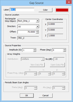
A gap is an infinitesimally narrow discontinuity that is placed on the path of current flow on a feed line. In planar structures, feed lines are typically in the form of a microstrip, stripline, slotline or coplanar waveguide (CPW). You use rectangle strip objects to construct such feed lines. A gap source can be placed on any rectangle strip object on a PEC, PMC or conductive sheet trace. Depending on the type of the trace on which a gap source is placed, it will have a different physical interpretation.
A rectangle strip object on a PEC or conductive sheet trace can be regarded as a strip transmission line that carries electric currents along its length (local X direction). The characteristic impedance of the line is a function of its width (local Y direction). A gap source is placed somewhere along the length and across the width of such a rectangle strip object, thus creating an infinitesimally narrow gap at its location. In this case, the gap source represents an ideal voltage source in series with a lumped impedance that is connected across the gap to excite the strip transmission line. When the impedance is zero, the gap acts like an ideal lumped source and creates a uniform electric field across the gap. The source pumps electric current into the line. If the voltage source is shorted (having a zero amplitude), then the gap acts like a series lumped element on the transmission line.
A rectangle strip object on a PMC trace can be regarded as a slot transmission line on an infinite PEC ground plane that carries a magnetic current along its length (local X direction). The characteristic impedance of the slot line is a function of its width (local Y direction). A slot gap source is placed somewhere along the length and across the width of the rectangle strip object on a PMC trace and creates an infinitesimally narrow gap at its location. In this case, the slot gap source represents an ideal current source with a shunt lumped admittance that is connected across the slot to excite the slot transmission line. When the admittance is zero, the gap acts like an ideal current filament, which creates electric fields across the slot, equivalent to a magnetic current flowing into the slot line. If the current source is open (having a zero amplitude), then the gap acts like a shunt (parallel) lumped element on the slot line. As you will see later, a coplanar waveguide (CPW) can be realized using two parallel slot lines with two aligned, collocated gap sources.
To define a gap source, follow these steps:
- Open the Gap Source Dialog by right clicking on the Gap Sources item in the Sources section of the Navigation Tree and selecting Insert New Source...
- In the Source Location section of the dialog, you will find a list of all the Rectangle Strip Objects available in the project workspace. Select the desired host rectangle strip object. The box labeled Direction shows the direction or polarity of the new gap source on its host rectangle strip object. You have the option to select either the positive or negative direction for the source polarity.
- In the box labeled Offset, enter the distance of the gap source from the start point of the rectangle strip feed line. The value of Offset by default is initially set to the center of the line. As you change the offset value, you can see the gap move on its host object.
- In the Source Properties section, you can specify the Source Amplitude in Volts (or in Amperes in the case of a gap on a slot trace) and Phase in degrees.
- You can also change the default label as well as the default color of the gap source using the Color button of the dialog and selecting the desired color from the color palette.
Probe Sources
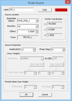
Another way of exciting a planar structure is by placing a gap on the path of a vertical current on a PEC via. This represents a filament source, which is used to model coaxial probe excitation. A probe source can be placed only on a PEC via object. Most planar transmission lines are fed using SMA connectors. The outer conductor of the coaxial line is connected to the ground and its inner conductor is extended across the substrate layer and connected to a metallic line. EM.Cube's Planar Module models a coaxial probe as an infinitesimal gap discontinuity placed across a thin via, representing an ideal voltage source in series with a lumped impedance. When the impedance is zero, the gap acts like an ideal lumped source and creates a uniform electric field across the via. The source pumps vertical electric current into the probe. If the voltage source is shorted (having a zero amplitude), then the gap acts like a shunt lumped element across the via.
To define a probe source, follow these steps:
- Open the Probe Source Dialog by right clicking on the Probe Sources item in the Sources section of the Navigation Tree and selecting Insert New Source...
- In the Source Location section of the dialog, in the dropdown list labeled Embedded Objects, you will find a list of all the PEC via objects available in the project workspace. Select the desired host PEC via object. The box labeled Direction shows the direction or polarity of the new probe source on its host PEC via object. You have the option to select either the positive or negative direction for the source.
- In the box labeled Offset, enter the distance of the probe source from the bottom of the via object. The value of Offset by default is initially set to the center of the via.
- In the Source Properties section, you can specify the Source Amplitude in Volts and Phase in degrees.
Unlike gap sources, whose offset parameter determines their exact location on their host line, the offset parameter of a probe source is not relevant except for long host vias. In the case of a short via that is discretized using a single prismatic element across its host substrate layer, the probe gap is always placed at the middle of its height. Longer vias may have a mesh that consists of two or more stacked prismatic elements. In this case, the probe source's offset determines which prismatic element will host the probe gap discontinuity at its middle.
Defining Source Arrays
If the project workspace contains an array of rectangle strip objects, the array object will also be listed as an eligible object for gap source placement. A gap source will then be placed on each element of the array. All the gap sources will have identical direction and offset. Similarly, if the project workspace contains an array of PEC via objects, the embedded array object will also be listed as an eligible object for probe source placement. A probe source will then be placed on each via object of the array. All the probe sources will have identical direction and offset.
However, you can prescribe certain amplitude and/or phase distribution over the array of gap or probe sources. By default, all the gap or probe sources have identical amplitudes of 1V (or 1A for the slot case) and zero phase. The available amplitude distributions to choose from include Uniform, Binomial and Chebyshev and Date File. In the Chebyshev case, you need to set a value for minimum side lobe level (SLL) in dB. You can also define Phase Progression in degrees along all three principal axes. You can view the amplitude and phase of individual sources by right clicking on the top Sources item in the Navigation Tree and selecting Show Source Label from the contextual menu.
Figure 1: Defining gap sources on an array of rectangle strip objects with a Chebyshev amplitude distribution.
In the data file option, the complex amplitude are directly read in from a data file using a real - imaginary format. When this option is selected, you can either improvise the complex array weights or import them from an existing file. In the former case click the New Data File button. This opens up the Windows Notepad with default formatted data file that has a list of all the array element indices with default 1+j0 amplitudes for all of them. You can replace the default complex values with new one and save the Notepad data file, which brings you back to the Gap Source dialog. To import the array weights, click the Open Data File button, which opens the standard Windows Open dialog. You can then select the right data file from the one of your folders. It is important to note that the data file must have the correct format to be read by EM.Cube. For this reason, it is recommended that you first create a new data file with the right format using Notepad as described earlier and then save it for later use.
Figure 2: Defining gap source array weights using a data file.
Defining Ports
Ports are used in a planar structure to order and index the sources for calculation of circuit parameters such as scattering (S), impedance (Z) and admittance (Y) parameters. In EM.Cube's Planar Module, you can use the following types of sources to define ports:
- Gap Sources
- Probe Sources
- Active Lumped Elements
- De-Embedded Sources
Ports are defined in the Observables section of the Navigation Tree. Right click on the Port Definition item of the Navigation Tree and select Insert New Port Definition... from the contextual menu. The Port Definition Dialog opens up, showing the default port assignments. If you have N sources in your planar structure, then N default ports are defined, with one port assigned to each source according to their order on the Navigation Tree. Note that your project can have mixed gap and probes sources as well as active lumped element sources.
Figure 1: The Port Definition dialog.
You can define any number of ports equal to or less than the total number of sources in your project. The Port List of the dialog shows a list of all the ports in ascending order, with their associated sources and the port's characteristic impedance, which is 50S by default. You can delete any port by selecting it from the Port List and clicking the Delete button of the dialog. Keep in mind that after deleting a port, you will have a source in your project without any port assignment and make sure that is what you intend. You can change the characteristic impedance of a port by selecting it from the Port List and clicking the Edit button of the dialog. This opens up the Edit Port dialog, where you can enter a new value in the box labeled Impedance.
Figure 2: Edit Port dialog.
Modeling Coupled Ports
Sources can be coupled to each other to model coupled strip lines (CPS) on metal traces or coplanar waveguides (CPW) on slot traces. Similarly, probe sources may be coupled to each other. Coupling two or more sources does not change the way they excite a planar structure. It is intended only for the purpose of S parameter calculation. The feed lines or vias which host the coupled sources are usually parallel and aligned with one another and they are all grouped together as a single transmission line represented by a single port. This single "coupled" port then interacts with other coupled or uncoupled ports.
You couple two or more sources using the Port Definition Dialog. To do so, you need to change the default port assignments. First, delete all the ports that are to be coupled from the Port List of the dialog. Then, define a new port by clicking the Add button of the dialog. This opens up the Add Port dialog, which consists of two tables: Available sources on the left and Associated sources on the right. A right arrow (-->) button and a left arrow (<--) button let you move the sources freely between these two tables. You will see in the "Available" table a list of all the sources that you deleted earlier. You may even see more available sources. Select all the sources that you want to couple and move them to the "Associated" table on the right. You can make multiple selections using the keyboard's Shift and Ctrl keys. Closing the Add Port dialog returns you to the Port Definition dialog, where you will now see the names of all the coupled sources next to the name of the newly added port.
| |
It is your responsibility to set up coupled ports and coupled transmission lines properly. For example, to excite the desirable odd mode of a coplanar waveguide (CPW), you need to create two rectangular slots parallel to and aligned with each other and place two gap sources on them with the same offsets and opposite polarities. To excite the even mode of the CPW, you use the same polarity for the two collocated gap sources. Whether you define a coupled port for the CPW or not, the right definition of sources will excite the proper mode. The couple ports are needed only for correct calculation of the port characteristics. |
Figure 1: Coupling gap sources in the Port Definition dialog by associating more than one source with a single port.
Calculating Port Characteristics At Gap Discontinuities
A gap source on a metal trace and a probe source on a PEC via behave like a series voltage source with a prescribed strength (of 1V and zero phase by default) that creates a localized discontinuity on the path of electric current flow. At the end of a planar MoM simulation, the electric current passing through the voltage source is computed and integrated to find the total input current. From this one can calculate the input admittance as
- [math] Y_{in} = \frac{I_{in}}{V_s} = \frac {\int_W \hat{y} \cdot \mathbf{J_s} \, dy} {V_s} [/math]
for gap sources on metal traces, where the line integration is performed across the width of the metal strip, and
- [math] Y_{in} = \frac{I_{in}}{V_s} = \frac {\int_S \hat{z} \cdot \mathbf{J_p} \, ds} {V_s} [/math]
for probe sources on PEC vias, where the surface integration is performed over the cross section of the via. On the other hand, a gap source on a slot trace behaves like a shunt current source with a prescribed strength (of 1A and zero phase by default) that creates a localized discontinuity on the path of magnetic current flow. At the end of a planar MoM simulation, the magnetic current passing through the current source is computed and integrated to find the total input voltage across the current filament. From this one can calculate the input impedance as
- [math] Z_{in} = \frac{V_{in}}{I_s} = \frac{\int_W \hat{y} \cdot \mathbf{M_s} \,dy} {V_s} = \frac{\int_W E_y \, dy}{V_s} [/math]
Note that the input admittance or impedance defined at a gap source port is referenced to the two terminals of the voltage source connected across the gap as shown in the figure below. This is different than the input admittance or impedance that one may normally define for a microstrip port, which is referenced to the substrate's ground.
Definition of different input impedances at the gap location.
To resolve this problem, you can place a gap source on a metal strip line by a distance of a quarter guide wavelength (λg/4) away from its open end. Note that (λg = 2p/ß), where ß is the propagation constant of the metallic transmission line. As show in the figure below, the impedance looking into an open quarter-wave line segment is zero, which effectively shorts the gap source to the planar structure's ground. The gap admittance or impedance in this case is identical to the input admittance or impedance of the planar structure.
Placing a gap source a quarter guide wavelength away from the open end of a feed line to effectively short it to the ground at the gap location.
The same principle applies to the gap sources on slot traces. The figure below shows how to place two gap sources with opposite polarities a quarter guide wavelength away from their shorted ends to calculate the correct input impedance of the CPW line looking to the left of the gap sources. Note that in this case, you deal with shunt filament current sources across the two slot lines and that the slot line carry magnetic currents. The end of the slot lines look open to the magnetic currents, but in reality they short the electric field. The quarter-wave CPW line acts as an open circuit to the current sources.
Placing two oppositely polarized gap sources a quarter guide wavelength away from the short end of a CPW line to effectively create an open circuit beyond the gap location.
The case of a probe source placed on a PEC via that is connected to a ground plane is more straightforward. In this case, the probe source's gap discontinuity is placed at the middle plane of the PEC via. If the via is short, it is meshed using a single prismatic element, which is connected to the ground from one side and to the metal strip line from the other. Therefore, the probe admittance or impedance is equal to that of the structure at a reference plane that passed through the host via.
Input impedance of a probe source on a PEC via connected to a ground plane.
Exciting Multiport Structures Using Linear Superposition
If your planar structure has two or more sources, but you have not defined any ports, all the lumped sources excite the structure locally and contribute to the excitation vector needed for the MoM solution of the problem. However, when you assign N ports to the sources, then you have a multiport structure that is characterized by an N×N admittance matrix (instead of a single Yin parameter), or an N×N impedance matrix, or an N×N scattering matrix. To calculate these matrices, EM.Cube uses a binary excitation scheme in conjunction with the principle of linear superposition. In this binary scheme, the structure is analyzed N times. Each time one of the N port-assigned sources is excited, and all the other port-assigned sources are turned off.
In the case of gap sources on metal traces and probe sources on PEC vias, turning a source off means shorting a series voltage source. The electric currents passing through these sources are then found at each port location, and the admittance parameters are found as follows:
- [math] I_m = \sum_{n=1}^N Y_{mn} V_n, \quad \quad Y_{mn} = \frac{I_m}{V_n} \bigg|_{V_k=0, k \ne n}[/math]
In the case of gap sources on slot traces, turning a source off means opening a shunt filament current source. The magnetic currents passing through the source locations, and thus the voltages across them, are then found at all ports, and the impedance parameters are found as follows:
- [math] V_m = \sum_{n=1}^N Z_{mn} I_n, \quad \quad Z_{mn} = \frac{V_m}{I_n} \bigg|_{I_k=0, k \ne n}[/math]
The N solution vectors that are generated through the N binary excitation analyses are finally superposed to produce the actual solution to the problem. However, in this process, EM.Cube also calculates all the port characteristics. Keep in mind that the impedance (Z) and admittance (Y) matrices are inverse of each other. From the impedance matrix, the scattering matrix is calculated using the following relation:
- [math] \mathbf{[S] = [Y_0] \cdot ([Z]-[Z_0]) \cdot ([Z]+[Z_0])^{-1} \cdot [Z_0]} [/math]
where [math]\mathbf{[Z_0]}[/math] and [math]\mathbf{[Y_0]}[/math] are diagonal matrices whose diagonal elements are the port characteristic impedances and admittances, respectively.
Modeling Lumped Elements In Planar MoM
Lumped elements are components, devices, or circuits whose overall dimensions are very small compared to the wavelength. As a result, they are considered to be dimensionless compared to the dimensions of a mesh cell. In fact, a lumped element is equivalent to an infinitesimally narrow gap that is placed in the path of current flow, across which the device's governing equations are enforced. Using Kirkhoff's laws, these device equations normally establish a relationship between the currents and voltages across the device or circuit. Crossing the bridge to Maxwell's domain, the device equations must now be cast into a from o boundary conditions that relate the electric and magnetic currents and fields. EM.Cube's Planar Module allows you to define passive circuit elements: Resistors(R), Capacitors(C), Inductors(L), and series and parallel combinations of them as shown in the figure below:
Figure 1: A series-parallel RLC combination that can be modeled as a lumped circuit in Planar Module.
Lumped elements are conceptualized in a similar way as gap or probe sources. They are indeed considered as infinitesimally narrow gaps placed in the path of current flow, across which Ohm's law is enforced. If a lumped element is placed on a PEC or conductive sheet trace, it is treated as a series connection. The boundary condition at the location of the lumped element is:
- [math] V_{gap} = Z_L I_{in} \quad\quad \int_{\delta} \hat{x}\cdot \mathbf{E_{gap}} \, dx = Z_L \int_W \hat{y} \cdot \mathbf{J_s} \, dy [/math]
where ZL is the total impedance across the two terminals of the series element. If the lumped element is placed on a slot trace, it is treated as a shunt connection that creates a current discontinuity. In this case, the magnetic current across the gap is continuous, and the boundary condition at the location of the lumped element is:
- [math] I_{gap} = Y_L V_{in} \quad\quad \int_{\delta} J_Y^{fila} \, dx = Y_L \int_W E_y \, dy [/math]
- [math] \int_{\delta} \hat{x}\cdot\hat{n} \times (\mathbf{H_{gap}^+ - H_{gap}^-}) \, dx = Y_L \int_W \hat{y}\cdot\mathbf{M_s} \, dy [/math]
where YL is the total admittance across the two terminals of the shunt element. If a lumped element is placed on a PEC via that is connected to a metal strip from one side and to a PEC ground plane from the other end, it is indeed as a series connection across a gap discontinuity at the middle plane of the via. If the via is short, it is meshed using a single prismatic element. In that case, the lumped element in effect shunts the metal strip to the ground. The boundary condition at the location of the lumped element across the PEC via is:
- [math] V_{gap} = Z_L I_{in} \quad\quad \int_{\delta} \hat{z}\cdot \mathbf{E_{gap}} \, dz = Z_L \int_S \hat{z} \cdot \mathbf{J_p} \, ds [/math]
Figure 1: Using a shunt lumped element on a PEC via to terminate a metallic strip line.
Defining Lumped Circuits
To define a lumped RLC circuit in your planar structure, follow these steps:
- Open the Lumped Element Dialog by right clicking on the Lumped Elements item in the Sources section of the Navigation Tree and selecting Insert New Source...
- In the Gap Topology section of the dialog, select one of the two options: Gap on Line and Gap on Via.
- In the Lumped Circuit Type section of the dialog, select one of the two options: Passive RLC and Active with Gap Source.
- Depending on your choice of gap topology, in the Lumped Circuit Location section of the dialog, you will find either a list of all the Rectangle Strip Objects or a list of all the PEC Via Objects available in the project workspace. Select the desired rectangle strip or embedded PEC via object.
- In the box labeled Offset, enter the distance of the lumped element from the start point of the rectangle strip line or from the bottom of the via object, whichever the case. The value of Offset by default is initially set to the center of the line or via.
- In the Load Properties section, the series and shunt resistance values Rs and Rp are specified in Ohms, the series and shunt inductance values Ls and Lp are specified in nH (nanohenry), and the series and shunt capacitance values Cs and Cp are specified in pF (picofarad). Only the checked elements are taken into account in the total impedance calculation. By default, only the series resistor is checked with a value of 50S, and all other circuit elements are initially greyed out.
EM.Cube's Planar Module allows you to define a voltage source in series with a series-parallel RLC combination and place them across the gap. This is called an active lumped element. If you choose the Active with Gap Source option of the Lumped Circuit Type section of the dialog, the right section of the dialog entitled Source Properties becomes enabled, where you can you can specify the Source Amplitude in Volts (or in Amperes in the case of PMC traces) and the Phase in degrees. Also, the box labeled Direction becomes relevant in this case which contains a gap source. Otherwise, a passive RLC circuit does not have polarity.
If the project workspace contains an array of rectangle strip objects or PEC via objects, the array object will also be listed as an eligible object for lumped element placement. A lumped element will then be placed on each element of the array. All the lumped elements will have identical direction, offset, resistance, inductance and capacitance values. If you define an active lumped element, you can prescribe certain amplitude and/or phase distribution to the gap sources just like in the case of gap and probe sources. The available amplitude distributions include Uniform', Binomial', Chebyshev and Data File.
Calculating Scattering Parameters Using Prony's Method
The calculation of the scattering (S) parameters is usually an important objective of modeling planar structures especially for planar circuits like filters, couplers, etc. As you saw earlier, you can use lumped sources like gaps and probes and even active lumped elements to calculate the circuit characteristics of planar structures. The admittance / impedance calculations based on the gap voltages and currents are accurate at RF and lower microwave frequencies or when the port transmission lines are narrow. In such cases, the electric or magnetic current distributions across the width of the port line are usually smooth, and quite uniform current or voltage profiles can easily be realized. At higher frequencies, however, a more robust method is needed for calculating the port parameters.
One can calculate the scattering parameters of a planar structure directly by analyzing the current distribution patterns on the port transmission lines. The discontinuity at the end of a port line typically gives rise to a standing wave pattern that can clearly be discerned in the line's current distribution. From the location of the current minima and maxima and their relative levels, one can determine the reflection coefficient at the discontinuity, i.e. the S11 parameter. A more robust technique is Prony’s method, which is used for exponential approximation of functions. A complex function f(x) can be expanded as a sum of complex exponentials in the following form:
- [math] f(x) \approx \sum_{n=1}^N c_i e^{-j\gamma_i x} [/math]
where ci are complex coefficients and γi are, in general, complex exponents. From the physics of transmission lines, we know that lossless lines may support one or more propagating modes with pure real propagation constants (real γi exponents). Moreover, line discontinuities generate evanescent modes with pure imaginary propagation constants (imaginary γi exponents) that decay along the line as you move away from the location of such discontinuities.
In practical planar structures for which you want to calculate the scattering parameters, each port line normally supports one, and only one, dominant propagating mode. Multi-mode transmission lines are seldom used for practical RF and microwave applications. Nonetheless, each port line carries a superposition of incident and reflected dominant-mode propagating signals. An incident signal, by convention, is one that propagates along the line towards the discontinuity, where the phase reference plane is usually established. A reflected signal is one that propagates away from the port plane. Prony's method can be used to extract the incident and reflected propagating and evanescent exponential waves from the standing wave data. From a knowledge of the amplitudes (expansion coefficients) of the incident and reflected dominant propagating modes at all ports, the scattering matrix of the multi-port structure is then calculated. In Prony's method, the quality of the S parameter extraction results depends on the quality of the current samples and whether the port lines exhibit a dominant single-mode behavior. Clean current samples can be drawn in a region far from sources or discontinuities, typically a quarter wavelength away from the two ends of a feed line.
Figure 1: Minimum and maximum current locations of the standing wave pattern on a microstrip line feeding a patch antenna.
De-Embedded Sources

EM.Cube's Planar Module provides de-embedded sources for the exclusive purpose of accurate S parameter calculation based on Prony's method. A de-embedded source is indeed a gap source that is placed close to an open end of a feed line. The other end of the line is typically connected to a planar structure of interest. Like gap sources, de-embedded sources can be placed only on rectangle strip objects. During mesh generation, EM.Cube automatically extends the length of a port line that hosts a de-embedded source to about two effective wavelengths. This is done to provide enough length for formation of a clean standing wave current pattern. The effective wavelength of a transmission line for length extension purposes is calculated in a similar manner as for the planar mesh resolution. It is defined as [math]\lambda_{eff} = \tfrac{\lambda_0}{\sqrt{\varepsilon_{eff}}}[/math], where εeff is the effective permittivity. For metal and conductive sheet traces, the effective permittivity is defined as the larger of the permittivities of the two substrate layers just above and below the metallic trace. For slot traces, the effective permittivity is defined as the mean (average) of the permittivities of the two substrate layers just above and below the metallic trace. The host port line must always be open from one end to allow for its length extension. You have to make sure that there are no objects standing on the way of the extended port line to avoid any unwanted overlaps.
Figure 1: The mesh of a patch antenna excited with a de-embedded source. Note the feed line extension in the mesh view.
You can define de-embedded source on metal (PEC), slot (PMC) and conductive sheet traces. To define a de-embedded source, follow these steps:
- Open the De-Embedded Source Dialog by right clicking on the De-Embedded Sources item in the Sources section of the Navigation Tree and selecting Insert New Source...
- In the Source Location section of the dialog, you will find a list of all the Rectangle Strip Objects or arrays of such objects that are available in the project workspace. The box labeled Direction shows the direction the phase reference plane for S parameter calculation and determines which end of the host line to place the source at. You have the option to select either the positive or negative direction to bounce the source between the two ends of the line.
- In the box labeled Offset, enter the distance of the phase reference plane from the end of the feed line object. The value of Offset by default is initially set to zero, meaning that the S parameters are calculated at the plane passing through the end of the feed line. Type in a new offset value or use the spin buttons to move the source arrow along the line away from its end. As you change the offset value, you can see the source arrow move along its host object.
- In the Source Properties section, you can specify the Source Amplitude in Volts (or in Amperes in the case of slot traces) and Phase in degrees.
- In the Prony Mode Extraction section, you can specify the Number of Prony Modes, which refers to the number of positive-negative exponential pairs that are extracted from the standing wave current data. The default value is 1 and represents the dominant quasi-TEM incident/reflected signal pair.
In a planar project with de-embedded sources, if you do not define any ports, the feed lines will simply be extended, and the exciting gap sources will be placed at the open ends of these extended lines. Note that if you define a de-embedded source along with a port definition in your project, then all the other port-assigned sources of your project must be of the same de-embedded type. You can define de-embedded sources for coplanar waveguides (CPW) on slot traces. To do so, you need to place two collocated, de-embedded sources with identical offsets (same phase reference plane), same source amplitudes but 180° phase difference. Note that for CPW structures, setting the number of Prony modes to 2 can get you more accurate results. In this case, the two extracted Prony modes will include the incident and reflected, odd and even, propagating modes of the CPW.
Using the Line Calculator
EM.Cube's Planar Module provides a simple calculator for analyzing planar transmission lines. It is based on the frequency domain finite difference (FDFD) technique. You can find the characteristic impedance, effective permittivity and guide wavelength of a TEM or quasi-TEM transmission line defined based on your project's background structure. Therefore, any arbitrary stack-up configuration with any number of substrate layers can be considered.
To access the Line Calculator, first you have to select a metal (PEC) trace or a slot (PMC) trace in the Navigation Tree. Right click on the name of a trace and select Line Calc... from the contextual menu to open the Line Calc Dialog. You can analyze a metal strip line on any PEC trace or a coplanar waveguide (coupled slot lines) on any PMC trace. The 2D line structure to be analyzed by the FDFD method consists of the background structure of your project with a metal strip or CPW located at the Z-plane of your selected trace. Depending on whether your open the Line Calc dialog from a metal trace or a slot trace, a picture of a microstrip line or a CPW line appear at the top of the dialog, respectively. In the former case, you have to specify Strip Width in the project units. In the latter case, you have to specify Slot Width, too. Keep in mind that the strip width is equal to the spacing between the two slot lines minus the width of individual slot lines. Clicking the Analyze button of the dialog evokes the FDTD simulator, and calculated results are reflected in the boxes labeled Zo, Effective Permittivity and Guide Wavelength.
When your background structure involves a slot (PMC) trace, then there is an infinite PEC ground plane at the plane of the slot trace. In that case, when you analyze a strip line on a metal trace, you must keep in mind that your stack-up configuration will be truncated by the slot's ground plane just for purpose of Zo calculation. A typical case of this type is a slot-coupled patch antenna fed by a microstrip line underneath the slot. From the point of view of the Line Calculator, the microstrip line lies on a substrate layer that is backed by the slot's ground plane and it does not see the substrate layer lying above the slot plane.
Figure 1: Analyzing a metal strip line using the line calculator.
Figure 2: Analyzing a coplanar waveguide using the line calculator.
Short Dipole Sources
A short dipole is the simplest type of radiator, which consists of a short current element of length &DELTA;l, aligned along a unit vector û and carrying a current of I Amperes. The product I&DELTA;l is often called the dipole moment and gives a measure of the radiator's strength. A short dipole in the free space generates an azimuth-symmetric, almost omni-directional, far field. However, the radiated fields of a short dipole above a layered planar background structure are greatly altered by the presence of the substrate layers. Note that the electric and magnetic field radiated by a short dipole in the presence of a layered background structure are indeed nothing but the dyadic Green's functions of that structure:
- [math] E^{inc}(r) = \int_{\Delta_L} \overline{\overline{G_{EJ}}}(r|r') \cdot (I\Delta l \hat{u}) \, dl' [/math]
- [math] H^{inc}(r) = \int_{\Delta_L} \overline{\overline{G_{HJ}}}(r|r') \cdot (I\Delta l \hat{u}) \, dl' [/math]
To define a short dipole source, follow these steps:
- Right click on the Short Dipoles item in the Sources section of the Navigation Tree and select Insert New Source... The Short Dipole Dialog opens up.
- In the section titled Source Location, enter values for the X, Y and Z coordinates of the dipole's center. By default, a new dipole is placed at the origin of coordinates. As you change the coordinates using the spin buttons, you will see the dipole move in the project workspace.
- In the section titled Source Properties, you can change the values of the dipole's Amplitude (in A), Phase (in degrees) and Length in the project's length units. A new dipole, by default, is Z-directed. You can change its orientation by entering the components of its unit vector in the three boxes labeled Direction Unit Vector.
Plane Wave Sources
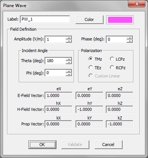
You can excite a planar structure with an incident plane wave to explore its scattering characteristics such as radar cross section (RCS). Exciting an antenna structure with an incident plane wave is equivalent to operating it in the "receive" mode. Plane wave excitation in the Planar Module is particularly useful for calculation of reflection and transmission coefficients of periodic surfaces. Note that the incident plane wave in your project bounces off the layered background structure and part of it also penetrates the substrate layers. The total incident field that is used to calculate the excitation vector of the MoM linear system is a superposition of the incident, reflected and transmitted plane waves at various regions of your planar structure:
- [math] \mathbf{E^{inc}(r)} = E_0 (\mathbf{\hat{e}_1} e^{ -jk_0 \mathbf{\hat{k}_1\cdot r} } + R \mathbf{\hat{e}_2} e^{ -jk_0 \mathbf{\hat{k}_2\cdot r} } ) [/math]
- [math] \mathbf{H^{inc}(r)} = \frac{E_0}{\eta_0} ( \mathbf{\hat{k}_1 \times \hat{e}_1} e^{-jk_0 \mathbf{\hat{k}_1 \cdot r} } + R \mathbf{\hat{k}_2 \times \hat{e}_2} e^{-jk_0 \mathbf{\hat{k}_2\cdot r} } ) [/math]
where [math]\eta_0 = 120\pi[/math] is the characteristic impedance of the free space, k1 and k2 are the unit propagation vectors of the incident plane wave and the wave reflected off the topmost substrate layer, respectively, and ê1 and ê2 are the polarization vectors corresponding to the electric field of those waves. R is the reflection coefficient at the interface between the top half-space and the topmost substrate layer and has different values for the TM and TE polarizations.
EM.Cube's Planar Module provides the following polarization options:
- TMz
- TEz
- LCPz
- RCPz
The direction of incidence is defined through the theta and phi angles of the propagation vector in the spherical coordinate system. The default values are θ = 180° and φ = 0°, representing a normally incident plane wave propagating along the -Z direction with a +X-polarized electric field vector. In the TMz and TEz polarization cases, the magnetic and electric fields are parallel to the XY plane, respectively. The left-hand (LCP) and right-hand (RCP) circular polarization cases are restricted to normal incidences only (θ = 180°).
To define a plane wave source, follow these steps:
- Right click on the Plane Waves item in the Sources section of the Navigation Tree and select Insert New Source... The Plane wave Dialog opens up.
- In the Field Definition section of the dialog, you can enter the Amplitude of the incident electric field in V/m and Phase in degrees. The default field Amplitude is 1 V/m, with a zero Phase.
- The direction of the Plane Wave is determined by the incident Theta and Phi angles expressed in the spherical coordinate system in degrees. You have to choose the Polarization of the plane wave from the four options: TMz, TEz, LCPzand RCPz. The components of the unit propagation vector are shown based on your choice of the angles of incidence. The components of the normalized E- and H-field vectors are also displayed based on your choice of polarization.
Running Planar MoM Simulations
The first step of planning a planar MoM simulation is defining your planar structure. This consists of the background structure plus all the finite-sized metal and slot trace objects and possibly embedded metal or dielectric objects that are interspersed among the substrate layers. The background stack-up is defined in the Layer Stack-up dialog, which automatically opens up as soon as you enter the Planar Module. The metal and slot traces and embedded object sets are listed in the Navigation Tree, which also shows all the geometrical (CAD) objects you draw in the project workspace under each object group at different Z-planes.
The next step is to decide on the excitation scheme. If your planar structure has one or more ports and you seek to calculate its port characteristics, then you have to choose one of the lumped source types or a de-embedded source. If you are interested in the scattering characteristics of your planar structure, then you must define a plane wave source. Before you can run a planar MoM simulation, you also need to decide on the project's observables. These are the simulation data that you expect EM.Cube to generate as the outcome of the numerical simulation. EM.Cube's Planar Module offers the following observables:
- Current Distribution
- Field Sensors
- Far Fields (Radiation Patterns or Radar Cross Section)
- Huygens Surfaces
- Port Characteristics
- Periodic Characteristics
If you run a simulation without having defined any observables, no data will be generated at the end of the simulation. Some observables require a certain type of excitation source. For example, port characteristics will be calculated only if the project contains a port definition, which in turn requires the existence of at least one gap or probe or de-embedded source. The periodic characteristics (reflection and transmission coefficients) are calculated only if the structure has a periodic domain and excited by a plane wave source.
Planar Module's Simulation Modes
The simplest simulation type in EM.Cube is an analysis. In this mode, the planar structure in your project workspace is meshed at the center frequency of the project. EM.Cube generates an input file at this single frequency, and the Planar MoM simulation engine is run once. Upon completion of the planar MoM simulation, a number of data files are generated depending on the observables you have defined in your project. An analysis is a single-run simulation.
EM.Cube offers a number of multi-run simulation modes. In such cases, the Planar MoM simulation engine is run multiple times. At each engine run, certain parameters are varied and a collection of simulation data are generated. At the end of a multi-run simulation, you can graph the simulation results in EM.Grid or you can animate the 3D simulation data from the Navigation Tree. For example, in a frequency sweep, the frequency of the project is varied over its specified bandwidth. Port characteristics are usually plotted vs. frequency, representing your planar structure's frequency response. In an angular sweep, the θ or φ angle of incidence of a plane wave source is varied over their respective ranges. EM.Cube's Planar Module currently provides the following types of multi-run simulation modes:
- Frequency Sweep
- Parametric Sweep
- Angular Sweep
- R/T Macromodel
- Huygens Sweep
- Optimization
- HDMR
Figure 1: Selecting a simulation mode in Planar Module's Simulation Run dialog.
Running A Planar MoM Analysis
To run a planar MoM analysis of your project structure, open the Run Simulation Dialog by clicking the Run ![]() button on the Simulate Toolbar or select Menu > Simulate > Run or use the keyboard shortcut Ctrl+R. The Analysis option of the Simulation Mode dropdown list is selected by default. Once you click the Run button, the simulation starts. A new window, called the Output Window, opens up that reports the different stages of simulation and the percentage of the tasks completed at any time. After the simulation is successfully completed, a message pops up and reports the end of simulation. In certain cases like calculating scattering parameters of a circuit or reflection / transmission characteristics of a periodic surface, some results are also reported in the Output Window. At the end of a simulation, you need to click the Close button of the Output Window to return to the project workspace.
button on the Simulate Toolbar or select Menu > Simulate > Run or use the keyboard shortcut Ctrl+R. The Analysis option of the Simulation Mode dropdown list is selected by default. Once you click the Run button, the simulation starts. A new window, called the Output Window, opens up that reports the different stages of simulation and the percentage of the tasks completed at any time. After the simulation is successfully completed, a message pops up and reports the end of simulation. In certain cases like calculating scattering parameters of a circuit or reflection / transmission characteristics of a periodic surface, some results are also reported in the Output Window. At the end of a simulation, you need to click the Close button of the Output Window to return to the project workspace.
Figure 1: Planar Module's Simulation Run dialog.
Stages Of A Planar MoM Analysis
EM.Cube's Planar MoM simulation engine uses a particular formulation of the method of moments called mixed potential integral equation (MPIE). Due to high-order singularities, the dyadic Green's functions for electric fields generated by electric currents as well as the dyadic Green's functions for magnetic fields generated by magnetic currents have very slow convergence behaviors. Instead of using these slowly converging dyadic Green's function, the MPIE formulation uses vector and scalar potentials. These include vector electric potential A(r), scalar electric potential KΦ(r), vector magnetic potential F(r) and scalar magnetic potential KΨ(r). These potentials have singularities of lower orders. As a result, they coverage relatively faster. The speed of their convergence is further increased drastically using special singularity extraction techniques.
A planar MoM simulation consists of two major stages: matrix fill and linear system inversion. In the first stage, the moment matrix and excitation vector are calculated. In the second stage, the MoM system of linear equations is inverted using one of the several available matrix solvers to find the unknown coefficients of all the basis functions. The unknown electric and magnetic currents are linear superpositions of all these elementary solutions. These can be visualized in EM.Cube using the current distribution observables. Having determined all the electric and magnetic currents in your planar structure, EM.Cube can then calculate the near fields on prescribed planes. These are introduced as field sensor observables. The near-zone electric and magnetic fields are calculated using a spectral domain formulation of the dyadic Green's functions. Finally the far fields of the planar structure are calculated in the spherical coordinate system. These calculations are performed using the asymptotic form of the dyadic Green's functions using the "stationary phase method".
Setting Numerical Parameters
A planar MoM simulation involves a number of numerical parameters that take preset default values unless you change them. You can access these parameters and change their values by clicking the Settings button next to the Select Engine dropdown list in the Planar Module's Simulation Run dialog. In most cases, you do not need to open this dialog and you can leave all the default numerical parameter values intact. However, it is useful to familiarize yourself with these parameters, as they may affect the accuracy of your numerical results.
The Planar MoM Engine Settings Dialog is organized in a number of sections. Here we describe some of the numerical parameters. The "Matrix Fill" section of the dialog deals with the operations involving the dyadic Green's functions. You can set a value for the Convergence Rate for Integration, which is 1E-5 by default. This is used for the convergence test of all the infinite integrals in the calculation of the Hankel transform of spectral-domain dyadic Green's functions. When the substrate is lossy, the surface wave poles are captured in the complex integration plane using contour deformation. You can change the maximum number of iterations involved in this deformed contour integration, whose default value is 20. When the substrate is very thin with respect to the wavelength, the dyadic Green's functions exhibit numerical instability. Additional singularity extraction measures are taken to avoid numerical instability but at the expense of increased computation time. By default, a thin substrate layer is defined to a have a thickness less than 0.01λeff, where λeff is the effective wavelength. You can modify the definition of "Thin Substrate" by entering a value for Thin Substrate Threshold different than the default 0.01. The parameter Max Coupling Range determines the distance threshold in wavelength between the observation and source points after which the Green's interactions are neglected. This distance by default is set to 1,000 wavelengths. For electrically small structures, the phase variation across the structure may be negligible. In such cases, a fast quasi-static analysis can be carried out. You can set this threshold in wavelengths in the box labeled Max Dimensions for Quasi-Static Analysis.
In the "Spectral Domain Integration" section of the dialog, you can set a value to Max Spectral Radius in k0, which has a default value of 30. This means that the infinite spectral-domain integrals in the spectral variable kρ are pre-calculated and tabulated up to a limit of 30k0, where k0 is the free space propagation constant. These integrals may converge much faster based on the specified Convergence Rate for Integration described earlier. However, in certain cases involving highly oscillatory integrands, much larger integration limits like 100k0 might be needed to warrant adequate convergence. For spectral-domain integration along the real kρ axis, the interval [0, Nk0] is subdivided into a large number of sub-intervals, within each an 8-point Gauss-Legendre quadrature is applied. The next parameter, No. Radial Integration Divisions per k0, determines how small these intervals should be. By default, 2 divisions are used for the interval [0, k0]. In other words, the length of each integration sub-interval is k0/2. You can increase the resolution of integration by increasing this value above 2. Finally, instead of 2D Cartesian integration in the spectral domain, a polar integration is performed. You can set the No. of Angular Integration Points, which has a default value of 100.
Figure 1: The Planar MoM Engine Settings dialog.
Planar Module's Linear System Solvers
After the MoM impedance matrix [Z] (not to be confused with the impedance parameters) and excitation vector [V] have been computed through the matrix fill process, the planar MoM simulation engine is ready to solve the system of linear equations:
- [math] \mathbf{[Z]}_{N\times N} \cdot \mathbf{[I]}_{N\times 1} = \mathbf{[V]}_{N\times 1} [/math]
where [I] is the solution vector, which contains the unknown amplitudes of all the basis functions that represent the unknown electric and magnetic currents of finite extents in your planar structure. In the above equation, N is the dimension of the linear system and equal to the total number of basis functions in the planar mesh. EM.Cube's linear solvers compute the solution vector[I] of the above system. You can instruct EM.Cube to write the MoM matrix and excitation and solution vectors into output data files for your examination. To do so, check the box labeled "Output MoM Matrix and Vectors" in the Matrix Fill section of the Planar MoM Engine Settings dialog. These are written into three files called mom.dat1, exc.dat1 and soln.dat1, respectively.
There are a large number of numerical methods for solving systems of linear equations. These methods are generally divided into two groups: direct solvers and iterative solvers. Iterative solvers are usually based on matrix-vector multiplications. Direct solvers typically work faster for matrices of smal to medium size (N<3,000). EM.Cube's Planar Module offers five linear solvers:
- LU Decomposition Method
- Biconjugate Gradient Method (BiCG)
- Preconditioned Stabilized Biconjugate Gradient Method (BCG-STAB)
- Generalized Minimal Residual Method (GMRES)
- Transpose-Free Quasi-Minimum Residual Method (TFQMR)
Of the above list, LU is a direct solver, while the rest are iterative solvers. BiCG is a relatively fast iterative solver, but it works only for symmetric matrices. You cannot use BiCG for periodic structures or planar structures that contain both metal and slot traces at different planes, as their MoM matrices are not symmetric. The three solvers BCG-STAB, GMRES and TtFQMR work well for both symmetric and asymmetric matrices and they also belong to a class of solvers called Krylov Sub-space Methods. In particular, the GMRES method always provides guaranteed unconditional convergence.
EM.Cube's Planar Module, by default, provides a "Automatic" solver option that picks the best method based on the settings and size of the numerical problem. For linear systems with a size less than N = 3,000, the LU solver is used. For larger systems, BiCG is used when dealing with symmetric matrices, and GMRES is used for asymmetric matrices. If the size of the linear system exceeds N = 15,000, the sparse version of the iterative solvers is used, utilizing a row-indexed sparse storage scheme. You can override the automatic solver option and manually set you own solver type. This is done using the Solver Type dropdown list in the "Linear System Solver" section of the Planar MoM Engine Settings dialog. There are also a number of other parameters related to the solvers. The default value of Tolerance of Iterative Solver is 1E-3, which can be increased for more ill-conditioned systems. The maximum number of iterations is usually expressed as a multiple of the systems size. The default value of Max No. of Solver Iterations / System Size is 3. For extremely large systems, sparse versions of iterative solvers are used. In this case, the elements of the matrix are thresholded with respect to the larges element. The default value of Threshold for Sparse Solver is 1E-6, meaning that all the matrix elements whose magnitude is less than 1E-6 times the large matrix elements are set equal to zero. There are two more parameters that are related to the Automatic Solver option. These are " User Iterative Solver When System Size >" with a default value of 3,000 and " Use SParse Storage When System Size > " with a default value of 15,000. In other words, you control the automatic solver when to switch between direct and iterative solvers and when to switch to the sparse version of iterative solvers.
If your computer has an Intel CPU, then EM.Cube offers special versions of all the above linear solvers that have been optimized for Intel CPU platforms. These optimal solvers usually work 2-3 time faster than their generic counterparts. When you install EM.Cube, the option to use Intel-optimized solvers is already enabled. However, you can disable this option (e.g. if your computer has a non-Intel CPU). To do that, open the EM.Cube's Preferences Dialog from Menu > Edit > Preferences or using the keyboard shortcut Ctrl+H. Select the Advanced tab of the dialog and uncheck the box labeled " Use Optimized Solvers for Intel CPU".
Visualizing Current Distributions
Electric and magnetic currents are the fundamental output data of a planar MoM simulation. After the numerical solution of the MoM linear system, they are found using the solution vector [I] and the definitions of the electric and magnetic vectorial basis functions:
- [math] \mathbf{[I]}_{N\times 1} = \begin{bmatrix} I^{(J)} \\ \\ V^{(M)} \end{bmatrix} \quad \Rightarrow \quad \begin{cases} \mathbf{J(r)} = \sum_{n=1}^N I_n^{(J)} \mathbf{f_n^{(J)} (r)} \\ \\ \mathbf{M(r)} = \sum_{k=1}^K V_k^{(M)} \mathbf{f_k^{(M)} (r)} \end{cases} [/math]
Note that currents are complex vector quantities. Each electric or magnetic current has three X, Y and Z components, and each complex component has a magnitude and phase. You can visualize the surface electric currents on metal (PEC) and conductive sheet traces, surface magnetic currents on slot (PMC) traces and vertical volume currents on the PEV vias and embedded dielectric objects. 3D color-coded intensity plots of electric and magnetic current distributions are visualized in the project workspace, superimposed on the surface of physical objects.
In order to view the current distributions, you must first define them as observables before running the planar MoM simulation. To do that, right click on the Current Distributions item in the Observables section of the Navigation Tree and select Insert New Observable.... The Current Distribution Dialog opens up. At the top of the dialog and in the section titled Active Trace / Set, you can select a trace or embedded object set where you want to observe the current distribution. You can also select the current map type from two options: Confetti and Cone. The former produces an intensity plot for current amplitude and phase, while the latter generates a 3D vector plot.
Figure 1: The Planar Module's Current Distribution dialog.
Once you close the current distribution dialog, the label of the selected trace or object set is added under the Current Distributions node of the Navigation Tree.
| |
You have to define a separate current distribution observable for each individual trace or embedded object set. |
At the end of a planar MoM simulation, the current distribution nodes in the Navigation Tree become populated by the magnitude and phase plots of the three vectorial components of the electric (J) and magnetic (M) currents as well as the total electric and magnetic currents defined in the following manner:
- [math] | \mathbf{J_{tot}} | = \sqrt{|J_x|^2 + |J_y|^2 + |J_z|^2}[/math]
- [math] | \mathbf{M_{tot}} | = \sqrt{|M_x|^2 + |M_y|^2 + |M_z|^2}[/math]
You can click on any current plot to visualize it in the project workspace. A legend box at the upper right corner of the screen shows the color map scale as well as the minimum, maximum, mean and standard deviation of the current data and its units. To exit the 3D plot view and return to EM.Cube's normal view, hit the keyboard's Esc Key.
Figure 2: The current distribution map of a patch antenna.
Figure 3: Vectorial (cone) visualization of the current distribution on a patch antenna.
Computing The Near Fields
Once all the current distributions are known in a planar structure, the electric and magnetic fields can be calculated everywhere in that structure using the dyadic Greens's functions of the background structure:
- [math] \begin{align} \mathbf{E(r) = E_{inc}(r)} + & \sum_{n=1}^N I_n^{(J)} \iiint_V \overline{\overline{G}}_{EJ}(r|r') \cdot f_n^{(J)}(r') \, d\nu' + \\ & \sum_{k=1}^K V_n^{(M)} \iiint_V \overline{\overline{G}}_{EM}(r|r') \cdot f_k^{(M)}(r') \, d\nu' \end{align} [/math]
- [math] \begin{align} \mathbf{H(r) = H_{inc}(r)} + & \sum_{n=1}^N I_n^{(J)} \iiint_V \overline{\overline{G}}_{HJ}(r|r') \cdot f_n^{(J)}(r') \, d\nu' + \\ & \sum_{k=1}^K V_n^{(M)} \iiint_V \overline{\overline{G}}_{HM}(r|r') \cdot f_k^{(M)}(r') \, d\nu' \end{align} [/math]
The above equations can be cast into the spectral domain as follows:
- [math] \begin{align} \mathbf{E(r) = E_{inc}(r)} + \frac{1}{(2\pi)^2} \int\limits_{-\infty}^{\infty} \int\limits_{-\infty}^{\infty} \bigg[ & \sum_{n=1}^N I_n^{(J)} \tilde{\overline{\overline{G}}}_{EJ}(k_{\rho}, z|z') \cdot \tilde{f}_n^{(J)}(k_x, k_y) + \\ & \sum_{k=1}^K V_n^{(M)} \tilde{\overline{\overline{G}}}_{EM}(k_{\rho}, z|z') \cdot \tilde{f}_k^{(M)}(k_x, k_y) \bigg] \, dk_x \, dk_y \end{align} [/math]
- [math] \begin{align} \mathbf{H(r) = H_{inc}(r)} + \frac{1}{(2\pi)^2} \int\limits_{-\infty}^{\infty} \int\limits_{-\infty}^{\infty} \bigg[ & \sum_{n=1}^N I_n^{(J)} \tilde{\overline{\overline{G}}}_{HJ}(k_{\rho}, z|z') \cdot \tilde{f}_n^{(J)}(k_x, k_y) + \\ & \sum_{k=1}^K V_n^{(M)} \tilde{\overline{\overline{G}}}_{HM}(k_{\rho}, z|z') \cdot \tilde{f}_k^{(M)}(k_x, k_y) \bigg] \, dk_x \, dk_y \end{align} [/math]
Calculation of the near-zone fields (fields at the vicinity of the unknown currents) is done at the post-processing stage and in a Cartesian coordinate systems. These calculations involve doubly infinite spectral-domain integrals, which are computed numerically. As was mentioned earlier, EM.Cube's planar MoM engine rather uses a polar integration scheme, where the radial spectral variable kρ is integrated over the interval [0, Mk0], M being a large enough number to represent infinity, and the angular spectral variable t is integrated over the interval [0, 2π]. You also saw some of the numerical parameters related to this spectral-domain integration scheme.
Visualizing The Near Fields

In order to view the near field distributions, you must first define field sensor observables before running the planar MoM simulation. To do that, right click on the Field Sensors item in the Observables section of the Navigation Tree and select Insert New Observable.... The Field Sensor Dialog opens up. At the top of the dialog and in the section titled Sensor Plane Location, first you need to set the plane of near field calculation. In the dropdown box labeled Direction, you have three options X, Y, and Z, representing the"normals" to the XY, YZ and ZX planes, respectively. The default direction is Z, i.e. XY plane parallel to the substrate layers. In the three boxes labeled Coordinates, you set the coordinates of the center of the plane. Then, you specify the Size of the plane in project units, and finally set the Number of Samples along the two sides of the sensor plane. The larger the number of samples, the smoother the near field map will appear.
In the section titled Output Settings, you can also select the field map type from two options: Confetti and Cone. The former produces an intensity plot for field amplitude and phase, while the latter generates a 3D vector plot. In the confetti case, you have an option to check the box labeled Data Interpolation, which creates a smooth and blended (digitally filtered) map. In the cone case, you can set the size of the vector cones that represent the field direction. At the end of a sweep simulation, multiple field map are produced and added to the Navigation Tree. You can animate these maps. However, during the sweep only one field type is stored, either the E-field or H-field. You can choose the field type for multiple plots using the radio buttons in the section titled Field Display - Multiple Plots. The default choice is the E-field.
Once you close the Field Sensor dialog, its name is added under the Field Sensors node of the Navigation Tree. At the end of a planar MoM simulation, the field sensor nodes in the Navigation Tree become populated by the magnitude and phase plots of the three vectorial components of the electric (E) and magnetic (H) field as well as the total electric and magnetic fields defined in the following manner:
- [math] |\mathbf{E_{tot}}| = \sqrt{|E_x|^2 + |E_y|^2 + |E_z|^2} [/math]
- [math] |\mathbf{H_{tot}}| = \sqrt{|H_x|^2 + |H_y|^2 + |H_z|^2} [/math]
Note that unlike EM.Cube's other computational modules, near field calculations in the Planar Module usually takes substantial time. This is due to the fact that at the end of a planar MoM simulation, the fields are not available anywhere (as opposed to the FDTD Module), and their computation requires integration of complex dyadic Green's functions (as opposed to MoM3D Module's free space Green's functions).
Near-zone electric field map above a microstrip-fed patch antenna.
Near-zone magnetic field map above a microstrip-fed patch antenna.
Computing The Far Fields
Unlike differential-based methods, MoM simulators do not need a radiation box to calculate the far field data. The far-zone fields are calculated directly by integrating the currents on the traces and across the embedded objects using the asymptotic form of the background structure’s dyadic Green's functions:
- [math] \mathbf{E^{ff}(r)} = \iiint_V \mathbf{ \overline{\overline{G}}_{EJ,ff}(r|r') \cdot J(r') } \, d\nu ' + \iiint_V \mathbf{ \overline{\overline{G}}_{EM,ff}(r|r') \cdot M(r') } \, d\nu '[/math]
- [math] \mathbf{H^{ff}(r)} = \dfrac{1}{\eta_0} \mathbf{ \hat{r} \times E^{ff}(r) }[/math]
where η0 = 120π is the characteristic impedance of the free space. As can be seen from the above equations, the far fields have the form of a TEM wave propagating in the radial direction away from the origin of coordinates. This means that the far-field magnetic field is always perpendicular to the electric field and the propagation vector, which in this case happens to be the radial unit vector in the spherical coordinate system. In other words, one only needs to know the far-zone electric field and can easily calculate the far-zone magnetic field from it. In EM.Cube's mixed potential integral equation formulation, the far-zone electric field can be expressed in terms of the asymptotic form of the vector electric and magnetic potentials A and F:
- [math]\mathbf{E^{ff}}(x,y,z) = j k_0 \eta_0 \hat{r} \times [\hat{r} \times \mathbf{A}(r \to \infty)] + j k_0 \hat{r} \times \mathbf{F}(r \to \infty)[/math]
The asymptotic form of these vector potentials are calculated using the "Method of Stationary Phase" when k0r → ∞. In that case, one can use the approximation:
- [math] k_0 |\mathbf{r-r'}| \approx k_0 (r - \mathbf{\hat{r} \cdot r'}) [/math]
After applying the stationary phase method, one can extract the spherical wave factor exp(-jk0r)/r from the far-zone electric field, leaving the rest as functions of the spherical angles θ and φ. In other words, the far field is normalized to r, the distance from the field observation point to the origin. It is customary to express the far fields in spherical components Eθ and Eφ. Note that the outward propagating, TEM-type, far fields do not have radial components, i.e. Er = 0.
- [math] \mathbf{E_{\theta}}(\theta, \phi) = \cos\theta \cos\phi E_x + \cos\theta \sin\phi E_y - \sin\theta E_z [/math]
- [math] \mathbf{E_{\phi}}(\theta, \phi) = -\sin\phi E_x + \cos\phi E_y [/math]
Visualizing The Far Fields

Even though the planar MoM engine does not need a radiation box, you still have to define a "Far Field" observable for radiation pattern calculation. This is because far field calculations take time and you have to instruct EM.Cube to perform these calculations. To define a far field, right click the Far Fields item in the Observables section of the Navigation Tree and select Insert New Radiation Pattern.... The Radiation Pattern Dialog opens up. You may accept the default settings, or you can change the value of Angle Increment, which is expressed in degrees. You can also choose to Normalize 2D Patterns. In that case, the maximum value of a 2D paten graph will have a value of 1; otherwise, the actual far field values in V/m will be used on the graph.
Once a planar MoM simulation is finished, three far field items are added under the Far Field item in the Navigation Tree. These are the far field component in θ direction, the far field component in φ direction and the "Total" far field. The 3D plots can be viewed in the project workspace by clicking on each item. The view of the 3D far field plot can be changed with the available view operations such as rotate view, pan, zoom, etc. If the structure blocks the view of the radiation pattern, you can simply hide or freeze the whole structure or parts of it. In a 3D radiation pattern plot, the fields are always normalized to the maximum value of the total far field for visualization purpose:
- [math]|\mathbf{E_{ff,tot}}| = \sqrt{ |E_{\theta}|^2 + |E_{\phi}|^2 }[/math]
Figure: 3D polar radiation pattern plot of a microstrip-fed patch antenna.
Figure: 3D vectorial (cone) radiation pattern plot of a microstrip-fed patch antenna.
The 2D radiation pattern graphs can be plotted from EM.Cube's Data Manager. A total of eight 2D radiation pattern graphs are available: 4 polar and 4 Cartesian graphs for the XY, YZ, ZX and user defined plane cuts.
Radar Cross Section of Planar Structures
When a planar structure is excited by a plane wave source, the calculated far field data indeed represent the scattered fields of that planar structure. EM.Cube can also calculate the radar cross section (RCS) of a planar target:
- [math] \sigma_{\theta} = 4\pi r^2 \dfrac{|E_{\theta}^{scat}|^2}{|E^{inc}|^2}, \quad \sigma_{\phi} = 4\pi r^2 \dfrac{|E_{\phi}^{scat}|^2}{|E^{inc}|^2}, \quad \sigma = \sigma_{\theta} + \sigma_{\phi} = 4\pi r^2 \dfrac{|E_{tot}^{scat}|^2}{|E^{inc}|^2} [/math]
Note that in this case the RCS is defined for a finite-sized target in the presence of an infinite background structure. The scattered θ and φ components of the far-zone electric field are indeed what you see in the 3D far field visualization of radiation (scattering) patterns. Instead of radiation or scattering patterns, you can instruct EM.Cube to plot 3D visualizations of σθ, σφ and the total RCS. To do so, you must define an RCS observable instead of a radiation pattern. Follow these steps:
- Right click on the Far Fields item in the Observables section of the Navigation Tree and select Insert New RCS... to open the Radar Cross Section Dialog.
- The resolution of RCS calculation is specified by Angle Increment expressed in degrees. By default, the θ and φ angles are incremented by 5 degrees.
- At the end of a planar MoM simulation, besides calculating the RCS data over the entire (spherical) 3D space, a number of 2D RCS graphs are also generated. These are RCS cuts at certain planes, which include the three principal XY, YZ and ZX planes plus one additional constant f-cut. This fourth plane cut is at φ = 45° by default. You can assign another φ angle in degrees in the box labeled Non-Principal Phi Plane.
At the end of a planar MoM simulation, in the far field section of the Navigation Tree, you will have the θ and φ components of RCS as well as the total radar cross section. You can view a 3D visualization of these quantities by clicking on their entries in the Navigation Tree. The RCS values are expressed in m2. The 3D plots are normalized to the maximum RCS value, which is also displayed in the legend box.
Figure 2: An example of the 3D mono-static radar cross section plot of a patch antenna.
Running a Frequency Sweep
In a frequency sweep, the operating frequency of a planar structure is varied during each sweep run. EM.Cube's Planar Module offers two types of frequency sweep: Uniform and Adaptive. In a uniform frequency sweep, the frequency range and the number of frequency samples are specified. The samples are equally spaced over the frequency range. At the end of each individual frequency run, the output data are collected and stored. At the end of the frequency sweep, the 3D data can be visualized and/or animated, and the 2D data can be graphed in EM.Grid.
To run a uniform frequency sweep, open the Simulation Run Dialog, and select the Frequency Sweep option from the dropdown list labeled Simulation Mode. When you choose the frequency sweep option, the Settings button next to the simulation mode dropdown list becomes enabled. Clicking this button opens the Frequency Settings dialog. The Frequency Rangeis initially set equal to your project's center frequency minus and plus half bandwidth. But you can change the values of Start Frequencyand End Frequency as well as the Number of Samples. The dialog offers two options for Frequency Sweep Type: Uniform or Adaptive. Select the former type. It is very important to note that in a MoM simulation, changing the frequency results in a change of the mesh of the structure, too. This is because the mesh density is defined in terms of the number of cells per effective wavelength. By default, during a frequency sweep, EM.Cube fixes the mesh density at the highest frequency, i.e., at the "End Frequency". This usually results in a smoother frequency response. You have the option to fix the mesh at the center frequency of the project or let EM.Cube "remesh" the planar structure at each frequency sample during a frequency sweep. You can make one of these three choices using the radio button in the Mesh Settings section of the dialog. Closing the Frequency Settings dialog returns you to the Simulation Run dialog, where you can start the planar MoM frequency sweep simulation by clicking the Run button.
Figure 1: Planar Module's Frequency Settings dialog.
Adaptive Frequency Sweep
Frequency sweeps are often performed to study the frequency response of a planar structure. In particular, the variation of scattering parameters like S11 (return loss) and S21 (insertion loss) with frequency are of utmost interest. When analyzing resonant structures like patch antennas or planar filters over large frequency ranges, you may have to sweep a large number of frequency samples to capture their behavior with adequate details. The resonant peaks or notches are often missed due to the lack of enough resolution. EM.Cube's Planar Module offers a powerful adaptive frequency sweep option for this purpose. It is based on the fact that the frequency response of a physical, causal, multiport network can be represented mathematically using a rational function approximation. In other words, the S parameters of a circuit exhibit a finite number of poles and zeros over a given frequency range. EM.Cube first starts with very few frequency samples and tries to fit rational functions of low orders to the scattering parameters. Then, it increases the number of samples gradually by inserting intermediate frequency samples in a progressive manner. At each iteration cycle, all the possible rational functions of higher orders are tried out. The process continues until adding new intermediate frequency samples does not improve the resolution of the "Sij" curves over the given frequency range. In that case, the curves are considered as having converged.
You must have defined one or more ports for your planar structure run an adaptive frequency sweep. Open the Frequency Settings dialog from the Simulation Run dialog and select the Adaptive option of Frequency Sweep Type. You have to set values for Minimum Number of Samples and Maximum Number of Samples. Their default values are 3 and 9, respectively. You also set a value for the Convergence Criterion, which has a default value of 0.1. At each iteration cycle, all the S parameters are calculated at the newly inserted frequency samples, and their average deviation from the curves of the last cycle is measured as an error. When this error falls below the specified convergence criterion, the iteration is ended. If EM.Cube reaches the specified maximum number of iterations and the convergence criterion has not yet been met, the program will ask you whether to continue the process or exit it and stop.
Figure 1: Settings adaptive frequency sweep parameters in Planar Module's Frequency Settings Dialog.
Examining Port Characteristics
If your planar structure is excited by gap sources or probe sources or de-embedded sources, and one or more ports have been defined, the planar MoM engine calculates the scattering, impedance and admittance (S/Z/Y) parameters of the designated ports. The scattering parameters are defined based on the port impedances specified in the project's Port Definition dialog. If more than one port has been defined in the project, the S/Z/Y matrices of the multiport network are calculated. Note that the S/Z/Y matrices of an N-port structure are related to each other through the following equations:
- [math]\mathbf{ [S] = [Y_0] \cdot ([Z]-[Z_0]) \cdot ([Z]+[Z_0])^{-1} \cdot [Z_0] }[/math]
- [math]\mathbf{ [Y] = [Z]^{-1} } [/math]
- [math]\mathbf{ [Z] = [\sqrt{Z_0}] \cdot ([U]+[S]) \cdot ([U]-[S])^{-1} \cdot [\sqrt{Z_0}] }[/math]
where [math]\mathbf{[U]}[/math] is the identity matrix of order N, [math]\mathbf{[Z_0]}[/math] and [math]\mathbf{[Y_0]}[/math] are diagonal matrices whose diagonal elements are the port characteristic impedances and admittances, respectively, and [math]\mathbf{[\sqrt{Z_0}]}[/math] is a diagonal matrix whose diagonal elements are the square roots of port characteristic impedances. The voltage standing wave ratio (VSWR) of the structure at the first port is also computed:
- [math]\text{VSWR} = \frac{|V_{max}|}{|V_{min}|} = \frac{1+|S_{11}|}{1-|S_{11}|}[/math]
At the end of a planar MoM simulation, the values of S/Z/Y parameters and VSWR data are calculated and reported in the output message window. The S, Z and Y parameters are written into output ASCII data files of complex type with a ".CPX" extension. Every file begins with a header consisting of a few comment lines that start with the "#" symbol. The complex values are arranged into two columns for the real and imaginary parts. In the case of multiport structures, every single element of the S/Z/Y matrices is written into a separate complex data file. For example, you will have data files like S11.CPX, S21.CPX, ..., Z11.CPX, Z21.CPX, etc. The VSWR data are saved to an ASCII data file of real type with a ".DAT" extension called, VSWR.DAT.
If you run an analysis, the port characteristics have single complex values, which you can view using EM.Cube's data manager. However, there are no curves to graph. You can plot the S/Z/Y parameters and VSWR data when you have data sets, which are generated at the end of any type of sweep including a frequency sweep. In that case, the ".CPX" files have multiple rows corresponding to each value of the sweep parameter (e.g. frequency). EM.Cube's 2D graph data are plotted in EM.Grid, a versatile graphing utility. You can plot the port characteristics directly from the Navigation Tree. Right click on the Port Definition item in the Observables section of the Navigation Tree and select one of the items: Plot S Parameters, Plot Y Parameters, Plot Z Parameters, or Plot VSWR. In the first three cases, another sub-menu gives a list of individual port parameters.
Figure 1: Selecting port characteristics data to plot from the Navigation Tree.
You can also see a list of all the port characteristics data files in EM.Cube's Data Manager. To open data manager, click the Data Manager ![]() button of the Simulate Toolbar or select Simulate > Data Manager from the menu bar, or right click on the Data Manager item of the Navigation Tree and select Open Data Manager... from the contextual menu. You can also use the keyboard shortcut Ctrl+D at any time. Select any data file by clicking and highlighting its row in the table and then click the Plot button to plot the graph. By default, the S parameters are plotted as double magnitude-phase graphs, while the Y and Z parameters are plotted as double real-imaginary part graphs. The VSWR data are plotted on a Cartesian graph. You can change the format of complex data plots. In general complex data can be plotted in three forms:
button of the Simulate Toolbar or select Simulate > Data Manager from the menu bar, or right click on the Data Manager item of the Navigation Tree and select Open Data Manager... from the contextual menu. You can also use the keyboard shortcut Ctrl+D at any time. Select any data file by clicking and highlighting its row in the table and then click the Plot button to plot the graph. By default, the S parameters are plotted as double magnitude-phase graphs, while the Y and Z parameters are plotted as double real-imaginary part graphs. The VSWR data are plotted on a Cartesian graph. You can change the format of complex data plots. In general complex data can be plotted in three forms:
- Magnitude and Phase
- Real and Imaginary Parts
- Smith Chart
Figure 2: EM.Cube's Data Manager showing a list of the port characteristics data files.
In particular, it may be useful to plot the Sii parameters on a Smith chart. To change the format of a data plot, select it in the Data Manager and click its Edit button. In the Edit File Dialog, choose one of the options provided in the dropdown list labeled Graph Type.
Figure 3: Changing the graph type by editing a data file's properties.
Figure 4: The S11 parameter plotted on a Smith Chart graph in EM.Grid.
Rational Interpolation Of Scattering Parameters
The adaptive frequency sweep described earlier is an iterative process, whereby the Planar MoM simulation engine is run at a certain number of frequency samples at each iteration cycle. The frequency samples are progressively built up, and rational fits for these data are found at each iteration cycle. A decision is then made whether to continue more iterations. At the end of the whole process, a total number of scattering parameter data samples have been generated, and new smooth data corresponding to the best rational fits are written into new data files for graphing. EM.Cube's planar Module also allows you to generate a rational fit for all or any existing scattering parameter data as a post-processing operation without a need to run additional simulation engine runs.
You can interpolate all the scattering parameters together or select individual parameters. You do this post-processing operation from the Navigation Tree. Right click on the Port Definition item in the Observables section of the Navigation Tree and select Smart Fit. At the top of the Smart Fit Dialog, there is a dropdown list labeled Interpolate, which gives a list of all the available S parameter data for rational interpolation. The default option is "All Available Parameters". Then you see a box labeled Number of Available Samples, whose value is read from the data content of the selected complex .CPX data file. Based on the number of available data samples, the dialog reports the Maximum Interpolant Order. You can choose any integer number for Interpolant Order, from 1 to the maximum allowed.
| |
Interpolant order more than 15 will suffer from numerical instabilities even if you have a very large number of data samples. |
You can use the Update button of the dialog to generate the interpolated data for a given order. The new data are written to a complex data file with the same name as the selected S parameter and a "_RationalFit" suffix. While this dialog is still open, you can plot the new data either directly from the Navigation Tree or from the Data Manager. If you are not satisfied with the results, you can return to the Smart Fit dialog and try a higher or lower interpolant order and compare the new data.
Figure 1: Planar Module's Smart Fit dialog.
Figure 2: The S11 parameter plot of a two-port structure in magnitude-phase format.
Figure 3: The smoothed version of the S11 parameter plot of the two-port structure using EM.Cube's Smart Fit.
Planar Module's Output Simulation Data
Depending on the source type and the types of observables defined in a project, a number of output data are generated at the end of a planar MoM simulation. Some of these data are 2D by nature and some are 3D. The output simulation data generated by EM.Cube's Planar Module can be categorized into the following groups:
- Port Characteristics: S, Z and Y Parameters and Voltage Standing Wave Ratio (VSWR)
- Radiation Characteristics: Radiation Patterns, Directivity, Total Radiated Power, Axial Ratio, Main Beam Theta and Phi, Radiation Efficiency, Half Power Beam Width (HPBW), Maximum Side Lobe Level (SLL), First Null Level (FNL), Front-to-Back Ratio (FBR), etc.
- Scattering Characteristics: Bi-static and Mono-static Radar Cross Section (RCS)
- Periodic Characteristics: Reflection and Transmission Coefficients
- Current Distributions: Electric and magnetic current amplitude and phase on all metal and slot traces and embedded objects
- Near-Field Distributions: Electric and magnetic field amplitude and phase on specified planes and their central axes
At the end of an analysis, the 2D quantities usually have a single value that is written into an ASCII data file. Complex-valued quantities are written into complex data files with a ".CPX" extension. Real-valued quantities are written into real data files with a ".DAT" extension. Polar 2D radiation pattern data and some other radiation characteristics are written into angular data files with a ".ANG" extension. In this latter file type, polar data are stored as functions of an angle expressed in degrees. At the end of a sweep simulation of one of the many types available (frequency, angular, parametric, etc.), the ASCII output data files are populated with rows that correspond to the samples of the sweep variable(s). If a sweep simulation involves N sweep variables, then the first N columns of the output data files show the samples of those sweep variables. All the 2D data files are listed in the 2D Data Files tab of EM.Cube's Data Manager. You can view the contents of these data files by selecting their row in the data manager and clicking the View button of the dialog.
3D output data, on the other hand, are defined as functions of the space coordinates and are usually of vectorial nature. Cartesian-type and mesh-type data such as current distributions and near-field field distributions are expressed as functions of the Cartesian (X, Y, Z) coordinates. Spherical-type data like far-field radiation patterns and RCS are expressed as functions of the spherical angles (θ, φ). The 3D radiation patterns are written into a file with a ".RAD" extension. This file contains the complex values of the θ- and φ-components of the far-zone electric field (Eθ and Eφ) as well as the total far field magnitude as functions of the spherical observation angles θ and φ. The 3D RCS patterns are written into a file with a ".RCS" extension. This file contains the real values of the θ- and φ-polarized RCS values as well as the total RCS as functions of the spherical observation angles θ and φ. The current distributions are written into data files with a ".CUR" extension. They contain the real and imaginary parts of the X, Y and Z components of electric (J) and magnetic (M) current on each cells together with the definition of all the node coordinates and node indices of the cells. The near-field distributions are written into data files with a ".SEN" extension. They contain the amplitude and phase of the X, Y and Z components of electric (E) and magnetic (H) fields as functions of the coordinates of sampling points. All the 3D data files are listed in the 3D Data Files tab of EM.Cube's Data Manager. You can view the contents of these data files by selecting their row in the data manager and clicking the View button of the dialog.
Figure 1: The 3D Data Files tab of EM.Cube's Data Manager.
Figure 2: Viewing the contents of a mesh-type 3D data file in Data Manager.
Standard vs. Custom Output
At the end of a planar MoM simulation, a number of computed quantities are designated as "Standard Output" parameters and can be used for various post-processing data operations. For example, you can define design objectives based on them, which you need for optimization. The table below gives a list of all the currently available standard output parameters in EM.Cube's Planar Module:
| Standard Output Name / Syntax | Description |
|---|---|
| SijM | Magnitude of (i,j)-th Scattering Parameter |
| SijP | Phase of (i,j)-th Scattering Parameter (in radians) |
| SijR | Real Part of (i,j)-th Scattering Parameter |
| SijI | Imaginary Part of (i,j)-th Scattering Parameter |
| ZijM | Magnitude of (i,j)-th Impedance Parameter |
| ZijP | Phase of (i,j)-th Impedance Parameter (in radians) |
| ZijR | Real Part of (i,j)-th Impedance Parameter |
| ZijI | Imaginary Part of (i,j)-th Impedance Parameter |
| YijM | Magnitude of (i,j)-th Admittance Parameter |
| YijP | Phase of (i,j)-th Admittance Parameter (in radians) |
| YijR | Real Part of (i,j)-th Admittance Parameter |
| YijI | Imaginary Part of (i,j)-th Admittance Parameter |
| VSWR | Voltage Standing Wave Ratio |
| D0 | Directivity |
| PRAD | Total Radiated Power |
| THM | Main Beam Theta |
| PHM | Main Beam Phi |
| DGU | Directive Gain along User Defined Direction |
| ARU | Axial Ratio along User Defined Direction |
| FBR | Front-to-Back Ratio |
| HPBWXY | Half Power Beam Width in XY Plane |
| HPBWYZ | Half Power Beam Width in YZ Plane |
| HPBWZX | Half Power Beam Width in ZX Plane |
| HPBWU | Half Power Beam Width in User Defined Plane |
| SLLXY | Maximum Side Lobe Level in XY Plane |
| SLLYZ | Maximum Side Lobe Level in YZ Plane |
| SLLZX | Maximum Side Lobe Level in ZX Plane |
| SLLU | Maximum Side Lobe Level in User Defined Plane |
| FNBXY | First Null Beam Width in XY Plane |
| FNBYZ | First Null Beam Width in YZ Plane |
| FNBZX | First Null Beam Width in ZX Plane |
| FNBU | First Null Beam Width in User Defined Plane |
| FNLXY | First Null Level in XY Plane |
| FNLYZ | First Null Level in YZ Plane |
| FNLZX | First Null Level in ZX Plane |
| FNLU | First Null Level in User Defined Plane |
| BRCS | Back-Scatter RCS |
| FRCS | Forward-Scatter RCS along User Defined Incident Direction |
| MRCS | Maximum Bi-static RCS |
| RCM | Magnitude of Reflection Coefficient |
| RCI | Phase of Reflection Coefficient (in radians) |
| RCR | Real Part of Reflection Coefficient |
| RCI | Imaginary Part of Reflection Coefficient |
| TCM | Magnitude of Transmission Coefficient |
| TCP | Phase of Transmission Coefficient (in radians) |
| TCR | Real Part of Transmission Coefficient |
| TCI | Imaginary Part of Transmission Coefficient |
In the table above, SijM, etc. means the scattering parameter observed at port i due to a source excited at port j. Similar definitions apply to all the S, Z and Y parameters. If your planar structure has N ports, there will be a total of N2 scattering parameters, a total of N2 impedance parameters, and a total of N2 admittance parameters. Additionally, there are four standard output parameters associated with each of the individual S/Z/Y parameters: magnitude, phase (in radians), real part and imaginary part. The same is true for the reflection and transmission coefficients of a periodic planar structure excited by a plane wave source. Each coefficient has four associated standard output parameters. These parameters, of course, are available only if your planar structure has a periodic domain and is also excited by a plane wave source incident at the specified θ and φ angles.
All the radiation- and scattering-related standard outputs are available only if you have defined a radiation pattern far field observable or an RCS far field observable, respectively. The standard output parameters DGU and ARU are the directive gain and axial ratio calculated at the certain user defined direction with spherical observation angles (θ, φ). These angles are specified in degrees as User Defined Azimuth & Elevation in the "Output Settings" section of the Radiation Pattern Dialog. The standard output parameters HPBWU, SLLU, FNBU and FNLU are determined at a user defined f-plane cut. This azimuth angle is specified in degrees as Non-Principal Phi Plane in the "Output Settings" section of the Radiation Pattern Dialog, and its default value is 45°. The standard output parameters BRCS and MRCS are the total back-scatter RCS and the maximum total RCS of your planar structure when it is excited by an incident plane wave source at the specified θs and φs source angles. FRCS, on the other hand, is the total forward-scatter RCS measured at the predetermined θo and φo observation angles. These angles are specified in degrees as User Defined Azimuth & Elevation in the "Output Settings" section of the Radar Cross Section Dialog. The default values of the user defined azimuth and elevation are both zero corresponding to the zenith.
If you are interested in calculating certain quantities at the end of a simulation, which you do not find among EM.Cube's standard output data, you can define your own custom output. EM.Cube allows you to define new custom output as any mathematical expression that involves the available standard output parameters, numbers, variables and all of EM.Cube's mathematical functions. For a list of legitimate mathematical functions, click the Functions ![]() button of the Simulate Toolbar or select Simulate > Functions...from the menu bar, or use the keyboard shortcut Ctrl+I to open the Function Dialog. Here you can see a list of all the available EM.Cube functions with their syntax and a brief description. To define a custom output, click the Custom Output
button of the Simulate Toolbar or select Simulate > Functions...from the menu bar, or use the keyboard shortcut Ctrl+I to open the Function Dialog. Here you can see a list of all the available EM.Cube functions with their syntax and a brief description. To define a custom output, click the Custom Output ![]() button of the Simulate Toolbar or select Simulate > Custom Output...from the menu bar, or use the keyboard shortcut Ctrl+K to open the Custom Output Dialog. This dialog has a list of all of your custom output parameters. Initially, the list empty. You can define a new custom output by clicking the Add button of the dialog to open up the Add Custom Output Dialog. In this dialog, first you have to choose a new label for your new parameter and then define a mathematical expression for it. At the bottom of the dialog you can see a list of all the available standard output parameters, whose number and variety depends on your project's source type as well as the defined project observables. When you close the Add Custom Output dialog, it returns you to the Custom Output dialog, where the parameter list now reflects your newly defined custom output. You can edit an existing parameter by selecting its row in the table and clicking the Edit button, or you can delete any parameter from the list using the Delete button.
button of the Simulate Toolbar or select Simulate > Custom Output...from the menu bar, or use the keyboard shortcut Ctrl+K to open the Custom Output Dialog. This dialog has a list of all of your custom output parameters. Initially, the list empty. You can define a new custom output by clicking the Add button of the dialog to open up the Add Custom Output Dialog. In this dialog, first you have to choose a new label for your new parameter and then define a mathematical expression for it. At the bottom of the dialog you can see a list of all the available standard output parameters, whose number and variety depends on your project's source type as well as the defined project observables. When you close the Add Custom Output dialog, it returns you to the Custom Output dialog, where the parameter list now reflects your newly defined custom output. You can edit an existing parameter by selecting its row in the table and clicking the Edit button, or you can delete any parameter from the list using the Delete button.
Figure 1: EM.Cube's Custom Output dialog.
Figure 2: Defining a new custom output using the available standard output parameters.
Viewing & Visualizing Various Output Data Types
At the end of a planar MoM simulation, a variety of 2D and 3D output data are generated. Some of these can be visualized or graphed directly from the Navigation Tree, while the others can only be accessed from the Data Manager. All of EM.Cube's simulation data are always written into ASCII data files that you can open and inspect or edit. Lists of these 2D and 3D data files appear under Data Manager's various tabs. The generated data also include all of Planar Module's legitimate standard outputs that the simulation engine can compute given the specified source and observable types as well as all of your own previously defined custom output parameters. Note that in this release of EM.Cube, all the custom outputs are real-type data. Each custom output is written into a separate real data file with the same name as the parameter's given label and a ".DAT" file extension. To open data manager, click the Data Manager ![]() button of the Simulate Toolbar or select Simulate > Data Manager from the menu bar, or right click on the Data Manager item of the Navigation Tree and select Open Data Manager... from the contextual menu. You can also use the keyboard shortcut Ctrl+D at any time. Select any data file by clicking and highlighting its row in the table and then click the Plot button to plot its graph in EM.Grid. You can also view the contents of a data file by selecting its row in th file list and clicking the View button of the dialog or by simply double-clicking the highlighted row. This opens up a new window containing a convenient spreadsheet that gives a tabular view of the contents of the selected data file. There are a large number of data operations and manipulations that you can perform on the data content including matrix, calculus and statistical calculations as well as computing and plotting new datasets using the "Compute" feature of the spreadsheet. You can make multiple file selection using the keyboard's Ctrl and Shift keys.
button of the Simulate Toolbar or select Simulate > Data Manager from the menu bar, or right click on the Data Manager item of the Navigation Tree and select Open Data Manager... from the contextual menu. You can also use the keyboard shortcut Ctrl+D at any time. Select any data file by clicking and highlighting its row in the table and then click the Plot button to plot its graph in EM.Grid. You can also view the contents of a data file by selecting its row in th file list and clicking the View button of the dialog or by simply double-clicking the highlighted row. This opens up a new window containing a convenient spreadsheet that gives a tabular view of the contents of the selected data file. There are a large number of data operations and manipulations that you can perform on the data content including matrix, calculus and statistical calculations as well as computing and plotting new datasets using the "Compute" feature of the spreadsheet. You can make multiple file selection using the keyboard's Ctrl and Shift keys.
Figure 1: EM.Cube's Data Manager dialog showing an angular file selected and highlighted for further action.
Figure 2: Data Manager's spreadsheet showing the contents of an angular data file.
The 2D output data include real or complex quantities like various port, radiation, scattering and periodic characteristics. At the end of an analysis, most .CPX and .DAT data files have a single complex or real value, respectively. in other words, there are no curves to plot. Exceptions are Cartesian 2D radiation pattern or RCS data files along the principal and user define phi-cut planes, as well as polar 2D radiation pattern or RCS data files of angular type with a ".ANG" file extension. These files contain the radiation pattern or RCS data as a function of some relevant angle in the specified plane. At the end of a sweep simulation of one of the many types available (frequency, angular, parametric, etc.), the ASCII output data files are populated with rows that correspond to the samples of the sweep variable(s). You can plot graphs of the 2D output data files that contain more than one row in EM.Grid. Each data file has a default graph type. Real data are plotted on EM.Grid's Cartesian graphs. Complex data files with a ".CPX" extension are plotted on double Cartesian graphs of "Magnitude-Phase" type, showing the magnitude in dB and phase in radians. You can change the complex data's graph type to the "Real-Imaginary" or "Smith Chart" by selecting its entry in the Data Manager and clicking the Editbutton to open the "Edit File Properties Dialog". Angular data files like polar 2D radiation patterns or RCS, by default, are plotted on EM.Grid's "Polar" graphs. Note that real data can be graphed on bar charts, too, just as angular can alternatively be graphed on polar stem charts.
Figure: A 2D radiation pattern polar graph in EM.Grid.
EM.Cube's 3D output simulation data usually have a vectorial nature and are defined as functions of the Cartesian or spherical space coordinates. At the end of a planar MoM simulation, you can view 3D visualizations of the vectorial output data such as current distributions, near-field field distributions, far-field radiation patterns and RCS in EM.Cube's project workspace by clicking on the corresponding observable entries in the Navigation Tree. When you run a sweep simulation of some sort, multiple 3D plots appear on the Navigation Tree representing all the sweep variable samples. You can animate these 3D visualization plots very conveniently from the Navigation Tree. To do so, right click on an observable's name in the Navigation Tree and select the Animation item from the contextual menu. Make sure that you right click on the observable's parent node, not on one of its child components corresponding to the sweep variable samples. The 3D plot in the project workspace starts to animate and continues forever until to stop it. A new window called " Animation Controls Dialog" opens up at the lower right corner of the EM.Cube desktop. This dialog allows you to control the animation speed using a box labeled Rate, whose value multiplied by 100 milliseconds indeed gives the frame duration. You can speed up the animation or slow it down from the default rate of one frame per 300ms. The box labeled Sample show the current frame's plot label at any time. You can pause the animation, rewind it to the first frame, fast-forward it to the last frame or manually step it through back and forth using the movement buttons marked with the symbols |<, <<, ||, >>,>|.
Figure: Animating 3D radiation patterns as the send of a frequency sweep.
Figure: EM.Cube's Animation Controls dialog.
Running a Parametric Sweep
Parametric sweep is EM.Cube's most versatile sweep type. During a parametric sweep, the values of one or more sweep variables are varied over their specified ranges, and the planar MoM simulation is run for each combination of variable samples. If you define two or more sweep variables, the process will then involve nested sweep loops that follow the order of definition of the sweep variables. The topmost sweep variable in the list will form the outermost nested loop, and the sweep variable at the bottom of the list will form the innermost nested loop. Note that you can alternatively run either a frequency sweep or an angular sweep as parametric sweep, whereby the project frequency or the angles of incidence of a plane wave source are designated as sweep variables. Unlike optimization which will be discussed later, parametric sweeps are simple and straightforward and do not required careful advance planning.
Before you can run a parametric sweep, first you have to define one or more variables in your EM.Cube project. A variable is a mathematical entity that has a numeric value. This numeric value can be changed at your discretion at any time. You can define a variable either directly as a number or as a mathematical expression that may involve other previously defined variables. Even in the latter case, an "expression" variable has a numeric value at any time. You can designate almost any numeric quantity or parameter in EM.Cube as a variable. Or alternatively, you can associate a variable with almost anything in EM.Cube. This includes all the geometrical properties of CAD objects like coordinates, rotation angles, dimensions, etc. as well as material properties of object groups and background structure, source parameters, project frequency, mesh density, and unit cell periods in the case of a periodic structure. You can define a variable either in a formal manner using EM.Cube's Variable Dialog or directly from the project workspace or from the Navigation Tree. In the former "formal" option, first you open the Variables Dialog by clicking the Variables ![]() button of the Simulate Toolbar or selecting Menu > Simulate > Variables...or using the keyboard shortcut Ctrl+B. By default, the variable list is initially empty. To add a new variable, click the Add button to open the "Add Variable Dialog". Choose a Name for your new variable. In the box labeled Definition, define your new variable either as an independent variable with a numeric value or as a dependent variable using a mathematical expression that involves previously defined variables.
button of the Simulate Toolbar or selecting Menu > Simulate > Variables...or using the keyboard shortcut Ctrl+B. By default, the variable list is initially empty. To add a new variable, click the Add button to open the "Add Variable Dialog". Choose a Name for your new variable. In the box labeled Definition, define your new variable either as an independent variable with a numeric value or as a dependent variable using a mathematical expression that involves previously defined variables.
Figure 1: EM.Cube's Variables dialog.
Figure 2: Defining a new independent variable.
Once you finish the definition of a new variable, its name and syntax (Definition) are added to the "Variable List". You can also see the Current Value of every variable at any time in the Variable as dialog. Note that at this stage, you have simply defined one or more variables, but you have not yet associated them with actual objects or project properties. Wherever you see a numeric value for a parameter in a dialog, e.g. the length of a rect strip object in its property dialog, you can replace the numeric value with a variable name or a mathematical expression using the names of the currently available variables. From this moment on, that parameter or quantity becomes tied up with the associated variable. This means that every time you change the value of that variable, the value of the associated object parameter or project property will change accordingly. You can change the value of a variable directly from the Variables Dialog using the Edit button or indirectly during a parametric sweep. In the former case, you have to click the Update button of the Variables dialog to make the changes effective. Alternatively, you can define new variables directly from the property dialogs of CAD objects, trace and object set dialogs, stack-up dialog or many other EM.Cube dialogs. If you replace the numeric value of a parameter with a text-string name that has not already been defined as a variable, then a new variable by that name is created and added to the "Variable List". The numeric value of the associated parameter at the time of replacement is taken as the "current Value" of the newly created variable. In this way, you can easily and quickly define variables associated with the design parameters that you intend to sweep in your project.
In a parametric sweep, you can vary the values of one or more "Independent" project variables. In other words, you designate one or more independent variables as sweep variables and specify how they should vary (be sampled) during the sweep simulation process. In EM.Cube you can define three types of sweep variables: Uniform, Discrete and Random. Each sweep variables can be defined as one of these three types, and you can mix sweep variables of different types in a multivariable parametric sweep. A uniform sweep variable is defined by a "Start" and "End" value and is incremented by a predetermined "Step" value during a sweep. A discrete sweep variable is defined by a discrete set of values and takes on these values by the order of their list during a sweep. A random sweep variable, on the other hand, takes on random values during a sweep according to a specified probability distribution. EM.Cube currently offers two random distribution types. Uniform Distribution is defined by "Minimum" and "Maximum" values, while Normal (Gaussian) Distribution is defined by a "Mean" and "Standard Deviation". You need to specify the "Number of Samples" for both random variable types.
To define sweep variables and run a parametric sweep, open the Simulation Run Dialog, and select the Parametric Sweep option from the dropdown list labeled Simulation Mode. When you choose the parametric sweep option, the Settings button next to the simulation mode dropdown list becomes enabled. Clicking this button opens the Parametric Sweep Settings dialog. The Sweep Variables List is initially empty. On the left side of the dialog you see the "Independent Variables Table", which lists all the available independent variables of your project. Select an independent variable from the table and use the right arrow (-->) button of the dialog to move it to the Sweep Variables List. Before moving the variable to the new location, the "Define Sweep Variable Dialog" opens up, where you have to define the attributes of your new sweep variable. In this dialog, you need to choose the type of the sweep variable using the three radio buttons labeled Uniform, Discrete and Random. Depending on your choice, the proper section of the dialog becomes enabled, where you can define the range of your sweep variable and other relevant parameters.
Once you finish the definition of a sweep variable, its name and attributes are added to the Sweep Variables List. Note that you can change your mind and remove a sweep variable from the list. To do so, select its name or row from the list and use the left arrow (<--) button to move it back to the Independent Variables Table. You can also change the type or relevant values of a sweep variable after it has been defined. Select the variable and click the Edit button of the dialog. As mentioned earlier, the order of the sweep variables in the list determined the structure of the nested sweep loops in a multivariable sweep process. When you have two or more sweep variables in the list, you can change their order using the Move Up and Move Down buttons.
The Parametric Sweep Settings dialog also features another useful button labeled Dry Run, which runs a "fake" sweep animation. During a dry run, the sweep variables are varied sample by sample and all of their associated parameters in the project workspace are updated at each run. However, the simulation engine is not called during a dry run, and no numerical computations take place at all. Also, the Variable Dry Run dialog appears on the screen which shows the changing values of all the variables at all times. This dialog works in a similar way as the Animation Controls Dialog described earlier. You can change the speed of the updates or control them manually using the motion buttons. The dry run process continues forever until to stop it by clicking the close (X) button of the Dry Run dialog of simply hitting the keyboard's Esc Key. At ach update of a dry run, you can see how the CAD objects in your planar structure change. This is very useful to inspect the integrity of your structure and your defined variables before an actual simulation run. If you run a dry run while EM.Cube is in the mesh view mode, then the planar mesh of your structure is updated for each combination of the sweep variable samples during the dry run process. Once you are satisfied with the choice and definition of your sweep variables, close the Parametric Sweep Settings dialog to return to the Simulation Run dialog, where you can start the planar MoM parametric sweep simulation by clicking the Run button.
Figure 3: EM.Cube's Parametric Sweep Settings dialog.
Figure 4: Defining the type and range of a sweep variable.
Figure 5: EM.Cube's Variable Dry Run dialog.
Optimizing Planar Structures
Optimization is a process in which the values of one or more variables are varied in a systematic way until one or more design objectives are met. The design objectives are typically defined based on the output simulation data and are mathematically translated into an error (objective) function that is to be minimized. Running a successful optimization requires careful advance planning. First you have to make sure that your optimization problem does have a valid solution within the range of your optimization variables. In other words, the design objectives must be achievable for at least one combination of the optimization variable values within the specified ranges. Otherwise, the optimization process will not converge or will exhaust the maximum allowed number of iteration cycles and exit unsuccessfully.
An optimization process in EM.Cube involves several steps as follows:
- Define project (design) variables and designate one or more optimization variables with respective ranges.
- Define project (design) objectives using a combination of standard and custom output parameters.
- (Optional but Highly Recommended) Run a parametric sweep of your optimization variables within their specified ranges and see if your design objectives have any chance of ever being met.
- Choose the optimization algorithm type and set its relevant parameters.
- If you have more than one design objective, define weights for the goals.
- Run the optimization process and wait until it is completed.
- Examine the optimal values of the participating variables and the updated values of their associated parameters.
- Run an analysis using the optimal variable values and validate the optimization results.
A design objective is a logical expression that consists of two mathematical expressions separated by one of the logical operators: ==, <, <=, > or >=. These are called the left-hand-side (LHS) and right-hand-side (RHS) mathematical expressions and both must have computable numerical values. They may contain any combination of numbers, constants, variables, standard or custom output parameters as well as EM.Cube's legitimate functions. Objectives that involve the logical operator "==" are regarded a "Goals". The RHS expression of a goal is usually chosen to be a number, which is often known as the "Target Value". In the logical expression of a goal, one can bring the two RHS and LHS expressions to one side establish an equality of the form "(LHS - RHS) == 0". Numerically speaking, this is equivalent to minimizing the quantity | LHS - RHS |. During an optimization process, all the project goals are evaluated numerically and they are used collectively to build an error (objective) function whose value is tried to be minimized. Objectives that involve "non-Equal" logical operators are regarded a "Constraints". Unlike goals which lead to minimizable numerical values, constraints are rather conditions that should be met while the error function is being minimized.
To define an objective, open the Objectives Dialog either by clicking the Objectives ![]() button of the Simulate Toolbar, or by selecting Menu > Simulate > Objectives... from the Menu Bar, or using the keyboard shortcut Ctrl+J. The objectives list is initially empty. To add a new objective, click the Add button to open up the Add Objective Dialog. At the bottom of this dialog, you can see a list of all the available EM.Cube output parameters including both standard and custom output parameters. This list may vary depending on the types of sources and observables that you have already defined in your project. You can enter any mathematical expressions in the two boxes labeled Expression 1 and Expression 2. The Available Output Parameter List simply helps you remember the syntax of these parameters. You should also select one of the available options in the dropdown list labeled Logical Operator. The default operator is "=== (Equal To)". As soon as you finish the definition of an objective, its full logical expression is added to the Objective List. You can always modify the project objectives after they have been created. Select a row in the Objective List and click the Edit button of the dialog and change the expressions or the logical operator. You can also remove an objective from the list using the Delete button.
button of the Simulate Toolbar, or by selecting Menu > Simulate > Objectives... from the Menu Bar, or using the keyboard shortcut Ctrl+J. The objectives list is initially empty. To add a new objective, click the Add button to open up the Add Objective Dialog. At the bottom of this dialog, you can see a list of all the available EM.Cube output parameters including both standard and custom output parameters. This list may vary depending on the types of sources and observables that you have already defined in your project. You can enter any mathematical expressions in the two boxes labeled Expression 1 and Expression 2. The Available Output Parameter List simply helps you remember the syntax of these parameters. You should also select one of the available options in the dropdown list labeled Logical Operator. The default operator is "=== (Equal To)". As soon as you finish the definition of an objective, its full logical expression is added to the Objective List. You can always modify the project objectives after they have been created. Select a row in the Objective List and click the Edit button of the dialog and change the expressions or the logical operator. You can also remove an objective from the list using the Delete button.
Figure 1: EM.Cube's Objectives dialog.
Figure 2: Defining a new objective using a list of available output parameters.
Just like sweep variables, optimization variables are chosen from the list of available independent variables already defined in your project. Dependent variables do not participate directly in an optimization process, although their values continuously change in accordance with their associated independent variables. In fact, dependent variables let you envision and formulate very complicated constrained optimization scenarios.
To define optimization variables and perform an optimization, open the Simulation Run Dialog, and select the Optimization option from the dropdown list labeled Simulation Mode. When you choose the optimization option, the Settings button next to the simulation mode dropdown list becomes enabled. Clicking this button opens the Optimization Settings dialog. This is a large dialog with several distinct sections. In the section titled "Optimization Algorithm", you can choose one of EM.Cube's three currently available optimizers: Powell's Method, Basic Genetic Algorithm and Fast Pareto Genetic Algorithm. For all three optimizers you have to set the Maximum Number of Iterations, which has a default value of 5. For the two genetic algorithms, basic GA and Pareto, you also need to set the Population Size as a multiple of 5. The default population size is 50.
In the Variables section of the dialog, you designate the optimization variables. This is very similar to how you assign sweep variables in a parametric sweep as discussed earlier. The Optimization Variables List is initially empty. On the left side of the dialog you see the "Independent Variables Table", which lists all the available independent variables of your project. Select an independent variable from the table and use the right arrow (-->) button of the dialog to move it to the Optimization Variable List. Before moving the variable to the new location, the "Define Optimization Variable Dialog" opens up, where you have to set the Minimumand Maximumvalues of your new optimization variable. Once you finish the definition of an optimization variable, its name and Min/Max values are added to the Optimization Variables List. Note that you can change your mind and remove an optimization variable from the list. To do so, select its name or row from the list and use the left arrow (<--) button to move it back to the Independent Variables Table. You can also change the Min/Max values of an optimization variable after it has been defined. Select the variable and click the Edit button of the dialog to change those value. If you check the box labeled " Update Variables with Optimal Values" (as it is always checked by default), EM.Cube will automatically replace the definitions (and current values) of all the participating optimization variables in the Variables Dialog with their computed optimal values and will update all the associated parameters in the project workspace. This, of course, will happen only if the optimization process successfully converges. Sometimes, the optimization process may get trapped in a local minimum. You may encounter this problem primarily when using the Powell method. You will notice that the values of the optimization variables soon get "saturated" and remain constant afterwards. EM.Cube lets you exit such local traps if you check the box labeled "Exit Local Min Trap". There is a box underneath, labeled Tolerance, that becomes enabled and has a default value of 0.01. This means that exit a local minimum trap when the value of the optimization variable stays within 1% error after successive optimization runs. In that case, the optimization process ends forcibly before having achieved convergence.
Finally, in the section titled "Error Function" of the Optimization Dialog you build the mathematical form of your objective function. Keep in mind that EM.Cube's optimization is a numerical process. Therefore, you can rarely minimize your error function to zero literally. You need to set a "Maximum Error" value for the objective function, which terminates the process as "converged" when it is reached. The default value of Maximum Error is 0.01. In two tables labeled Goals and Constraints, you see a list of all the project objectives that have been split between the two tables according to their types. Many optimization problems involve a single, straightforward goal. Others may involve multiple goals subject to multiple constraints. In those cases, you have assign weights to your goals and constraints. If all of your goals and constraints have the same level of importance, then you assign equal weights to them. You can do this easily by clicking the Distribute button of the dialog. Or you may assign individual weights manually. However, you have to make sure that all the weight adds up to unity. The objective function of the optimization problem is constructed from the goals and constraints using the specified weights. This can be done in two different ways: as Linearly Weighted Goals or as Mean Square Weighted Goals. You set these options from the dropdown list labeled Weight Type. Once you are satisfied with the choice and definition of your optimization variables, optimization algorithms and goals weights, close the Optimization dialog to return to the Simulation Run dialog, where you can start the planar MoM optimization process by clicking the Run button.
Figure 3: EM.Cube's Optimization dialog.
Periodic Planar Structures & Antenna Arrays
Finite Arrays vs. Infinite Periodic Structures
A periodic structure is one that exhibits a repeated geometric pattern. It is made up of identical elements that are arranged in the form of a periodic lattice. The spacing between the elements is denoted by Sx along the X direction and Sy along the Y direction. The number of elements is denoted by Nx along the X direction and Ny along the Y direction (i.e. a total of Nx.Ny elements). If Nx and Ny are finite numbers, you have a finite-sized periodic structure, which is constructed using an "Array Object" in EM.Cube. If Nx and Ny are infinite, you have an infinite periodic structure with periods Sx and Sy along the X and Y directions, respectively. An infinite periodic structure in EM.Cube is represented by a "Periodic Unit Cell". Periodic structures have many applications including phased array antennas, frequency selective surfaces (FSS), electromagnetic bandgap structures (EBG), metamaterial structures, etc. EM.Cube allows you to model both finite and infinite periodic structures.
Real practical periodic structures obviously have finite extents. You can easily and quickly construct finite-sized arrays of arbitrary complexity using EM.Cube's "Array Tool". However, for large values of Nx and Ny, the size of the computational problem may rapidly get out of hand and become impractical. For very large periodic arrays, you can alternatively analyze a unit cell subject to the periodic boundary conditions and calculate the current distribtutions and far fields of the periodic unit cell. For their radiation patterns, you can multiply the "Element Pattern" by an "Array Factor" that captures the finite extents of the structure. In many cases, an approximation of this type works quite well. But in some other cases, the edge effects and particularly the field behavior at the corners of the finite-sized array cannot be modeled accurately. Periodic surfaces like FSS, EBG and metamaterials are also modeled as infinite periodic structures, for which one can define reflection and transmission coefficients. For this purpose, the periodic structure is excited using a plane wave source. Reflection and transmission coefficients are typically functions of the angles of incidence.
Modeling Finite Antenna Arrays
The straightforward approach to the modeling of finite-sized antenna arrays is to use the full-wave method of moments (MoM). This requires building an array of radiating elements using EM.Cube's Array Tool and feeding the individual array elements using some type of excitation. For example, if the antenna elements are excited using a gap source or a probe source, you can assign a certain array weight distribution among the elements as well as phase progression among the elements along the X and Y directions. EM.Cube currently offers uniform, binomial, Chebyshev and (arbitrary) data file-based weight distribution types. The full-wave MoM approach is very accurate and takes into account all the inter-element coupling effects. At the end of a planar MoM simulation of the array structure, you can plot the radiation patterns and other far field characteristics of the antenna array just like any other planar structure.
The radiation pattern of antenna arrays usually has a main beam and several side lobes. Some parameters of interest in such structures include the Half Power Beam Width (HPBW), Maximum Side Lobe Level (SLL) and First Null Parameters such as first null level and first null beam width. To have EM.Cube calculate all such parameters, you must check the relevant boxes in the "Additional Radiation Characteristics" section of the Radiation Pattern Dialog. These quantities are saved into ASCII data files of similar names with .DAT file extensions. In particular, you can plot such data files at the end of a sweep simulation.
Figure 1: Planar Module's Radiation Pattern dialog.
Another approach to modeling a finite-sized antenna array is to analyze one of its elements and use the "Array Factor" concept to calculate its radiation patterns. This method ignores any inter-element coupling effects. In other words, you can regard the structure in the project workspace as a single isolated radiating element. To define an array factor, open the Radiation Pattern Dialog of the project. In the section titled "Impose Array Factor", you will see a default value of 1 for the Number of Elements along the X and Y directions. This implies a single radiator, representing the structure in the project workspace. There are also default zero values for the Element Spacing along the X and Y directions. You should change both the number of elements and element spacing in the X and Y directions to define a finite array lattice. For example, you can define a linear array by setting the number of elements to 1 in one direction and entering a larger value for the number of elements along the other direction. Keep in mind that when using an array factor for far field calculation, you cannot assign non-uniform amplitude or phase distributions to the array elements. For that purpose, you have to define an array object with a source array.
Defining A Periodic Domain
In general, a planar structure in EM.Cube's Planar Module is assumed to have open boundaries. This means that the structure has infinite dimensions along the X and Y directions. In other words, the layers of the background structure extend to infinity, while the traces and embedded object sets have finite sizes. Along the Z direction, a planar structure can be open-boundary, or it may be truncated by PEC ground planes from the top or bottom or both. You can define a planar structure to be infinitely periodic along the X and Y directions. In this case, you only need to define the periodic unit cell. EM.Cube automatically reproduces the unit cell infinitely and simulates it using a spectral domain periodic version of the Green's functions of your project's background structure.
To define a periodic structure, you must open Planar Module's Periodicity Settings Dialog by right clicking the Periodicity item in the Computational Domain section of the Navigation Tree and selecting Periodicity Settings... from the contextual menu or by selecting Menu > Simulate > 'Computational Domain > Periodicity Settings... from the Menu Bar. In the Periodicity Settings Dialog, check the box labeled Periodic Structure. This will enable the section titled"Lattice Properties". You can define the periods along the X and Y axes using the boxes labeled Spacing. You can also define values for periodic Offset along the X and Y directions, which will be explained later.
In a periodic structure, the virtual domain is replaced by a default blue periodic domain that is always centered around the origin of coordinates. Keep in mind that the periodic unit cell must always be centered at the origin of coordinates. The relative position of the structure within this centered unit cell will change the phase of the results.
Figure 1: Planar Module's Periodicity Settings dialog.
Regular vs. Generalized Periodic Lattices
Besides conventional rectangular lattices, EM.Cube's Planar Module can also handle complex non-rectangular periodic lattices. For example, many frequency selective surfaces have skewed grids. In order to simulate skewed-grid periodic structures, the definition of the grid has to be generalized. A periodic structure is a repetition of a basic structure (unit cell) at pre-determined locations. Let these locations be described by (xmn, ymn), where m and n are integers ranging from -8 to 8. For a general skewed grid, xmn and ymn can be described by:
- [math] \begin{align} & x_{mn} = m\Delta x + n \Delta x' \\ & y_{mn} = m\Delta y + n \Delta y' \end{align} [/math]
where [math]\Delta x[/math] is the primary offset in the X direction (X Spacing) controlled by index m and [math]\Delta x'[/math] is the secondary offset in the X direction (X Offset) controlled by index n. The meanings of [math]\Delta y[/math] (Y Spacing) and [math]\Delta y'[/math] (Y Offset) are similar with the roles of indices m and n interchanged. To illustrate how to use this definition, consider an example of an equilateral triangular grid with side length L as shown in the figure below.
Figure 1: Diagram of an equilateral triangular periodic lattice.
From the figure, it is obvious that the y coordinate of each row is fixed and identical, thus [math]\Delta y = L[/math] and [math]\Delta y' = 0[/math]. While in each row the spacing between adjacent elements is L, there is an offset of L/2 between the consecutive rows. This results in [math]\Delta x = L[/math] and [math]\Delta x' = L/2[/math]. To sum up, an equilateral triangular grid can be described by [math]\Delta x = L[/math], [math]\Delta x' = L/2[/math], [math]\Delta y = L[/math] and [math]\Delta y' = 0[/math]. In an EM.Cube Planar Module project, the secondary offsets are equal to zero by default, implying a rectangular lattice. You can change the values of the secondary offsets using the boxes labeled X Offset and Y Offset in the Periodicity Settings Dialog, respectively. Triangular and Hexagonal lattices are popular special cases of the generalized lattice type. In a triangular lattice with alternating Rows, [math]\Delta x' = \Delta x/2[/math] and [math]\Delta y' = 0[/math]. A Hexagonal lattice (with alternating rows) is a special case of triangular lattice in which [math]\Delta y = \sqrt{3\Delta x / 2}[/math].
Interconnectivity Among Unit Cells
In many cases, your planar structure's traces or embedded objects are entirely enclosed inside the periodic unit cell and do not touch the boundary of the unit cell. In EM.Cube's Planar Module, you can define periodic structures whose unit cells are interconnected. Interconnectivity applies only to PEC, PMC and conductive sheet traces, and embedded object sets are excluded. Note that in a periodic planar structure, your objects cannot cross the periodic domain. However, you can arrange objects with linear edges such as one or more flat edges line up with the domain's bounding box. In such cases, EM.Cube's planar MoM mesh generator will take into account the continuity of the currents across the adjacent connected unit cells and will create the connection basis functions at the right and top boundaries of the unit cell. It is clear that due to periodicity, the basis functions do not need to be extended at the left or bottom boundaries of the unit cell.
As an example, consider the periodic structure in the figure below that shows a metallic screen or wire grid. The unit cell of this structure can be defined as a rectangular aperture in a PEC ground plane (marked as Unit Cell 1). In this case, the rectangle object is defined as a slot trace. Alternatively, you can define a unit cell in the form of a microstrip cross on a metal trace. In the latter case, however, the microstrip cross should extend across the unit cell and connect to the crosses in the neighboring cells in order to provide current continuity.
Figure 1: Modeling a periodic screen using two different types of unit cell.
Figure 2: The PMC aperture unit cell and its planar mesh.
Figure 3: The PEC cross unit cell and its planar mesh. Notice the cell extensions at the unit cell's boundaries.
Periodic MoM Simulation
In the case of an infinite periodic planar structure, the field equations can be written in the following form:
- [math] \mathbf{E(r) = E^{inc}(r)} + \sum_{m=-\infty}^{\infty} \sum_{n=-\infty}^{\infty} \bigg[ \iiint_V \mathbf{ \overline{\overline{G}}_{EJ}(r|r') \cdot J_{mn}(r') } \, d\nu' + \iiint_V \mathbf{ \overline{\overline{G}}_{EM}(r|r') \cdot M_{mn}(r') } \, d\nu' \bigg] [/math]
- [math] \mathbf{H(r) = H^{inc}(r)} + \sum_{m=-\infty}^{\infty} \sum_{n=-\infty}^{\infty} \bigg[ \iiint_V \mathbf{ \overline{\overline{G}}_{HJ}(r|r') \cdot J_{mn}(r') } \, d\nu' + \iiint_V \mathbf{ \overline{\overline{G}}_{HM}(r|r') \cdot M_{mn}(r') } \, d\nu' \bigg] [/math]
where
- [math]\mathbf{J_{mn}(r) = J_{mn}}(x,y,z) = \mathbf{J_{00}}(x+m S_x, y+n S_y, z) e^{j(m k_{x00} S_x + n k_{y00} S_y)}[/math]
- [math]\mathbf{M_{mn}(r) = M_{mn}}(x,y,z) = \mathbf{M_{00}}(x+m S_x, y+n S_y, z) e^{j(m k_{x00} S_x + n k_{y00} S_y)}[/math]
and
- [math] -\infty \lt m, n \lt \infty [/math]
In the above equations, [math]\mathbf{J_{00}(r)}[/math] and [math]\mathbf{M_{00}(r)}[/math] are the periodic unit cell's electric and magnetic currents that are repeated everywhere in space on a rectangular lattice with periods Sx and Sy along the X and Y directions, respectively. [math]k_{x00}[/math] and [math]k_{y00}[/math] are the periodic propagation constants along the X and Y directions, respectively, and they are given by:
- [math] k_{x00} = k_0 \sin\theta \cos\phi [/math]
- [math] k_{y00} = k_0 \sin\theta \sin\phi [/math]
where θ and φ are the beam scan angles in the case of periodic excitation of lumped sources, or they are the spherical angles of incidence in the case of a plane wave source illuminating the periodic structure. Using the infinite summations, one can define periodic dyadic Green's functions in the spectral domain in the following manner:
- [math] \mathbf{ \overline{\overline{G}}_{\mu \nu}^{PER} (r|r') } = \frac{1}{S_x S_y} \sum_{m=-\infty}^{\infty} \sum_{n=-\infty}^{\infty} \mathbf{ \tilde{\overline{\overline{G}}}_{\mu \nu} } (k_x, k_y, z|z') e^{-j[k_{xm}(x-x') + k_{yn}(y-y')]} [/math]
where
- [math] k_{xm} = k_{x00} + \frac{2\pi m}{S_x} \quad \text{and} \quad k_{ym} = k_{y00} + \frac{2\pi m}{S_y} [/math]
The above doubly infinite periodic Green's functions are said to be expressed in terms of "Floquet Modes". The exact formulation involves an infinite set of these periodic Floquet modes. During the MoM matrix fill process for a periodic structure, a finite number of Floquet modes are calculated. By default, EM.Cube's planar MoM engine considers Mx = My = 25. This implies a total of 51 modes along the X direction and a total of 51 modes along the Y direction, or a grand total of 512 = 2,601 Floquet modes. You can increase the number of Floquet modes for your project from the Planar MoM Engine Settings Dialog. In the section titled "Periodic Simulation", you can change the values of Number of Floquet Modes in the two boxes designated X and Y.
Figure 1: Changing the number of Floquet modes from the Planar MoM Engine Settings dialog.
Modeling Periodic Phased Arrays
Earlier, it was argued that you can calculate the radiation pattern of a finite antenna array by modeling a single isolated element and multiplying its "Element Pattern" by the "Array Factor". This method gives acceptable results only when the inter-element coupling effects are negligible, as it does not take into account such effects. Planar antennas printed on dielectric substrates usually exhibit inter-element coupling effects due to the propagation of the substrate surface wave modes. If your finite-sized array is very large and you cannot afford a straightforward full-wave MoM simulation of it, you can alternatively model it as an infinite array represented by a periodic unit cell. In this case, you calculate the radiation pattern of the unit cell structure and use it as the "Element Pattern" in conjunction with the "Array Factor". The periodic Green's functions, in this case, capture the inter-element coupling effects. What is missing from this picture is the finite edge effects and/or corner effects, if any.
When a periodic structure is excited using a gap or probe source, it acts like an infinite periodic phased array. All the periodic replicas of the unit cell structure are excited. You can even impose a phase progression across the infinite array to steer its beam. You can do this from the property dialog of the gap or probe source. At the bottom of the Gap Source Dialog or Probe Source Dialog, there is a section titled Periodic Beam Scan Angles. You can enter desired values for Theta and Phi beam scan angles in degrees. The corresponding phase progressions are calculated and applied to the periodic Green's functions:
- [math]\Psi_x = -\frac{2\pi S_x}{\lambda_0} \sin\theta \cos\phi[/math]
- [math]\Psi_y = -\frac{2\pi S_y}{\lambda_0} \sin\theta \sin\phi[/math]
Note that you have to define a finite-sized array factor in the Radiation Pattern dialog. You do this in the Impose Array Factor section of this dialog. In the case of a periodic structure, when you define a new far field item in the Navigation Tree, the values of Element Spacing along the X and Y directions are automatically set equal to the value of Periodic Lattice Spacing along those directions. You have to set the Number of Elements along the X and Y directions, which are both equal to one initially, representing a single radiator. If you forget to define an array factor, the radiation pattern of the unit cell structure will be displayed, which does not show beam scanning.
Figure 1: Setting the periodic scan angles in Planar Module's Gap Source dialog.
Figure 2: The 3D radiation pattern of a beam-steered periodic printed dipole array.
Exciting Periodic Structures Using Plane Waves
When a periodic structure is excited using a plane wave source, it acts as a periodic surface that reflects or transmits the incident wave. You can model frequency selective surfaces, electromagnetic band-gap structures and metamaterials in this way. EM.Cube calculates the reflection and transmission coefficients of periodic surfaces or planar structures. If you run a single plane wave simulation, the reflection and transmission coefficients are reported in the Output Window at the end of the simulation. Note that these periodic characteristics depend on the polarization of the incident plane wave. You set the polarization (TMz or TEz) in the Plane Wave Dialog when defining your excitation source. In this dialog you also set the values of the incident Theta and Phi angles.
At the end of the planar MoM simulation of a periodic structure with plane wave excitation, the reflection and transmission coefficients of the structure are calculated and saved into two complex data files called "reflection.CPX" and "transmission.CPX". These coefficients behave like the S11 and S21 parameters of a two-port network. You can think of the upper half-space as Port 1 and the lower half-space as Port 2 of this network. As a result, you can run an adaptive sweep of periodic structures with a plane wave source just like projects with gap or probe sources. The reflection and transmission (R/T) coefficients can be plotted in EM.Grid on 2D graphs similar to the S parameters. You can plot them from the Navigation Tree. To do so, right click on the Periodic Characteristics item in the Observables section of the Navigation Tree and select Plot Reflection Coefficients or Plot Transmission Coefficients. The complex data files are also listed in EM.Cube's Data Manager, where you can view or plot them.
| |
In the absence of any finite traces or embedded objects in the project workspace, EM.Cube computes the reflection and transmission coefficients of the layered background structure of your project. |
Figure: A periodic planar layered structure with slot traces excited by a normally incident plane wave source.
Characterizing Periodic Surfaces Using Angular Sweeps
The reflection and transmission characteristics of a period surface as functions of the incidence angle are often of great interest. For that purpose, you can run an angular sweep of your periodic structure, where you normally fix the φ angle and sweep the θ angle from 180 to 90 degrees for one-sided surfaces and from 180 to 0 degrees for two-sided surface. To run an angular sweep, open the Planar Module's Simulation Run Dialog and select the Angular Sweep option from its Simulation Mode dropdown list. This enables the Settings button, which opens up the Angle Settings Dialog. First, you must choose either Theta or Phi as the Sweep Angle. Then you can set the Start and End values of the selected incidence angle as well as the Number of Samples. At the end of an angular sweep simulation, you can plot the reflection and transmission coefficients from the Navigation Tree. To do so, right click on the Periodic Characteristics item in the Observables section of the Navigation Tree and select Plot Reflection Coefficients or Plot Transmission Coefficients. The reflection and transmission coefficients of the structure are saved into two complex data files called "reflection.CPX" and "transmission.CPX". These data files are also listed in EM.Cube's Data Manager, where you can view or plot them.
Figure 1: Planar Module's Angle Settings dialog.
Modeling Periodic Structures Using Adaptive Frequency Sweeps
You learned earlier how to use EM.Cube's powerful, adaptive frequency sweep utility to study the frequency response of a planar structure. Adaptive frequency sweep uses rational function interpolation to generate smooth curves of the scattering parameters with a relatively small number of full-wave simulation runs in a progressive manner. Therefore, you need a port definition in your planar structure to be able to run an adaptive frequency sweep. This is clear in the case of an infinite periodic phased array, where your periodic unit cell structure must be excited using either a gap source or a probe source. You run an adaptive frequency sweep of an infinite periodic phased array in exactly the same way to do for regular, aperiodic, planar structures.
EM.Cube's Planar Modules also allows you to run an adaptive frequency sweep of periodic surfaces excited by a plane wave source. In this case, the planar MoM engine calculates the reflection and transmission coefficients of the periodic surface. Note that you can conceptually consider a periodic surface as a two-port network, where Port 1 is the top half-space and Port 2 is the bottom half-space. In that case, the reflection coefficient R is equivalent to S11 parameter, while the transmission coefficient T is equivalent to S21 parameter. This is, of course, the case when the periodic surface is illuminated by the plane wave source from the top half-space, corresponding to 90°< θ = 180°. You can also illuminate the periodic surface by the plane wave source from the bottom half-space, corresponding to 0° = θ < 90°. In this case, the reflection coefficient R and transmission coefficient T are equivalent to S22 and S12 parameters, respectively. Having these interpretations in mind, EM.Cube enables the "Adaptive Frequency Sweep" option of the Frequency Settings Dialog when your planar structure has a periodic domain together with a plane wave source.
Modeling Finite-Sized Periodic Arrays Using NCCBF Technique
Previously, you saw how the concept of "Array Factor" is used to approximate the far field radiation pattern of a finite-sized array of radiators. The total radiation pattern can be expressed as the product of the array factor and the "Element Pattern". The array factor captures the topology of the array lattice and depends on the number of elements along the X and Y directions as well as the element spacing along those directions. As for the choice of element pattern, you saw two extreme cases. In the "Isolated Element" option, you compute the radiation pattern of a single stand-alone radiator and completely ignore any coupling effects from the neighboring elements. This option is readily available in the Radiation Pattern Dialog of the Far Field observable. In the "Periodic Element" option, you analyze a periodic version of the radiating element with periods equal to the element spacing. The computed radiation pattern of the periodic unit cell in this case captures the coupling effects from an infinite number of elements.
The array factor approach works well when the inter-element coupling is negligible or when the array contains a very large number of elements. However, finite edge and corner effects cannot be modeled accurately using a simple array factor. A full-wave approach is needed where all the elements are discretized properly, and their interactions are incorporated into the final solution. EM.Cube's Planar MoM simulation engine lets you analyze finite-sized antenna arrays in a rigorous, full-wave manner. As you saw earlier, you can even introduce a source array with arbitrary (amplitude and phase) weights and realize a complex, non-uniformly excited, finite-sized antenna array. Note that if the array contains a total of NF = Nx . Ny elements, and each radiating element involves a total of NB vectorial basis functions, the numerical solution of the problem will produce a system of N = NB. NFlinear equations. As an example, consider a rectangular patch antenna element that involves 240 X-directed and 240 Y-directed rooftop basis functions, i.e. NB= 480. Now consider a not-so-large, 8 × 8 array of these patch radiators, i.e. NF= 64. The resulting linear system will have an enormous size of N = 30,720. Keep in mind that, unlike the sparse matrices of the Finite Element Method (FEM), MoM linear systems are dense by nature and typically ill-conditioned. The inversion of dense matrices of such sizes or larger takes a significant amount of computation time even if you use fast iterative solvers.
EMAG Technologies Inc. has recently developed a novel technique, called Numerically Constructed Characteristic Basis Functions (NCCBF), which generates physics-based entire-domain basis functions for the elements of a finite-sized array. These "sophisticated" basis functions are linear combinations of the "Isolated Element" solutions and "Periodic Element" solutions. Unlike the array factor method, which is a post-processing calculation of far-field data, the NCCBF method generate a full-wave MoM solution with entire-domain basis functions. Considering the same example of the patch antenna array discussed earlier, the NCCBF method generates a total of NB= 4 entire-domain basis functions on each patch element: an isolated X-directed solution, a periodic X-directed solution, an isolated Y-directed solution, and a periodic Y-directed solution. The same approach applies equally well to triangular RWG basis functions and is not limited to rectangular cells. As a result, the new MoM linear system has a dimension of N = NB. NF = (4)(64) = 256. In other words, the NCCBF method compresses the original MoM matrix of size N = 30,720 to one of significantly reduced size N = 256 (i.e. a compression factor of 120x).
Running a NCCBF Simulation
In the current release of EM.Cube's Planar Module, the NCCBF MoM solver works with any number of distinct, finite-sized arrays if they are excited with one of the following three source types:
- Gap Sources
- Probe Sources
- Plane Wave Sources
Note that you can have several coexisting finite arrays with different element spacings (or different periodicities). You can also have regular (aperiodic) objects coexisting with your collection of finite arrays. In that case, the NCCBF process will create entire-domain basis functions for the elements of the finite arrays, while the regular method of moments will apply to the aperiodic portions of your planar structure. This flexibility makes NCCBF a very versatile and powerful technique.
There are a few rules that must be followed and observed when planning a NCCBF simulation. Each finite-sized array must be constructed using an EM.Cube "Array Object". Additionally, each array object must stand alone in a dedicated trace or embedded object set of its own. In other words, if an array object belongs to a trace or embedded object set that contains other objects, it will be excluded from the NCCBF process and will get a regular MoM treatment. Keep in mind that Planar Module allows you to define different traces located at the same Z-plane, although the objects belonging to these separate traces cannot be connected to one another according to the planar meshing rules. Similarly, you can define two or more PEC via sets hosted by the same substrate layer. Therefore, if your planar structure contains finite arrays and aperiodic objects, you have to group them into separate traces or embedded object sets.
To run an NCCBF simulation, open the Simulation Run Dialog, and then open thePlanar MoM Engine Settings Dialog. In the "Finite Array Simulation" section of the latter dialog, check the box labeled "NCCBF Matrix Compression". This box is unchecked by default. Checking it enables the NCCBF Settings button. Click this button to open the NCCBF Settings Dialog. The dialog features a "List of Unit Cells Used for NCCBF Matrix Compression". This list initially empty. To add unit cells to it, click the Add button of the dialog to open the "Add Unit Cell Dialog". This dialog has two tables: Available Unit Cells on the left side and Associated Unit Cells on the right side. The left table shows a list of all the available, legitimate array objects in your project workspace. Remember that for an array object to be eligible for NCCBF compression, it has to stand alone on a dedicated trace or embedded object set, whichever applies. Select an array object from the left table and use the right arrow button (-->) to move it to the right table to associate it with the new NCCBF unit cell. You can associate more than one array object with the same NCCBF unit cell. In this case, the parent elements of all the associated array objects collectively constitute the NCCBF unit cell. The NCCBF unit cell is the planar structure that is analyzed separately, first, as a stand-alone isolated element, and next, as a periodic unit cell, to generate the NCCBF entire-domain basis function solutions. It is therefore very important that the array objects be positioned carefully with respect to the origin of coordinated and relative to one another to form the correct NCCBF unit cell. Once you move one or more array object names to the "Associated" table on the right, you can move them back to the "Available" table on the left using the left arrow (<--) button. You can also instruct EM.Cube to use only the isolated element solution by unchecking the box labeled "Include Periodic Solution of Unit Cell". Once you are satisfied with the definition of your NCCBF unit cell, close the dialog to return to the NCCBF Settings dialog. Here you see the name of the newly added NCCBF unit cell in the list along with the Number of Solutions and the names of all the associated array objects for each NCCBF unit cell. You can modify each row using the Edit button or remove it from the list using the Delete button. Close the NCCBF Settings dialog to return to the Planar MoM Engine Settings dialog, and close the latter to return to the Simulation Run dialog, where you can now start the NCCBF simulation by clicking the Run button.
Figure 1: Planar MoM's NCCBF Settings dialog.
Figure 2: Planar MoM's "Add Unit Cell" dialog.
Symmetries, Array Objects & Composite Arrays
EM.Cube's Planar Module treats array objects in a special way. That is why you need to use array objects with certain rules for NCCBF simulations. In general, if the mesh of your planar structure involves a total of N vectorial basis functions, the MoM matrix will contain a total of N2 elements. Instead of computing the entire N2 basis interactions, the Planar MoM simulation engine takes advantage of the inherent symmetry properties of the dyadic Green's functions and camputes the diagonal elements of the matrix and all the elements below the diagonal. This amounts to N.(N+1)/2 basis interactions. In many cases, the MoM matrix is symmetric, and the elements above the diagonal are simply mirror-image of the below-diagonal elements. In planar structures that involve both metal and slot traces, there will be sign reversals for some interactions.
In many cases, especially in the areas that contain sizable numbers of rectangular mesh cells, the basis functions are naturally grouped into distinct sets that are called domains. As you saw earlier in the discussion of planar mesh generation, uniform domains with identical rectangular cells bring significant savings during the matrix fill process. Using the concept of domains renders the MoM matrix as a block matrix, whose blocks represent the interactions among the domains. The diagonal blocks therefore correspond to self-domain interactions. By a similar argument, if your planar structure is made up of ND domains, then a total of ND . (ND +1)/2 domain interactions (or matrix blocks) are computed. An EM.Cube array object consists of NF identical geometrical elements. If the array object belongs to a trace that has other objects in it, then by the planar mesh generator's rules, the elements of the array object are merged with the other objects on the same trace using the "Union" Boolean operation. If some array elements possibly have connections with other objects, such connections are taken care of in the meshing process. However, if an array object stands alone in a dedicated trace, then only the parent (first) element is meshed, and it mesh is copied and cloned for all the other elements of the array. This produces a total of NF identical domains of vectorial basis functions. A direct consequence of this is identification of only NF unique domain-pair interactions or matrix blocks. In the absence of these symmetries, a total of at least NF . (NF +1)/2 domain interactions (or matrix blocks) must be computed. To better illustrate such matrix fill savings, let us consider the previous, not-so-large, 8 × 8 array of patch radiators, i.e. NF= 64. It was previously assumed that each rectangular patch antenna element involves 240 X-directed and 240 Y-directed rooftop basis functions, i.e. NB= 480. The numerical solution of this structure produces a linear system of total size N = NB. NF= 30,720. The total number of complex-valued elements of this matrix is 9.44E+08. This is the total number of highly sophisticated multi-dimensional integrals that you need to compute during a brute-force matrix fill process. For the sake of generality of the argument, here we ignore the huge additional savings that rectangular cells offer, and we assume that each unique domain-pair interaction involves NB2 = 230,400 elements, except for the self-domain interaction which requires NB . (NB +1)/2 = 115,440 integral computations. This amounts to a total of (NF -1) . NB2 + NB . (NB +1)/2 = 1.46E+07 integral computations, which is roughly NF(64) times fewer and faster than a brute-force matrix fill process.
To remedy the limitation that stand-alone array objects on dedicated traces cannot be connected to anything and therefore would severely limit the geometrical complexity of individual elements, EM.Cube allows you to build arrays of composite objects. A "Composite Object" in EM.Cube is a group of objects that are tied together only for the purpose of organization. As a result, the mesh of a composite object is the same as that of its constituent member objects (including any possible connections), had they not been grouped together. In a similar manner to simpler array objects, if a composite array stands alone in a dedicated trace or embedded object set, then only the parent composite object is meshed, and its mesh is copied and cloned for all the other composite elements of the array object. Furthermore, all the unique domain-pair interactions are identified during the matrix fill process, and lead to a major saving in computation time. Note that you can assign gap or probe sources to composite arrays in a similar way as you excite simpler array objects. If your planar structure involves a composite array, whose composite parent element has constituent members: Object1, Object2, ..., then the Gap Source dialog or Probe Source dialog will include the names of all the eligible constituent members (rectangle strips or PEC via objects) that can host the respective source types. Complex composite arrays hosting gap or probe source arrays or illuminated by plane wave sources are great candidates for NCCBF simulation.
Figure 1: Assigning gap sources to the elements of a composite array object.


