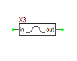
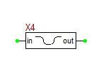
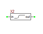
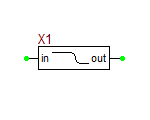
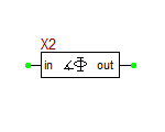
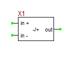
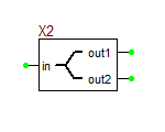
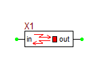
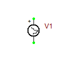
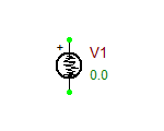
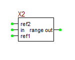
Difference between revisions of "Glossary of Black-Box Virtual Blocks"
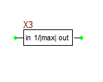
Kazem Sabet (Talk | contribs) |
Kazem Sabet (Talk | contribs) |
||
| Line 82: | Line 82: | ||
|- | |- | ||
|out_high||output high voltage level||V||5|| | |out_high||output high voltage level||V||5|| | ||
| + | |- | ||
| + | |} | ||
| + | |||
| + | == Amplitude Modulator Block== | ||
| + | |||
| + | [[File:GL87.png]] | ||
| + | |||
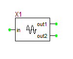
| + | This device takes an input signal and generates an AM modulated output signal of a specified carrier frequency with a specified modulation index. | ||
| + | |||
| + | Parameters: | ||
| + | |||
| + | {| class="wikitable" | ||
| + | |- | ||
| + | !NAME!!PARAMETER!!UNITS!!DEFAULT!!NOTES | ||
| + | |- | ||
| + | |r_in||input resistance||Ω||1G|| | ||
| + | |- | ||
| + | |r_out||output resistance||Ω||1u|| | ||
| + | |- | ||
| + | |m||modulation index||-||0.5|| | ||
| + | |- | ||
| + | |fc||carrier frequency||Hz||1Meg|| | ||
| + | |- | ||
| + | |ac||carrier peak amplitude||V||1|| | ||
| + | |- | ||
| + | |} | ||
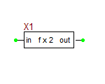
| + | |||
| + | == Amplitude Shift-Keying Modulator Block== | ||
| + | |||
| + | [[File:GL91.png]] | ||
| + | |||
| + | This device takes a digital input like a binary sequence and generates an ASK modulated output signal with two specified carrier amplitude levels. | ||
| + | |||
| + | Parameters: | ||
| + | |||
| + | {| class="wikitable" | ||
| + | |- | ||
| + | !NAME!!PARAMETER!!UNITS!!DEFAULT!!NOTES | ||
| + | |- | ||
| + | |r_out||output resistance||Ω||1u|| | ||
| + | |- | ||
| + | |fc||carrier frequency||Hz||1Meg|| | ||
| + | |- | ||
| + | |ac_lo||low carrier peak amplitude||V||0.0|| | ||
| + | |- | ||
| + | |ac_hi||high carrier peak amplitude||V||1.0|| | ||
|- | |- | ||
|} | |} | ||
| Line 122: | Line 168: | ||
|- | |- | ||
|fmax||maximum signal frequency||Hz||1Meg|| | |fmax||maximum signal frequency||Hz||1Meg|| | ||
| + | |- | ||
| + | |} | ||
| + | |||
| + | == Analog One-Half Frequency Divider Block== | ||
| + | |||
| + | [[File:GL78.png]] | ||
| + | |||
| + | This device takes a harmonic input signal and generates a harmonic output signal with a frequency one half lower and a user specified amplitude. | ||
| + | |||
| + | Parameters: | ||
| + | |||
| + | {| class="wikitable" | ||
| + | |- | ||
| + | !NAME!!PARAMETER!!UNITS!!DEFAULT!!NOTES | ||
| + | |- | ||
| + | |r_in||input resistance||Ω||1G|| | ||
| + | |- | ||
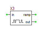
| + | |r_out||output resistance||Ω||1u|| | ||
| + | |- | ||
| + | |max_val||output amplitude||V||1.0|| | ||
| + | |- | ||
| + | |} | ||
| + | |||
| + | == Analog Phase-Locked Loop Block== | ||
| + | |||
| + | [[File:GL86.png]] | ||
| + | |||
| + | This 5-pin device is a parameterized model of an analog phase-locked loop. It provides two phase-locked output signals with square wave and triangular wave waveforms. The outputs of the lowpass filter and phase detector are also accessible via the designated pins. | ||
| + | |||
| + | Parameters: | ||
| + | |||
| + | {| class="wikitable" | ||
| + | |- | ||
| + | !NAME!!PARAMETER!!UNITS!!DEFAULT!!NOTES | ||
| + | |- | ||
| + | |r_in||input resistance||Ω||1G|| | ||
| + | |- | ||
| + | |r_out||output resistance||Ω||1u|| | ||
| + | |- | ||
| + | |K_d||voltage conversion factor of phase detector||V/rad||1.0|| | ||
| + | |- | ||
| + | |K_f||frequency conversion factor of VCO||Hz/V||1k|| | ||
| + | |- | ||
| + | |V_sq||square wave output peak amplitude||V||1|| | ||
| + | |- | ||
| + | |V_tri||triangular wave output peak amplitude||V||1|| | ||
| + | |- | ||
| + | |VT||VCO input dynamic range||V||1|| | ||
| + | |- | ||
| + | |r_time||VCO timing resistor||Ω||12k|| | ||
| + | |- | ||
| + | |c_time||VCO timing capacitor||F||10n|| | ||
| + | |- | ||
| + | |fo||VCO free-running frequency||Hz||1k|| | ||
| + | |- | ||
| + | |r_lpf||lowpass filter resistor||Ω||10k|| | ||
| + | |- | ||
| + | |c_lpf||lowpass filter capacitor||F||100n|| | ||
|- | |- | ||
|} | |} | ||
| Line 336: | Line 440: | ||
|- | |- | ||
|r_out_domain||output resistance smoothing domain||Ω||1n|| | |r_out_domain||output resistance smoothing domain||Ω||1n|| | ||
| + | |- | ||
| + | |} | ||
| + | |||
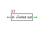
| + | == Delta Modulator Block== | ||
| + | |||
| + | [[File:GL95.png]] | ||
| + | |||
| + | This device samples an input signal at the specified sampling period and generates a Delta modulated output signal from it. | ||
| + | |||
| + | Parameters: | ||
| + | |||
| + | {| class="wikitable" | ||
| + | |- | ||
| + | !NAME!!PARAMETER!!UNITS!!DEFAULT!!NOTES | ||
| + | |- | ||
| + | |r_in||input resistance||Ω||1G|| | ||
| + | |- | ||
| + | |r_out||output resistance||Ω||1u|| | ||
| + | |- | ||
| + | |T||sampling period||sec||1|| | ||
| + | |- | ||
| + | |duty_cycle||sampling pulse duty cycle||-||0.01|| | ||
| + | |- | ||
| + | |} | ||
| + | |||
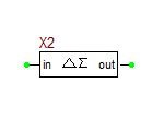
| + | == Delta-Sigma Modulator Block== | ||
| + | |||
| + | [[File:GL96.png]] | ||
| + | |||
| + | This device samples an input signal at the specified sampling period and generates a Delta-Sigma modulated output signal from it. | ||
| + | |||
| + | Parameters: | ||
| + | |||
| + | {| class="wikitable" | ||
| + | |- | ||
| + | !NAME!!PARAMETER!!UNITS!!DEFAULT!!NOTES | ||
| + | |- | ||
| + | |r_in||input resistance||Ω||1G|| | ||
| + | |- | ||
| + | |r_out||output resistance||Ω||1u|| | ||
| + | |- | ||
| + | |T||sampling period||sec||1|| | ||
| + | |- | ||
| + | |duty_cycle||sampling pulse duty cycle||-||0.01|| | ||
| + | |- | ||
| + | |} | ||
| + | |||
| + | == Differential Phase Shift-Keying Modulator Block== | ||
| + | |||
| + | [[File:GL94.png]] | ||
| + | |||
| + | This device takes a digital input like a binary sequence and generates a DPSK modulated output signal with two specified carrier phase values. It also requires a digital clock input for synchronization. | ||
| + | |||
| + | Parameters: | ||
| + | |||
| + | {| class="wikitable" | ||
| + | |- | ||
| + | !NAME!!PARAMETER!!UNITS!!DEFAULT!!NOTES | ||
| + | |- | ||
| + | |r_out||output resistance||Ω||1u|| | ||
| + | |- | ||
| + | |phi_lo||low carrier phase value||rad||0|| | ||
| + | |- | ||
| + | |phi_hi||high carrier phase value||rad||π|| | ||
| + | |- | ||
| + | |fc||carrier frequency||Hz||1Meg|| | ||
| + | |- | ||
| + | |ac||carrier peak amplitude||V||1.0|| | ||
|- | |- | ||
|} | |} | ||
| Line 653: | Line 825: | ||
|- | |- | ||
|max_in||input amplitude||V||1|| | |max_in||input amplitude||V||1|| | ||
| + | |- | ||
| + | |} | ||
| + | |||
| + | ==Frequency Doubler Block== | ||
| + | |||
| + | [[File:GL76.png]] | ||
| + | |||
| + | This device takes a harmonic input signal and generates a harmonic output signal with twice the frequency and a user specified amplitude. | ||
| + | |||
| + | Parameters: | ||
| + | |||
| + | {| class="wikitable" | ||
| + | |- | ||
| + | !NAME!!PARAMETER!!UNITS!!DEFAULT!!NOTES | ||
| + | |- | ||
| + | |r_in||input resistance||Ω||1G|| | ||
| + | |- | ||
| + | |r_out||output resistance||Ω||1u|| | ||
| + | |- | ||
| + | |max_val||output amplitude||V||1.0|| | ||
| + | |- | ||
| + | |} | ||
| + | |||
| + | == Frequency Down-Converter Block== | ||
| + | |||
| + | [[File:GL80.png]] | ||
| + | |||
| + | This 3-pin device takes two harmonic input signals with different frequencies f<sub>LO</sub> and f<sub>IF</sub> and generates a harmonic output signal with a frequency equal to f<sub>RF</sub> = f<sub>LO</sub> - f<sub>IF</sub> and a user specified amplitude. | ||
| + | |||
| + | Parameters: | ||
| + | |||
| + | {| class="wikitable" | ||
| + | |- | ||
| + | !NAME!!PARAMETER!!UNITS!!DEFAULT!!NOTES | ||
| + | |- | ||
| + | |r_in||input resistance||Ω||1G|| | ||
| + | |- | ||
| + | |r_out||output resistance||Ω||1u|| | ||
| + | |- | ||
| + | |max_in||peak amplitude of both inputs||V||1.0||Both inputs must have equal amplitudes. | ||
| + | |- | ||
| + | |max_out||output amplitude||V||1.0|| | ||
| + | |- | ||
| + | |} | ||
| + | |||
| + | == Frequency Modulator Block== | ||
| + | |||
| + | [[File:GL88.png]] | ||
| + | |||
| + | This device takes an input signal and generates an FM modulated output signal of a specified carrier frequency with a specified maximum frequency deviation. | ||
| + | |||
| + | Parameters: | ||
| + | |||
| + | {| class="wikitable" | ||
| + | |- | ||
| + | !NAME!!PARAMETER!!UNITS!!DEFAULT!!NOTES | ||
| + | |- | ||
| + | |r_in||input resistance||Ω||1G|| | ||
| + | |- | ||
| + | |r_out||output resistance||Ω||1u|| | ||
| + | |- | ||
| + | |f_del||maximum frequency deviation||Hz||500k|| | ||
| + | |- | ||
| + | |fc||carrier frequency||Hz||1Meg|| | ||
| + | |- | ||
| + | |ac||carrier peak amplitude||V||1|| | ||
| + | |- | ||
| + | |} | ||
| + | |||
| + | == Frequency Shift-Keying Modulator Block== | ||
| + | |||
| + | [[File:GL92.png]] | ||
| + | |||
| + | This device takes a digital input like a binary sequence and generates an FSK modulated output signal with two specified carrier frequencies. | ||
| + | |||
| + | Parameters: | ||
| + | |||
| + | {| class="wikitable" | ||
| + | |- | ||
| + | !NAME!!PARAMETER!!UNITS!!DEFAULT!!NOTES | ||
| + | |- | ||
| + | |r_out||output resistance||Ω||1u|| | ||
| + | |- | ||
| + | |fc_lo||low carrier frequency||Hz||1Meg|| | ||
| + | |- | ||
| + | |fc_hi||high carrier frequency||Hz||2Meg|| | ||
| + | |- | ||
| + | |ac||carrier peak amplitude||V||1.0|| | ||
| + | |- | ||
| + | |} | ||
| + | |||
| + | == Frequency Up-Converter Block== | ||
| + | |||
| + | [[File:GL79.png]] | ||
| + | |||
| + | This 3-pin device takes two harmonic input signals with different frequencies f<sub>LO</sub> and f<sub>IF</sub> and generates a harmonic output signal with a frequency equal to f<sub>RF</sub> = f<sub>LO</sub> + f<sub>IF</sub> and a user specified amplitude. | ||
| + | |||
| + | Parameters: | ||
| + | |||
| + | {| class="wikitable" | ||
| + | |- | ||
| + | !NAME!!PARAMETER!!UNITS!!DEFAULT!!NOTES | ||
| + | |- | ||
| + | |r_in||input resistance||Ω||1G|| | ||
| + | |- | ||
| + | |r_out||output resistance||Ω||1u|| | ||
| + | |- | ||
| + | |max_in||peak amplitude of both inputs||V||1.0||both inputs must have equal amplitudes. | ||
| + | |- | ||
| + | |max_out||output amplitude||V||1.0|| | ||
|- | |- | ||
|} | |} | ||
| Line 689: | Line 971: | ||
|- | |- | ||
|out_offset||out_offset||V||0.0|| | |out_offset||out_offset||V||0.0|| | ||
| + | |- | ||
| + | |} | ||
| + | |||
| + | ==Generalized Analog Filter Block== | ||
| + | |||
| + | [[File:GL85.png]] | ||
| + | |||
| + | This block models a generalize analog filter characterized by a rational transfer functions in the spectral domain Laplace variable s: | ||
| + | |||
| + | <math> H(s) = \frac{N(s)}{D(s)} = \frac{ \sum_{m=0}^{M} b_m s^m }{ \sum_{n=0}^{N} a_n s^n } </math> | ||
| + | |||
| + | subject to the requirement N ≥ M and a<sub>N</sub> = 1. To access the parameters of this block, you have to click the {{key|Edit Model...}} button of its property dialog. | ||
| + | |||
| + | The functionality of this block, which is native to [[RF.Spice A/D]], is very similar to the s-domain transfer function block, which is an XPSICE process model. This block does not have a denormalization frequency parameter. Therefore, at frequencies other than the unit frequency, the transfer function must be explicitly scaled. This block can be used in conjunction with both transient and AC frequency sweep tests. | ||
| + | |||
| + | Parameters: | ||
| + | |||
| + | {| class="wikitable" | ||
| + | |- | ||
| + | !NAME!!PARAMETER!!UNITS!!DEFAULT!!NOTES | ||
| + | |- | ||
| + | |deg||highest degree of s in transfer function||-||2||required | ||
| + | |- | ||
| + | |coeff_den||denominator coefficients array: coefficients of powers of s, highest power first||-||1 0 1||required | ||
| + | |- | ||
| + | |coeff_num||numerator coefficients array: coefficients of powers of s, highest power first||-||0 0 1||required | ||
| + | |- | ||
| + | |r_in||input resistance||Ω||10G|| | ||
| + | |- | ||
| + | |r_out||output resistance||Ω||1u|| | ||
|- | |- | ||
|} | |} | ||
| Line 715: | Line 1,027: | ||
|- | |- | ||
|freq||sampling frequency||Hz||1||required | |freq||sampling frequency||Hz||1||required | ||
| + | |- | ||
| + | |} | ||
| + | |||
| + | == Generic Bandpass Filter Block== | ||
| + | |||
| + | [[File:GL83.png]] | ||
| + | |||
| + | This device is a generic bandpass filter with user specified center frequency and bandwidth. It is based on a fifth-order Butterworth LC ladder topology. | ||
| + | |||
| + | Parameters: | ||
| + | |||
| + | {| class="wikitable" | ||
| + | |- | ||
| + | !NAME!!PARAMETER!!UNITS!!DEFAULT!!NOTES | ||
| + | |- | ||
| + | |f0||center frequency||Hz||1Meg|| | ||
| + | |- | ||
| + | |bw||bandwidth||Hz||200k|| | ||
| + | |- | ||
| + | |r0||source/load resistance||Ω||50|| | ||
| + | |- | ||
| + | |} | ||
| + | |||
| + | == Generic Bandstop Filter Block== | ||
| + | |||
| + | [[File:GL84.png]] | ||
| + | |||
| + | This device is a generic bandstop filter with user specified center frequency and bandwidth. It is based on a fifth-order Butterworth LC ladder topology. | ||
| + | |||
| + | Parameters: | ||
| + | |||
| + | {| class="wikitable" | ||
| + | |- | ||
| + | !NAME!!PARAMETER!!UNITS!!DEFAULT!!NOTES | ||
| + | |- | ||
| + | |f0||center frequency||Hz||1Meg|| | ||
| + | |- | ||
| + | |bw||bandwidth||Hz||200k|| | ||
| + | |- | ||
| + | |r0||source/load resistance||Ω||50|| | ||
| + | |- | ||
| + | |} | ||
| + | |||
| + | == Generic Highpass Filter Block== | ||
| + | |||
| + | [[File:GL82.png]] | ||
| + | |||
| + | This device is a generic highpass filter with a user specified cutoff frequency. It is based on a fifth-order Butterworth LC ladder topology. | ||
| + | |||
| + | Parameters: | ||
| + | |||
| + | {| class="wikitable" | ||
| + | |- | ||
| + | !NAME!!PARAMETER!!UNITS!!DEFAULT!!NOTES | ||
| + | |- | ||
| + | |cutoff||cutoff frequency||Hz||1Meg|| | ||
| + | |- | ||
| + | |r0||source/load resistance||Ω||50|| | ||
| + | |- | ||
| + | |} | ||
| + | |||
| + | == Generic Lowpass Filter Block== | ||
| + | [[File:GL81.png]] | ||
| + | |||
| + | This device is a generic lowpass filter with a user specified cutoff frequency. It is based on a fifth-order Butterworth LC ladder topology. | ||
| + | |||
| + | [[Parameters]]: | ||
| + | |||
| + | {| class="wikitable" | ||
| + | |- | ||
| + | !NAME!!PARAMETER!!UNITS!!DEFAULT!!NOTES | ||
| + | |- | ||
| + | |cutoff||cutoff frequency||Hz||1Meg|| | ||
| + | |- | ||
| + | |r0||source/load resistance||Ω||50|| | ||
|- | |- | ||
|} | |} | ||
| Line 1,244: | Line 1,631: | ||
|- | |- | ||
|K_v||voltage conversion factor||V/rad||1|| | |K_v||voltage conversion factor||V/rad||1|| | ||
| + | |- | ||
| + | |} | ||
| + | |||
| + | == Phase Modulator Block== | ||
| + | |||
| + | [[File:GL89.png]] | ||
| + | |||
| + | This device takes an input signal and generates an PM modulated output signal of a specified carrier frequency with a specified maximum phase deviation. | ||
| + | |||
| + | Parameters: | ||
| + | |||
| + | {| class="wikitable" | ||
| + | |- | ||
| + | !NAME!!PARAMETER!!UNITS!!DEFAULT!!NOTES | ||
| + | |- | ||
| + | |r_in||input resistance||Ω||1G|| | ||
| + | |- | ||
| + | |r_out||output resistance||Ω||1u|| | ||
| + | |- | ||
| + | |phi_del||maximum phase deviation||rad||π|| | ||
| + | |- | ||
| + | |fc||carrier frequency||Hz||1Meg|| | ||
| + | |- | ||
| + | |ac||carrier peak amplitude||V||1|| | ||
| + | |- | ||
| + | |phi0||carrier phase||rad||0|| | ||
| + | |- | ||
| + | |} | ||
| + | |||
| + | == Phase Shift-Keying Modulator Block== | ||
| + | |||
| + | [[File:GL93.png]] | ||
| + | |||
| + | This device takes a digital input like a binary sequence and generates a PSK modulated output signal with two specified carrier phase values. | ||
| + | |||
| + | Parameters: | ||
| + | |||
| + | {| class="wikitable" | ||
| + | |- | ||
| + | !NAME!!PARAMETER!!UNITS!!DEFAULT!!NOTES | ||
| + | |- | ||
| + | |r_out||output resistance||Ω||1u|| | ||
| + | |- | ||
| + | |phi_lo||low carrier phase value||rad||0|| | ||
| + | |- | ||
| + | |phi_hi||high carrier phase value||rad||π|| | ||
| + | |- | ||
| + | |fc||carrier frequency||Hz||1Meg|| | ||
| + | |- | ||
| + | |ac||carrier peak amplitude||V||1.0|| | ||
|- | |- | ||
|} | |} | ||
| Line 1,320: | Line 1,757: | ||
|-|- | |-|- | ||
|out_high||high output voltage level||V||+1|| | |out_high||high output voltage level||V||+1|| | ||
| + | |- | ||
| + | |} | ||
| + | |||
| + | == Pulse Width Modulator Block== | ||
| + | |||
| + | [[File:GL97.png]] | ||
| + | |||
| + | This device takes an input signal and compares it to an internally generated ramp signal with a specified period and generates a binary PWM modulated output signal. A designated pin provides the ramp signal output. | ||
| + | |||
| + | Parameters: | ||
| + | |||
| + | {| class="wikitable" | ||
| + | |- | ||
| + | !NAME!!PARAMETER!!UNITS!!DEFAULT!!NOTES | ||
| + | |- | ||
| + | |r_in||input resistance||Ω||1G|| | ||
| + | |- | ||
| + | |r_out||output resistance||Ω||1u|| | ||
| + | |- | ||
| + | |V_lo||low output voltage level||V||0|| | ||
| + | |- | ||
| + | |V_hi||high output voltage level||V||1|| | ||
| + | |- | ||
| + | |V_lo||hysteresis voltage tolerance||V||100m|| | ||
| + | |- | ||
| + | |T_rmp||sampling period||sec||1m|| | ||
| + | |- | ||
| + | |rmp_lo||ramp minimum voltage level||V||0|| | ||
| + | |- | ||
| + | |rmp_hi||ramp maximum voltage level||V||1|| | ||
| + | |- | ||
| + | |duty_cycle||ramp duty cycle||-||0.01||Must be between 0.01 and 0.99 | ||
| + | |- | ||
| + | |} | ||
| + | |||
| + | == Quadrature Amplitude Modulator Block== | ||
| + | |||
| + | [[File:GL90.png]] | ||
| + | |||
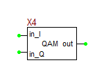
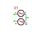
| + | This 3-pin device takes two input signals and generates a QAM modulated output signal of a specified carrier frequency: | ||
| + | |||
| + | <math> v_{out}(t) = A_c \left( v_{in_I}(t) \cdot \cos(2\pi f_c t) + v_{in_Q}(t) \cdot \sin(2\pi f_c t) \right) </math> | ||
| + | |||
| + | Parameters: | ||
| + | |||
| + | {| class="wikitable" | ||
| + | |- | ||
| + | !NAME!!PARAMETER!!UNITS!!DEFAULT!!NOTES | ||
| + | |- | ||
| + | |r_in||input resistance||Ω||1G|| | ||
| + | |- | ||
| + | |r_out||output resistance||Ω||1u|| | ||
| + | |- | ||
| + | |fc||carrier frequency||Hz||1Meg|| | ||
| + | |- | ||
| + | |ac||carrier peak amplitude||V||1|| | ||
|- | |- | ||
|} | |} | ||
| Line 1,684: | Line 2,177: | ||
|- | |- | ||
|chirp_type||0 for up-chirp, 1 for down-chirp||-||0|| | |chirp_type||0 for up-chirp, 1 for down-chirp||-||0|| | ||
| + | |- | ||
| + | |} | ||
| + | |||
| + | ==Sine Wave VCO Block== | ||
| + | |||
| + | [[File:GL73.png]] | ||
| + | |||
| + | This device is a voltage-controlled oscillator block with a sinusoidal output signal. | ||
| + | |||
| + | Parameters: | ||
| + | |||
| + | {| class="wikitable" | ||
| + | |- | ||
| + | !NAME!!PARAMETER!!UNITS!!DEFAULT!!NOTES | ||
| + | |- | ||
| + | |fo||free-running frequency||Hz||1Meg|| | ||
| + | |- | ||
| + | |K_f||frequency conversion factor||Hz/V||500k|| | ||
| + | |- | ||
| + | |max_val||output peak amplitude||V||1|| | ||
|- | |- | ||
|} | |} | ||
| Line 1,772: | Line 2,285: | ||
|- | |- | ||
|chirp_type||0 for up-chirp, 1 for down-chirp||-||0|| | |chirp_type||0 for up-chirp, 1 for down-chirp||-||0|| | ||
| + | |- | ||
| + | |} | ||
| + | |||
| + | ==Square Wave VCO Block== | ||
| + | |||
| + | [[File:GL75.png]] | ||
| + | |||
| + | This device is a voltage-controlled oscillator block with a square wave output signal oscillating between two binary voltage levels. | ||
| + | |||
| + | Parameters: | ||
| + | |||
| + | {| class="wikitable" | ||
| + | |- | ||
| + | !NAME!!PARAMETER!!UNITS!!DEFAULT!!NOTES | ||
| + | |- | ||
| + | |fo||free-running frequency||Hz||1Meg|| | ||
| + | |- | ||
| + | |K_f||frequency conversion factor||Hz/V||500k|| | ||
| + | |- | ||
| + | |duty_cycle||pulse duty cycle||-||0.5|| | ||
| + | |- | ||
| + | |rise_time||pulse rise time||sec||1n|| | ||
| + | |- | ||
| + | |fall_time||pulse fall time||sec||1n|| | ||
| + | |- | ||
| + | |out_low||output lower limit||V||-1.0|| | ||
| + | |- | ||
| + | |out_high||output higher limit||V||-1.0|| | ||
|- | |- | ||
|} | |} | ||
| Line 1,930: | Line 2,471: | ||
|- | |- | ||
|max_val||maximum output voltage level||V||1|| | |max_val||maximum output voltage level||V||1|| | ||
| + | |- | ||
| + | |} | ||
| + | |||
| + | ==Triangular Wave VCO Block== | ||
| + | |||
| + | [[File:GL74.png]] | ||
| + | |||
| + | This device is a voltage-controlled oscillator block with a triangular wave output signal oscillating between two binary voltage levels. The parameter "duty_cycle" has a default value of 0.5, generating a symmetric triangular output. In the limiting cases of duty_cycle = 0.99 and duty_cycle = 0.01, the output will have an up-ramp or a down-ramp sawtooth waveform, respectively. | ||
| + | |||
| + | Parameters: | ||
| + | |||
| + | {| class="wikitable" | ||
| + | |- | ||
| + | !NAME!!PARAMETER!!UNITS!!DEFAULT!!NOTES | ||
| + | |- | ||
| + | |fo||free-running frequency||Hz||1Meg|| | ||
| + | |- | ||
| + | |K_f||frequency conversion factor||Hz/V||500k|| | ||
| + | |- | ||
| + | |duty_cycle||triangular waveform duty cycle||-||0.5||Must be between 0.01 and 0.99. | ||
| + | |- | ||
| + | |out_low||output lower limit||V||-1.0|| | ||
| + | |- | ||
| + | |out_high||output higher limit||V||-1.0|| | ||
| + | |- | ||
| + | |} | ||
| + | |||
| + | == xN Frequency Multiplier Block== | ||
| + | |||
| + | [[File:GL77.png]] | ||
| + | |||
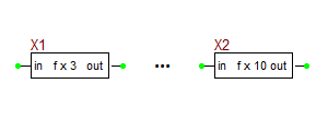
| + | These devices take a harmonic input signal and generate a harmonic output signal with a frequency N times larger and a user specified amplitude: N = 3, 4, 5, 6, 7, 8, 9, 10. | ||
| + | |||
| + | Parameters: | ||
| + | |||
| + | {| class="wikitable" | ||
| + | |- | ||
| + | !NAME!!PARAMETER!!UNITS!!DEFAULT!!NOTES | ||
| + | |- | ||
| + | |r_in||input resistance||Ω||1G|| | ||
| + | |- | ||
| + | |r_out||output resistance||Ω||1u|| | ||
| + | |- | ||
| + | |max_val||output amplitude||V||1.0|| | ||
|- | |- | ||
|} | |} | ||
Latest revision as of 17:10, 8 November 2016
Contents
- 1 4-Bit A/D Converter Block
- 2 4-Bit D/A Converter Block
- 3 4-Bit Signal Digitizer Block
- 4 8-Bit A/D Converter Block
- 5 8-Bit D/A Converter Block
- 6 Amplitude Modulator Block
- 7 Amplitude Shift-Keying Modulator Block
- 8 Analog Differentiator Block
- 9 Analog integrator Block
- 10 Analog One-Half Frequency Divider Block
- 11 Analog Phase-Locked Loop Block
- 12 Arithmetic Mean Block
- 13 Clocked Sample-and-Hold Block
- 14 Comparator with Hysteresis
- 15 Complex Modulus Block
- 16 Controlled Limiter Block
- 17 Controlled One-Shot
- 18 Current Limiter Block
- 19 Delta Modulator Block
- 20 Delta-Sigma Modulator Block
- 21 Differential Phase Shift-Keying Modulator Block
- 22 Differentiator Block
- 23 Digital Integrator Block
- 24 Discrete Convolution Block
- 25 Discrete Fourier Transform (DFT) Block
- 26 Discrete-Time Fourier Transform (DTFT) Block
- 27 Discrete-Time Signal Hold Block
- 28 Divider Block
- 29 Finite Sequence Pulse Generator
- 30 Finite Sequence Random Pulse Generator
- 31 Finite Sequence Signal Sampler Block
- 32 Frequency Detector Block
- 33 Frequency Doubler Block
- 34 Frequency Down-Converter Block
- 35 Frequency Modulator Block
- 36 Frequency Shift-Keying Modulator Block
- 37 Frequency Up-Converter Block
- 38 Gain Block
- 39 Generalized Analog Filter Block
- 40 Generalized Digital Filter Block
- 41 Generic Bandpass Filter Block
- 42 Generic Bandstop Filter Block
- 43 Generic Highpass Filter Block
- 44 Generic Lowpass Filter Block
- 45 Geometric Mean Block
- 46 Gudermannian Polarity Detector Block
- 47 Ideal Buffer Block
- 48 Ideal Comparator Block
- 49 Ideal Delay Block
- 50 Ideal Full-Wave Rectifier Block
- 51 Ideal Gyrator Block
- 52 Ideal Half-Wave Rectifier Block
- 53 Ideal Phase Shifter Block
- 54 Ideal Polarity Detector Block
- 55 Ideal Splitter Block
- 56 Impulse Generator
- 57 Integer Modulo Block
- 58 Integrator Block
- 59 Leading Edge Detector Block
- 60 Limiter Block
- 61 Link Propagation Block
- 62 Maximum Detector Block
- 63 Maximum Selector Block
- 64 Minimum Detector Block
- 65 Minimum Selector Block
- 66 Multiplier Block
- 67 One-Shot Sample-and-Hold Block
- 68 Peak Detector Block
- 69 Phase Detector Block
- 70 Phase Modulator Block
- 71 Phase Shift-Keying Modulator Block
- 72 Piecewise Linear Map Block
- 73 Polar-to-Rect Coordinates Conversion Block
- 74 Pulse Generator
- 75 Pulse Width Modulator Block
- 76 Quadrature Amplitude Modulator Block
- 77 Quadrature Harmonic Wave Generator
- 78 Radar Echo Block
- 79 Ramp Generator
- 80 Random Digitized Signal Generator
- 81 Random Noise Generator
- 82 Random Pulse Generator
- 83 Range-Crossing Detector Block
- 84 Rect-to-Polar Coordinates Conversion Block
- 85 S-Domain Transfer Function Block
- 86 Schmitt Trigger Block
- 87 Sigmoid Polarity Detector Block
- 88 Signal Normalizer Block
- 89 Signal Sampler Block
- 90 Sine-to-Square Wave Converter Block
- 91 Sine Wave Chirp Generator
- 92 Sine Wave VCO Block
- 93 Slew Rate Block
- 94 Slope Detector Block
- 95 Square Wave Chirp Generator
- 96 Square Wave VCO Block
- 97 Summer Block
- 98 Temporal Window Block
- 99 Trailing Edge Detector Block
- 100 Triangular-to-Sine Wave Converter Block
- 101 Triangular-to-Square Wave Converter Block
- 102 Triangular Wave Chirp Generator
- 103 Triangular Wave Generator
- 104 Triangular Wave VCO Block
- 105 xN Frequency Multiplier Block
- 106 Zero-Crossing Detector Block
4-Bit A/D Converter Block
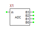
This is a 5-pin mixed-signal device with an analog input and 4 digital outputs. Based on the specified maximum input voltage level, a total of 16 discrete voltage levels are established. The block fits the input analog voltage between two of these 16 discrete levels and outputs the 4-bit binary equivalent to 4 digital pins B0-B3 representing the LSB and MSB, respectively.
Parameters:
| NAME | PARAMETER | UNITS | DEFAULT | NOTES |
|---|---|---|---|---|
| max_val | maximum input voltage | V | 5 |
4-Bit D/A Converter Block
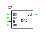
This is a 5-pin mixed-signal device with 4 digital inputs and an analog output. Based on the specified low and high output voltage levels, a total of 16 discrete voltage levels are established. The block converts the input 4-bit word (B0-B3 representing the LSB and MSB, respectively) to the corresponding discrete voltage level and outputs it as an analog voltage signal.
Parameters:
| NAME | PARAMETER | UNITS | DEFAULT | NOTES |
|---|---|---|---|---|
| out_low | output low voltage level | V | 0 | |
| out_high | output high voltage level | V | 5 |
4-Bit Signal Digitizer Block
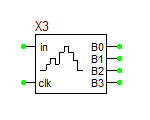
This is a 6-pin mixed-signal device with an analog input, a digital clock and 4 digital outputs. It samples its analog input signal at the period of the supplied digital clock. The digitized version of the input signal is sent out to 4 digital outputs B0-B3 representing the LSB and MSB, respectively.
Parameters:
| NAME | PARAMETER | UNITS | DEFAULT | NOTES |
|---|---|---|---|---|
| r_in | input resistance | Ω | 10G | |
| max_val | maximum input voltage | V | 5 |
8-Bit A/D Converter Block
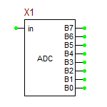
This is a 9-pin mixed-signal device with an analog input and 8 digital outputs. Based on the specified maximum input voltage level, a total of 256 discrete voltage levels are established. The block fits the input analog voltage between two of these 256 discrete levels and outputs the 8-bit binary equivalent to 8 digital pins B0-B7 representing the LSB and MSB, respectively.
Parameters:
| NAME | PARAMETER | UNITS | DEFAULT | NOTES |
|---|---|---|---|---|
| max_val | maximum input voltage | V | 5 |
8-Bit D/A Converter Block
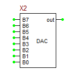
This is a 9-pin mixed-signal device with 8 digital inputs and an analog output. Based on the specified low and high output voltage levels, a total of 256 discrete voltage levels are established. The block converts the input 8-bit word (B0-B7 representing the LSB and MSB, respectively) to the corresponding discrete voltage level and outputs it as an analog voltage signal.
Parameters:
| NAME | PARAMETER | UNITS | DEFAULT | NOTES |
|---|---|---|---|---|
| out_low | output low voltage level | V | 0 | |
| out_high | output high voltage level | V | 5 |
Amplitude Modulator Block
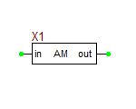
This device takes an input signal and generates an AM modulated output signal of a specified carrier frequency with a specified modulation index.
Parameters:
| NAME | PARAMETER | UNITS | DEFAULT | NOTES |
|---|---|---|---|---|
| r_in | input resistance | Ω | 1G | |
| r_out | output resistance | Ω | 1u | |
| m | modulation index | - | 0.5 | |
| fc | carrier frequency | Hz | 1Meg | |
| ac | carrier peak amplitude | V | 1 |
Amplitude Shift-Keying Modulator Block
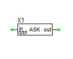
This device takes a digital input like a binary sequence and generates an ASK modulated output signal with two specified carrier amplitude levels.
Parameters:
| NAME | PARAMETER | UNITS | DEFAULT | NOTES |
|---|---|---|---|---|
| r_out | output resistance | Ω | 1u | |
| fc | carrier frequency | Hz | 1Meg | |
| ac_lo | low carrier peak amplitude | V | 0.0 | |
| ac_hi | high carrier peak amplitude | V | 1.0 |
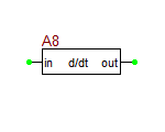
Analog Differentiator Block
This device outputs the derivative of its input signal. It is a native RF.Spice A/D block and different from the XSPICE Differentiator Block, which is a more extensive model.
Parameters:
| NAME | PARAMETER | UNITS | DEFAULT | NOTES |
|---|---|---|---|---|
| gain | gain | - | 1.0 | |
| offset | offset voltage | V | 0 | |
| fmax | maximum signal frequency | Hz | 1Meg |
Analog integrator Block
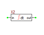
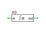
This device outputs the integral of its input signal assuming zero initial conditions. It is a native RF.Spice A/D block and different from the XSPICE Integrator Block, which is a more extensive model.
Parameters:
| NAME | PARAMETER | UNITS | DEFAULT | NOTES |
|---|---|---|---|---|
| gain | gain | - | 1.0 | |
| offset | offset voltage | V | 0 | |
| fmax | maximum signal frequency | Hz | 1Meg |
Analog One-Half Frequency Divider Block
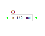
This device takes a harmonic input signal and generates a harmonic output signal with a frequency one half lower and a user specified amplitude.
Parameters:
| NAME | PARAMETER | UNITS | DEFAULT | NOTES |
|---|---|---|---|---|
| r_in | input resistance | Ω | 1G | |
| r_out | output resistance | Ω | 1u | |
| max_val | output amplitude | V | 1.0 |
Analog Phase-Locked Loop Block
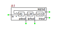
This 5-pin device is a parameterized model of an analog phase-locked loop. It provides two phase-locked output signals with square wave and triangular wave waveforms. The outputs of the lowpass filter and phase detector are also accessible via the designated pins.
Parameters:
| NAME | PARAMETER | UNITS | DEFAULT | NOTES |
|---|---|---|---|---|
| r_in | input resistance | Ω | 1G | |
| r_out | output resistance | Ω | 1u | |
| K_d | voltage conversion factor of phase detector | V/rad | 1.0 | |
| K_f | frequency conversion factor of VCO | Hz/V | 1k | |
| V_sq | square wave output peak amplitude | V | 1 | |
| V_tri | triangular wave output peak amplitude | V | 1 | |
| VT | VCO input dynamic range | V | 1 | |
| r_time | VCO timing resistor | Ω | 12k | |
| c_time | VCO timing capacitor | F | 10n | |
| fo | VCO free-running frequency | Hz | 1k | |
| r_lpf | lowpass filter resistor | Ω | 10k | |
| c_lpf | lowpass filter capacitor | F | 100n |
Arithmetic Mean Block
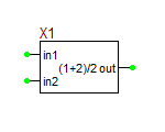
This 3-pin device sends the arithmetic mean or average of its two inputs to the output with a default unity gain.
Parameters:
| NAME | PARAMETER | UNITS | DEFAULT | NOTES |
|---|---|---|---|---|
| gain | gain | - | 1.0 |
Clocked Sample-and-Hold Block
This device samples its input signal at a specified sampling period and holds the values of each sample during each clock cycle. The output signal is a quantized version of the input signal.
Parameters:
| NAME | PARAMETER | UNITS | DEFAULT | NOTES |
|---|---|---|---|---|
| T | sampling period | sec | 1 | required |
| duty_cycle | sampling pulse duty cycle | - | 0.1 | |
| Tmax | signal period or maximum duration | sec | 10 |
Comparator with Hysteresis
This device is a 3-pin two-signal voltage comparator block with hysteresis effect. If the output voltage is at its low level and you increase Δv = (vpos - vneg), the output switches to the high level as soon as Δv > V_hys. If the output voltage is at its high level and you decrease Δv = (vpos - vneg), the output switches to the low level as soon as Δv < -V_hys.
Parameters:
| NAME | PARAMETER | UNITS | DEFAULT | NOTES |
|---|---|---|---|---|
| V_hi | high output voltage level | V | 5 | |
| V_lo | high output voltage level | v | 100m | |
| V_hys | hysteresis voltage width | V | 50m |
Complex Modulus Block
This 3-pin device assumes its first and second input signals to be the real and imaginary parts of a complex signal and sends the absolute value of such a complex signal to the output with a default unity gain.
Parameters:
| NAME | PARAMETER | UNITS | DEFAULT | NOTES |
|---|---|---|---|---|
| gain | gain | - | 1.0 |
Controlled Limiter Block
The Controlled Limiter is a single-input, single-output block similar to the Gain Block. However, the output of the Controlled Limiter function is restricted to the range specified by the output lower and upper limits. This model operates in DC, AC and Transient analysis modes. Note that the limit range is the value below the Upper Limit Control input signal (CNTL_UPPER) and above the Lower Limit Control input signal (CNTL_LOWER) at which smoothing of the output signal begins. A minimum positive value of voltage difference must exist between the CNTL_UPPER and CNTL_LOWER inputs at all times. The main difference between the Controlled Limiter Block and the Limiter Block is that the former's limits are set by input control voltages, while the latter's limits are set as numerical parameters.
Also note that the Controlled Limiter function examines the input values of CNTL_UPPER and CNTL_LOWER to make sure that they are spaced far enough apart to guarantee the existence of a linear range between them. The range is calculated as the difference between (cntl_upper - upper_delta - limit_range) and (cntl_lower + lower_delta + limit_range) and must be greater than or equal to zero. When the limit_range is specified as a fractional value, the limit_range used in the above is taken as the calculated fraction of the difference between cntl_upper and cntl_lower. Still, the potential exists for too great a limit_range value to be specified for proper operation, in which case the model will return an error message.
Model Identifier: climit
Netlist Format:
A<device_name> <in_pin> <cntl_upper_pin> <cntl_lower_pin> <out_pin> <model_name>
.model <model_name> climit {<param1 = value> < param2 = value> ...}
Example:
A1 1 2 3 4 controlled_limit_block
.model controlled_limit_block climit in_offset = 0.0 gain = 1.0 upper_delta = 0.0 lower_delta = 0.0
Parameters:
| NAME | PARAMETER | UNITS | DEFAULT | NOTES |
|---|---|---|---|---|
| in_offset | input offset | V | 0.0 | |
| gain | gain | - | 1.0 | |
| upper_delta | output upper delta | - | 0.0 | |
| lower_delta | output lower delta | - | 0.0 | |
| limit_range | upper and lower sm. Range | - | 1.0e-6 | |
| fraction | smoothing %/abs switch | - | False |
Controlled One-Shot
This is an eight-terminal function generator with a single pulse output. The pulse width is controlled by an input voltage. The functional dependency of the output pulse width on the input voltage is piecewise linear and is defined as a two-dimensional table similar to a piecewise linear (PWL) controlled source. In the "pulse width vs. voltage" curve, the array "cntl_array" defines voltage values in Volts and the array "pw_array" defines the corresponding pulse width values in seconds.
The generation of the output pulse is triggered either on the rising or falling edge of a clock input.
Model Identifier: oneshot
Netlist Format:
A<device_name> %vd(<clk_pin> <clk_ref_pin>) %vd(<cntl_in_pin> <cntl_in_ref_pin>) %vd(<clear_pin> <clear_ref_pin>) %vd(<out_pin> <out_ref_pin>) <model_name>
.model <model_name> oneshot {<param1 = value> < param2 = value> ...}
Example:
A1 %vd(1 5) %vd(2 6) %vd(3 7) %vd(4 8) one_shot
.model one_shot oneshot cntl_array = [0.0] pw_array = [1u] rise_time = 1n
Parameters:
| NAME | PARAMETER | UNIT | DEFAULT | NOTES |
|---|---|---|---|---|
| Clk_trig | clock trigger value | V | 0.5 | |
| Pos_edge_trig | positive/negative edge trigger switch | - | True | |
| Cntl_array | control array | V | [0.0] | required |
| Pw_array | pulse width array | sec | [1u] | required |
| Out_low | output low value | V | 0.0 | |
| Out_high | output high value | V | 1.0 | |
| Delay | output delay from trigger | sec | 1.0e-9 | |
| Rise_time | output rise time | sec | 1.0e-9 | |
| Fall_time | output fall time | sec | 1.0e-9 |
Current Limiter Block
The Current Limiter Block models the behavior of an operational amplifier or comparator device at a high level of abstraction. All of its pins act as inputs; three of the four also act as outputs. The model takes as input a voltage value from the “in” connector. It then applies an offset and a gain, and derives from it an equivalent internal voltage (veq), which it limits to fall between pos pwr and neg pwr. If veq is greater than the output voltage seen on the “out” connector, a sourcing current will flow from the output pin. Conversely, if the voltage is less than vout, a sinking current will flow into the output pin. Depending on the polarity of the current flow, either a sourcing or a sinking resistance value (r_out_source, r_out_sink) is applied to govern the vout/i_out relationship. The chosen resistance will continue to control the output current until it reaches a maximum value specified by either i_limit_source or i_limit_sink. The latter mimics the current limiting behavior of many operational amplifier output stages. During all operation, the output current is reflected either in the pos_pwr connector current or the neg_pwr current, depending on the polarity of i_out. Thus, realistic power consumption as seen in the supply rails is included in the model. The user-specified smoothing parameters relate to model operation as follows: v_pwr_range controls the voltage below vpos_pwr and above vneg_pwr inputs beyond which veq [= gain * (vin + voffset)] is smoothed; i_source_range specifies the current below i_limit_source at which smoothing begins, as well as specifying the current increment above i_out=0.0 at which i_pos_pwr begins to transition to zero; i_sink_range serves the same purpose with respect to i_limit_sink and i_neg_pwr that i_source_range serves for i_limit_source & i_pos_pwr; r_out_domain specifies the incremental value above and below (veq-vout)=0.0 at which r_out will be set to r_out_source and r_out_sink, respectively. For values of (veq-vout) less than r_out_domain and greater than -r_out_domain, r_out is interpolated smoothly between r_out_source & r_out_sink.
Model Identifier: ilimit
Netlist Format:
A<device_name> <in_pin> <pos_pwr_pin> <neg_pwr_pin> <out_pin> <model_name>
.model <model_name> ilimit {<param1 = value> < param2 = value> ...}
Example:
A1 1 2 3 4 amp
.model amp ilimit in_offset=0.0 gain=16.0 r_out_source=1.0 r_out_sink=1.0 i_limit_source=1e-3 i_limit_sink=10e-3 v_pwr_range=0.2 i_source_range=1e-6 i_sink_range=1e-6 r_out_domain=1e-6
Parameters:
| NAME | PARAMETER | UNITS | DEFAULT | NOTES |
|---|---|---|---|---|
| in_offset | input offset | V | 0.0 | |
| gain | gain | - | 1.0 | |
| r_out_source | sourcing resistance | Ω | 1.0 | |
| r_out_sink | sinking resistance | Ω | 1.0 | |
| i_limit_source | current sourcing limit | A | 10m | |
| i_limit_sink | current sinking limit | A | 10m | |
| v_pwr_range | power smoothing range | V | 1u | |
| i_source_range | current sourcing smoothing range | A | 1n | |
| i_sink_range | current sinking smoothing range | A | 1n | |
| r_out_domain | output resistance smoothing domain | Ω | 1n |
Delta Modulator Block
This device samples an input signal at the specified sampling period and generates a Delta modulated output signal from it.
Parameters:
| NAME | PARAMETER | UNITS | DEFAULT | NOTES |
|---|---|---|---|---|
| r_in | input resistance | Ω | 1G | |
| r_out | output resistance | Ω | 1u | |
| T | sampling period | sec | 1 | |
| duty_cycle | sampling pulse duty cycle | - | 0.01 |
Delta-Sigma Modulator Block
This device samples an input signal at the specified sampling period and generates a Delta-Sigma modulated output signal from it.
Parameters:
| NAME | PARAMETER | UNITS | DEFAULT | NOTES |
|---|---|---|---|---|
| r_in | input resistance | Ω | 1G | |
| r_out | output resistance | Ω | 1u | |
| T | sampling period | sec | 1 | |
| duty_cycle | sampling pulse duty cycle | - | 0.01 |
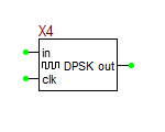
Differential Phase Shift-Keying Modulator Block
This device takes a digital input like a binary sequence and generates a DPSK modulated output signal with two specified carrier phase values. It also requires a digital clock input for synchronization.
Parameters:
| NAME | PARAMETER | UNITS | DEFAULT | NOTES |
|---|---|---|---|---|
| r_out | output resistance | Ω | 1u | |
| phi_lo | low carrier phase value | rad | 0 | |
| phi_hi | high carrier phase value | rad | π | |
| fc | carrier frequency | Hz | 1Meg | |
| ac | carrier peak amplitude | V | 1.0 |
Differentiator Block
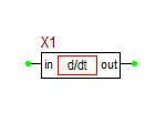
The Differentiator Block approximates the time derivative of an input signal by calculating the incremental slope of that signal since the previous time point. Gain and output offset parameters are also included to allow for tailoring of the required signal. Output upper and lower limits are also included to prevent convergence erros resulting from excessively large output values. The incremental value of output below the output_upper_limit and above the output_lower_limit at which smoothing begins is specified via the limit_range parameter. In AC analysis, the value returned is equal to the radian frequency of analysis multiplied by the gain.
Model Identifier: d_dt
Netlist Format:
A<device_name> <in_pin> <out_pin> <model_name>
.model <model_name> d_dt out_lower_limit = <value> out_upper_limit = <value> {<param1 = value> < param2 = value> ...}
Example:
A1 1 2 differentiator
.model differentiator d_dt out_lower_limit = -1t out_upper_limit = 1t
Parameters:
| NAME | PARAMETER | UNITS | DEFAULT | NOTES |
|---|---|---|---|---|
| gain | gain | - | 1.0 | |
| out_offset | output offset | V | 0.0 | |
| out_lower_limit | output lower limit | V | -1t | required |
| out_upper_limit | output upper limit | V | 1t | required |
| limit_range | upper and lower limit smoothing range | - | 1.0e-6 |
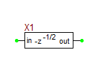
Digital Integrator Block
This device models a digital integrator with a Z-transform of -z-1/2, which is equivalent to a delay line with a delay of half the sampling period
Parameters:
| NAME | PARAMETER | UNITS | DEFAULT | NOTES |
|---|---|---|---|---|
| T | sampling period | sec | 1 | required |
Discrete Convolution Block
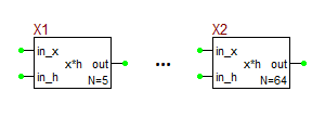
These blocks perform an N-point discrete convolution of their input signals. Both of the input signals x(t) and h(t) are sampled at the specified sampling period. The samples of x(t) are then shifted in time for the convolution. The output signal is a pulse train of the same period with the specified duty cycle. The input signal of these block can be either continuous-time signals or pulse trains of the specified period.
Parameters:
| NAME | PARAMETER | UNITS | DEFAULT | NOTES |
|---|---|---|---|---|
| T | sampling period | sec | 1 | required |
| rise_time | window rise time | sec | 0 | |
| fall_time | window fall time | sec | 0 | |
| duty_cycle | output pulse duty cycle | - | 0.1 | |
| gain | output gain | - | 1 |
Discrete Fourier Transform (DFT) Block
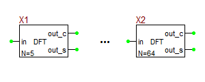
These blocks perform an M-point discrete Fourier transform (DFT) of their input signal and then sample each period of the Fourier transform N times in the frequency domain. The output signals are two finite sequence pulse trains representing the cosine and sine DFT transforms. The input signal of these block can be either a continuous-time signal or a pulse train of the specified period.
There are ten DFT blocks for M = 5, 6, 7, 8, 9, 10, 12, 16, 32, 64. In each case, the total duration of the transform window is MT, where T is the sampling period. By default, the frequency domain sampling starts at t = MT and takes place over one spectral period equal to fs = 1/T. You can change the sampling start time by "n_delay" temporal periods. n_delay = 0 by default, but it can be either positive or negative. You can also extend spectral sampling to more than one spectral period by increasing the value of the parameter "n_dur", which has a default value of 1.
Parameters:
| NAME | PARAMETER | UNITS | DEFAULT | NOTES |
|---|---|---|---|---|
| T | sampling period | sec | 1 | required |
| N | sequence length | - | 5 | required |
| rise_time | window rise time | sec | 0 | |
| fall_time | window fall time | sec | 0 | |
| duty_cycle | output pulse duty cycle | - | 0.1 | |
| n_delay | number of delayed period before sampling | - | 0 | |
| n_dur | number of frequency-sampled periods | - | 1 |
Discrete-Time Fourier Transform (DTFT) Block
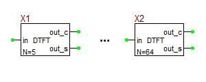
These blocks perform an N-point discrete-time Fourier transform (DTFT) of their input signal and output the transform as two temporal voltage signals representing the cosine and sine DTFT transforms. The The input signal of these block can be either a continuous-time signal or a pulse train of the specified period.
There are ten DTFT blocks for N = 5, 6, 7, 8, 9, 10, 12, 16, 32, 64. In each case, the total duration of the transform window is NT, where T is the sampling period.
Parameters:
| NAME | PARAMETER | UNITS | DEFAULT | NOTES |
|---|---|---|---|---|
| T | sampling period | sec | 1 | required |
| rise_time | window rise time | sec | 0 | |
| fall_time | window fall time | sec | 0 |
Discrete-Time Signal Hold Block
This device takes a pulse train of a specified period as its input and holds the value of each pulse's amplitude during each clock cycle at the output.
Parameters:
| NAME | PARAMETER | UNITS | DEFAULT | NOTES |
|---|---|---|---|---|
| T | sampling period | sec | 1 | required |
| duty_cycle | sampling pulse duty cycle | - | 0.1 | |
| rise_time | window rise time | sec | 0 | |
| fall_time | window fall time | sec | 0 | |
| Tmax | signal period or maximum duration | sec | 10 |
Divider Block
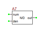
The Divider Block has two inputs. Each of the numerator and denominator inputs is added to its respective offset and then multiplied by its respective input gain (with default values of 1). Next, the loaded numerator signal is divided by the loaded denominator signal. The result is multiplied by the output gain and then added to the output offset. To avoid division by zero, the divider function sets the denominator signal greater than zero through the lower limit parameter. This limit is approached through a quadratic smoothing function, the domain of which may be specified as a fraction of the lower limit value or as an absolute value. The divider function operates in DC, AC, and Transient analysis modes. In AC analysis, however, it is important to remember that results are invalid unless the denominator input is a DC voltage.
Model Identifier: divide
Netlist Format:
A<device_name> <num_pin> <den_pin> <out_pin> <model_name>
.model <model_name> divide {<param1 = value> < param2 = value> ...}
Example:
A1 1 2 3 divider_block
.model divider_block divide den_offset = 0.0 den_gain = 1.0
Parameters:
| NAME | PARAMETER | UNITS | DEFAULT | NOTES |
|---|---|---|---|---|
| num_offset | numerator offset | V | 0.0 | |
| num_gain | numerator gain | - | 1.0 | |
| den_offset | denominator offset | V | 0.0 | |
| den_gain | denominator gain | - | 1.0 | |
| den_lower_limit | denominator lower limit | V | 1.0e-10 | |
| den_domain | denominator smoothing domain | - | 1.0e-10 | |
| fraction | smoothing fraction/absolute value switch | - | False | |
| out_gain | output gain | - | 1.0 | |
| out_offset | output offset | V | 0.0 |
Finite Sequence Pulse Generator
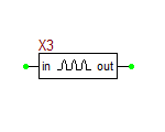
This is a voltage source that generates a pulse train of finite duration oscillating between zero and a user defined maximum voltage level.
Parameters:
| NAME | PARAMETER | UNIT | DEFAULT | NOTES |
|---|---|---|---|---|
| T | pulse period | sec | 1m | required |
| w | pulse width | sec | 0.5m | required |
| n | number of pulses | - | 5 | |
| rise_time | pulse rise time | sec | 0 | |
| fall_time | pulse fall time | sec | 0 | |
| max_val | maximum output voltage level | V | 1 | |
| start | start time | sec | 0 |
Finite Sequence Random Pulse Generator
This is a voltage source that generates a finite sequence of random pulses with a user defined number of random levels. By default, both the pulse amplitude and pulse width are randomized. You have the option to fix either of these parameters.
Parameters:
| NAME | PARAMETER | UNIT | DEFAULT | NOTES |
|---|---|---|---|---|
| period | period | sec | 1 | required |
| duty_cycle | pulse duty cycle | - | 0.5 | required |
| random_amp | 1 for random amplitude, 0 otherwise | - | 1 | |
| random_wid | 1 for random pulse width, 0 otherwise | - | 1 | |
| n_rand | number of random levels | - | 10 | |
| rise_time | pulse rise time | sec | 0 | |
| fall_time | pulse fall time | sec | 0 | |
| max_val | maximum output voltage level | V | 1 | |
| n_val | number of random pulses | - | 5 | |
| start | start time | sec | 0 |
Finite Sequence Signal Sampler Block
This device samples its input signal during a finite time window at a specified sampling period and outputs a pulse train of finite duration with a specified duty cycle.
Parameters:
| NAME | PARAMETER | UNITS | DEFAULT | NOTES |
|---|---|---|---|---|
| T | sampling period | sec | 1 | required |
| duty_cycle | sampling pulse duty cycle | - | 0.01 | |
| rise_time | window rise time | sec | 0 | |
| fall_time | window fall time | sec | 0 | |
| n | number of samples | - | 5 | |
| start | start time | sec | 0 |
Frequency Detector Block
This device measures the frequency of a harmonic input signal and produces a voltage proportional to the frequency in Hz at the output. It can also be used as a frequency converter.
Parameters:
| NAME | PARAMETER | UNITS | DEFAULT | NOTES |
|---|---|---|---|---|
| r_in | input resistance | Ω | 1G | |
| r_out | output resistance | Ω | 1u | |
| K_v | voltage conversion factor | V/Hz | 1e-6 | |
| max_in | input amplitude | V | 1 |
Frequency Doubler Block
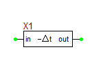
This device takes a harmonic input signal and generates a harmonic output signal with twice the frequency and a user specified amplitude.
Parameters:
| NAME | PARAMETER | UNITS | DEFAULT | NOTES |
|---|---|---|---|---|
| r_in | input resistance | Ω | 1G | |
| r_out | output resistance | Ω | 1u | |
| max_val | output amplitude | V | 1.0 |
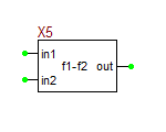
Frequency Down-Converter Block
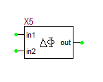
This 3-pin device takes two harmonic input signals with different frequencies fLO and fIF and generates a harmonic output signal with a frequency equal to fRF = fLO - fIF and a user specified amplitude.
Parameters:
| NAME | PARAMETER | UNITS | DEFAULT | NOTES |
|---|---|---|---|---|
| r_in | input resistance | Ω | 1G | |
| r_out | output resistance | Ω | 1u | |
| max_in | peak amplitude of both inputs | V | 1.0 | Both inputs must have equal amplitudes. |
| max_out | output amplitude | V | 1.0 |
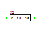
Frequency Modulator Block
This device takes an input signal and generates an FM modulated output signal of a specified carrier frequency with a specified maximum frequency deviation.
Parameters:
| NAME | PARAMETER | UNITS | DEFAULT | NOTES |
|---|---|---|---|---|
| r_in | input resistance | Ω | 1G | |
| r_out | output resistance | Ω | 1u | |
| f_del | maximum frequency deviation | Hz | 500k | |
| fc | carrier frequency | Hz | 1Meg | |
| ac | carrier peak amplitude | V | 1 |
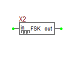
Frequency Shift-Keying Modulator Block
This device takes a digital input like a binary sequence and generates an FSK modulated output signal with two specified carrier frequencies.
Parameters:
| NAME | PARAMETER | UNITS | DEFAULT | NOTES |
|---|---|---|---|---|
| r_out | output resistance | Ω | 1u | |
| fc_lo | low carrier frequency | Hz | 1Meg | |
| fc_hi | high carrier frequency | Hz | 2Meg | |
| ac | carrier peak amplitude | V | 1.0 |
Frequency Up-Converter Block
This 3-pin device takes two harmonic input signals with different frequencies fLO and fIF and generates a harmonic output signal with a frequency equal to fRF = fLO + fIF and a user specified amplitude.
Parameters:
| NAME | PARAMETER | UNITS | DEFAULT | NOTES |
|---|---|---|---|---|
| r_in | input resistance | Ω | 1G | |
| r_out | output resistance | Ω | 1u | |
| max_in | peak amplitude of both inputs | V | 1.0 | both inputs must have equal amplitudes. |
| max_out | output amplitude | V | 1.0 |
Gain Block
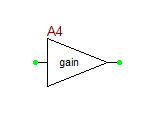
This model is a simple gain block with optional offsets on the input and the output. In_offset is added to the input, the sum of which is then multiplied by the gain, and the output offset is added to produce the final output. The gain block model will operate in DC, AC, and Transient analysis modes.
Model Identifier: gain
Netlist Format:
A<device_name> <in_pin> <out_pin> <model_name>
.model <model_name> gain {<param1 = value> < param2 = value> ...}
Example:
A1 1 2 gain_block
.model gain_block gain in_offset = 0.0 out_offset = 0.0
Parameters:
| NAME | PARAMETER | UNITS | DEFAULT | NOTES |
|---|---|---|---|---|
| in_offset | input offset | V | 0.0 | |
| gain | gain | - | 1.0 | |
| out_offset | out_offset | V | 0.0 |
Generalized Analog Filter Block
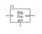
This block models a generalize analog filter characterized by a rational transfer functions in the spectral domain Laplace variable s:
[math] H(s) = \frac{N(s)}{D(s)} = \frac{ \sum_{m=0}^{M} b_m s^m }{ \sum_{n=0}^{N} a_n s^n } [/math]
subject to the requirement N ≥ M and aN = 1. To access the parameters of this block, you have to click the Edit Model... button of its property dialog.
The functionality of this block, which is native to RF.Spice A/D, is very similar to the s-domain transfer function block, which is an XPSICE process model. This block does not have a denormalization frequency parameter. Therefore, at frequencies other than the unit frequency, the transfer function must be explicitly scaled. This block can be used in conjunction with both transient and AC frequency sweep tests.
Parameters:
| NAME | PARAMETER | UNITS | DEFAULT | NOTES |
|---|---|---|---|---|
| deg | highest degree of s in transfer function | - | 2 | required |
| coeff_den | denominator coefficients array: coefficients of powers of s, highest power first | - | 1 0 1 | required |
| coeff_num | numerator coefficients array: coefficients of powers of s, highest power first | - | 0 0 1 | required |
| r_in | input resistance | Ω | 10G | |
| r_out | output resistance | Ω | 1u |
Generalized Digital Filter Block
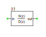
This block models a generalized digital filter characterized by a rational transfer functions in the Z-transform domain variable z:
[math] H(z) = \frac{N(z)}{D(z)} = \frac{ \sum_{m=0}^{M} b_m z^m }{ \sum_{n=0}^{N} a_n z^n } [/math]
subject to the requirement N ≥ M. To access the parameters of this block, you have to click the Edit Model... button of its property dialog.
Parameters:
| NAME | PARAMETER | UNITS | DEFAULT | NOTES |
|---|---|---|---|---|
| deg | highest degree of z in transfer function | - | 2 | required |
| coeff_den | denominator coefficients array: coefficients of powers of (-z1/2), highest power first | - | 1 0 1 0 1 | required |
| coeff_num | numerator coefficients array: coefficients of powers of (-z1/2), highest power first | - | 1 0 0 0 0 | required |
| freq | sampling frequency | Hz | 1 | required |
Generic Bandpass Filter Block
This device is a generic bandpass filter with user specified center frequency and bandwidth. It is based on a fifth-order Butterworth LC ladder topology.
Parameters:
| NAME | PARAMETER | UNITS | DEFAULT | NOTES |
|---|---|---|---|---|
| f0 | center frequency | Hz | 1Meg | |
| bw | bandwidth | Hz | 200k | |
| r0 | source/load resistance | Ω | 50 |
Generic Bandstop Filter Block
This device is a generic bandstop filter with user specified center frequency and bandwidth. It is based on a fifth-order Butterworth LC ladder topology.
Parameters:
| NAME | PARAMETER | UNITS | DEFAULT | NOTES |
|---|---|---|---|---|
| f0 | center frequency | Hz | 1Meg | |
| bw | bandwidth | Hz | 200k | |
| r0 | source/load resistance | Ω | 50 |
Generic Highpass Filter Block
This device is a generic highpass filter with a user specified cutoff frequency. It is based on a fifth-order Butterworth LC ladder topology.
Parameters:
| NAME | PARAMETER | UNITS | DEFAULT | NOTES |
|---|---|---|---|---|
| cutoff | cutoff frequency | Hz | 1Meg | |
| r0 | source/load resistance | Ω | 50 |
Generic Lowpass Filter Block
This device is a generic lowpass filter with a user specified cutoff frequency. It is based on a fifth-order Butterworth LC ladder topology.
| NAME | PARAMETER | UNITS | DEFAULT | NOTES |
|---|---|---|---|---|
| cutoff | cutoff frequency | Hz | 1Meg | |
| r0 | source/load resistance | Ω | 50 |
Geometric Mean Block
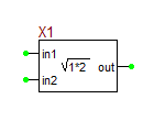
This 3-pin device sends the geometric mean of its two inputs to the output with a default unity gain.
Parameters:
| NAME | PARAMETER | UNITS | DEFAULT | NOTES |
|---|---|---|---|---|
| gain | gain | - | 1.0 |
Gudermannian Polarity Detector Block
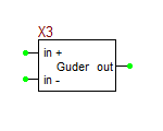
This 3-pin device measures the difference signal Δv = vpos - vneg and produces an output proportional to the Gudermannian function of Δv:
[math] v_{out} = A \cdot \frac{2}{\pi} \ gd(a\Delta v) = A \cdot \left( \frac{4}{\pi} \tan^{-1}(e^{a\Delta v}) - 1 \right) [/math]
Parameters:
| NAME | PARAMETER | UNITS | DEFAULT | NOTES |
|---|---|---|---|---|
| a | shaping Constant | - | 10 | |
| MaxVal | output amplitude | V | 1 |
Ideal Buffer Block
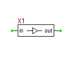
This model is an ideal buffer block with a default unity gain.
Parameters:
| NAME | PARAMETER | UNITS | DEFAULT | NOTES |
|---|---|---|---|---|
| r_in | input resistance | Ω | 1G | |
| r_out | output resistance | Ω | 1u | |
| gain | gain | - | 1.0 |
Ideal Comparator Block
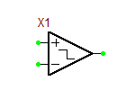
This block is an ideal two-signal voltage comparator with a default unity gain. It has a binary output that takes a value of 0V if vpos < vneg and takes a value of 1V if vpos > vneg. If vpos = vneg, the output voltage is 0.5V.
Parameters:
| NAME | PARAMETER | UNITS | DEFAULT | NOTES |
|---|---|---|---|---|
| gain | comparator gain | - | 1.0 |
Ideal Delay Block
This model is an ideal signal delay block based on an ideal delay line model.
Parameters:
| NAME | PARAMETER | UNITS | DEFAULT | NOTES |
|---|---|---|---|---|
| delay | time delay | sec | 1u |
Ideal Full-Wave Rectifier Block
This block rectifies an input signal at both positive and negative cycles with a default unity gain.
Parameters:
| NAME | PARAMETER | UNITS | DEFAULT | NOTES |
|---|---|---|---|---|
| gain | rectifier gain | - | 1.0 |
Ideal Gyrator Block
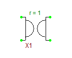
An ideal gyrator is a linear two-port device which couples the current on one port to the voltage on the other and vice versa. The instantaneous voltages and currents instantaneous are related by:
- [math]v_{out}(t) = R \cdot i_{in}(t) [/math]
- [math]v_{in}(t) = - R \cdot i_{out}(t) [/math]
The ideal gyrator acts as an impedance inverter.
Parameters:
| NAME | PARAMETER | UNITS | DEFAULT | NOTES |
|---|---|---|---|---|
| r | gyration resistance | Ω | 1.0 |
Ideal Half-Wave Rectifier Block
This block rectifies an input signal at positive cycles with a default unity gain. Its output at negative cycles is zero.
Parameters:
| NAME | PARAMETER | UNITS | DEFAULT | NOTES |
|---|---|---|---|---|
| gain | rectifier gain | - | 1.0 |
Ideal Phase Shifter Block
This model is an ideal signal phase shifter block based on an ideal transmission line segment model. It is frequency-dependent and the signal phase shift is accurate only around the specified center frequency.
Parameters:
| NAME | PARAMETER | UNITS | DEFAULT | NOTES |
|---|---|---|---|---|
| phi | phase shift | deg | 90 | must be positive |
| fo | center frequency | Hz | 1Meg |
Ideal Polarity Detector Block
This 3-pin device measures the difference signal Δv = vpos - vneg and produces a binary output ±A according to the sign of Δv, where A is a user defined amplitude.
Parameters:
| NAME | PARAMETER | UNITS | DEFAULT | NOTES |
|---|---|---|---|---|
| MaxVal | output amplitude | V | 1 |
Ideal Splitter Block
This model is an ideal signal splitter block with a default one-half split ratio. It splits the input signal by a ratio of k:(1-k).
Parameters:
| NAME | PARAMETER | UNITS | DEFAULT | NOTES |
|---|---|---|---|---|
| k | split ratio | - | 0.5 |
Impulse Generator
This is a voltage source that generates a periodic impulse train with oscillating between zero and a user defined maximum voltage level.
Parameters:
| NAME | PARAMETER | UNIT | DEFAULT | NOTES |
|---|---|---|---|---|
| T | impulse period | sec | 1u | required |
| duty_cycle | impulse duty cycle | - | 0.01 | required |
| max_val | maximum output voltage level | V | 1 | |
| delay | delay time | sec | 0 |
Integer Modulo Block
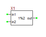
This 3-pin device requires a voltage with an integer value on its second input pin. It produces a voltage equal to vin1 % vin2 and sends it to the output with a default unity gain.
Parameters:
| NAME | PARAMETER | UNITS | DEFAULT | NOTES |
|---|---|---|---|---|
| gain | gain | - | 1.0 |
Integrator Block
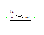
The Integrator Gain and input offset parameters are also included to allow for tailoring of the required signa. Output upper and lower limits are also included to prevent convergence errors resulting from excessively large output values. Note that these limits specify integrator behavior similar to that found in an operational amplifier-based integration stage, in that once a limit is reached, additional storage does not occur. Thus the input of a negative value to an integrator which is currently driving at the out_upper_limit level will immediately cause a drop in the output, regardless of how long the integrator was previously summing positive inputs. The incremental value of output below the output_upper_limit and above the output_lower_limit at which smoothing begins is specified via the limit_range parameter. In AC analysis, the value returned is equal to the gain divided by the radian frequency of analysis.
Note that truncation error checking is included in the \93int\94 block. This should provide for a more accurate simulation for the time integration function, since the model will inherently request smaller time increments between simulation points if truncation errors would otherwise be excessive.
Model Identifier: int
Netlist Format:
A<device_name> <in_pin> <out_pin> <model_name>
.model <model_name> int out_lower_limit = <value> out_upper_limit = <value> {<param1 = value> < param2 = value> ...}
Example:
A1 1 2 integrator_block
.model integrator_block int out_lower_limit = -1t out_upper_limit = 1t
Parameters:
| NAME | PARAMETER | UNITS | DEFAULT | NOTES |
|---|---|---|---|---|
| gain | gain | - | 1.0 | |
| in_offset | output offset | V | 0.0 | |
| out_lower_limit | output lower limit | V | -1t | required |
| out_upper_limit | output upper limit | V | 1t | required |
| limit_range | upper and lower limit smoothing range | - | 1.0e-6 | |
| out_ic | output initial condition | V | 0.0 |
Leading Edge Detector Block
This device follows its input signal and produces an output at the specified low voltage level. Every time a leading edge of the input signal is detected, that is vin crosses the specified threshold level from a lower value to a high value, a short pulse of the specified width with an amplitude equal to the specified high voltage level is generated at the output.
Parameters:
| NAME | PARAMETER | UNITS | DEFAULT | NOTES |
|---|---|---|---|---|
| Vt | threshold voltage | V | 0.5 | |
| out_low | low output voltage level | V | 0 | |
| out_high | high output voltage level | v | 1 | |
| pulse_wid | output pulse width | sec | 0.1u |
Limiter Block
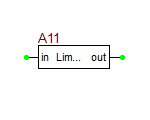
The Limiter is a single-input, single-output block similar to the Gain Block. However, the output of the Limiter function is restricted to the range specified by the output lower and upper limits. This model operates in DC, AC and Transient analysis modes. Note that the limit range is the value below the UPPER LIMIT and above the LOWER LIMIT at which smoothing of the output signal begins. For this model, then, the limit range represents the delta with respect to the output level at which smoothing occurs. Thus, for an input gain of 2.0 and output limits of 1.0 and -1.0 volts, the output will begin to smooth out at �+/-0.9 volts, which occurs when the input value is at 0.4V.
Model Identifier: limit
Netlist Format:
A<device_name> <in_pin> <out_pin> <model_name>
.model <model_name> limit {<param1 = value> < param2 = value> ...}
Example:
A1 1 2 limit_block
.model limit_block limit in_offset = 0.0 gain = 1.0 out_lower_limit = -1t out_upper_limit = 1t
Parameters:
| NAME | PARAMETER | UNITS | DEFAULT | NOTES |
|---|---|---|---|---|
| in_offset | input offset | V | 0.0 | |
| gain | gain | - | 1.0 | |
| out_lower_limit | output lower limit | V | 0.0 | |
| out_upper_limit | output upper limit | V | 1.0 | |
| limit_range | upper and lower smoothing range | - | 1.0e-6 | |
| fraction | smoothing fraction/absolute value switch | - | False |
Link Propagation Block
This block models a receiver signal in a free-space, line-of-sight (LOS) communication link. It takes the input signal and attenuates and delays it at the output based on Friis' equation for the specified range.
Parameters:
| NAME | PARAMETER | UNITS | DEFAULT | NOTES |
|---|---|---|---|---|
| range | distance between transmitter and receiver | m | 1.0 | |
| fo | frequency | Hz | 1Meg | |
| G_Tx | transmit antenna gain in dB | - | 0 | |
| G_Rx | receive antenna gain in dB | - | 0 |
Maximum Detector Block
This device follows its input voltage and holds its maximum value at the output.
Parameters:
| NAME | PARAMETER | UNITS | DEFAULT | NOTES |
|---|---|---|---|---|
| r_in | input resistance | Ω | 1G | |
| r_out | output resistance | Ω | 1u |
Maximum Selector Block
This 3-pin device selects the larger of its two inputs and sends it to the output with a default unity gain.
Parameters:
| NAME | PARAMETER | UNITS | DEFAULT | NOTES |
|---|---|---|---|---|
| gain | gain | - | 1.0 |
Minimum Detector Block
This device follows its input voltage and holds its minimum value at the output.
Parameters:
| NAME | PARAMETER | UNITS | DEFAULT | NOTES |
|---|---|---|---|---|
| r_in | input resistance | Ω | 1G | |
| r_out | output resistance | Ω | 1u |
Minimum Selector Block
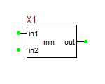
This 3-pin device selects the smaller of its two inputs and sends it to the output with a default unity gain.
Parameters:
| NAME | PARAMETER | UNITS | DEFAULT | NOTES |
|---|---|---|---|---|
| gain | gain | - | 1.0 |
Multiplier Block
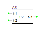
The Multiplier Block has two inputs. Each input is added to its respective offset and then multiplied by the specified input gain (with default values of 1). These are then multiplied along with the output gain and the result is added to the output offset. Note that the input offsets and input gains are specified as vectors. The multiplier function operates in DC, AC, and Transient analysis modes. In AC analysis, however, it is important to remember that results are invalid unless one of the inputs is a DC voltage.
Model Identifier: mult
Netlist Format:
A<device_name> [<in_pin1> <in_pin2> {...}] <out_pin> <model_name>
.model <model_name> mult {<param1 = value> < param2 = value> ...}
Example:
A1 [1 2] 3 mult_block
.model mult_block mult in_offset = [0.0 0.0] in_gain = [1.0 1.0] out_gain = 1.0 out_offset = 0.0
Parameters:
| NAME | PARAMETER | UNITS | DEFAULT | NOTES |
|---|---|---|---|---|
| in_offset | input offset vector | V | [0.0 0.0] | |
| in_gain | input gain vector | - | [1.0 1.0] | |
| out_gain | output gain | - | 1.0 | |
| out_offset | output offset | V | 0.0 |
One-Shot Sample-and-Hold Block
This device follows its input signal and samples it at a specified instant of time. It holds the value of that sample at its output indefinitely.
Parameters:
| NAME | PARAMETER | UNITS | DEFAULT | NOTES |
|---|---|---|---|---|
| T | sampling period | sec | 1 | required |
| Tmax | signal period or maximum duration | sec | 10 |
Peak Detector Block
This device follows its input voltage and holds its peak value (the greater of the absolute values of its maximum or minimum) at the output.
Parameters:
| NAME | PARAMETER | UNITS | DEFAULT | NOTES |
|---|---|---|---|---|
| r_in | input resistance | Ω | 1G | |
| r_out | output resistance | Ω | 1u |
Phase Detector Block
This 3-pin device measures the phase difference between two harmonic input signals of the same frequency and produces a voltage proportional to the phase difference in radians at the output. Only the absolute phase difference is detected. This block cannot determine phase lead or phase lag.
Parameters:
| NAME | PARAMETER | UNITS | DEFAULT | NOTES |
|---|---|---|---|---|
| r_in | input resistance | Ω | 1G | |
| r_out | output resistance | Ω | 1u | |
| K_v | voltage conversion factor | V/rad | 1 |
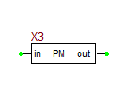
Phase Modulator Block
This device takes an input signal and generates an PM modulated output signal of a specified carrier frequency with a specified maximum phase deviation.
Parameters:
| NAME | PARAMETER | UNITS | DEFAULT | NOTES |
|---|---|---|---|---|
| r_in | input resistance | Ω | 1G | |
| r_out | output resistance | Ω | 1u | |
| phi_del | maximum phase deviation | rad | π | |
| fc | carrier frequency | Hz | 1Meg | |
| ac | carrier peak amplitude | V | 1 | |
| phi0 | carrier phase | rad | 0 |
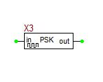
Phase Shift-Keying Modulator Block
This device takes a digital input like a binary sequence and generates a PSK modulated output signal with two specified carrier phase values.
Parameters:
| NAME | PARAMETER | UNITS | DEFAULT | NOTES |
|---|---|---|---|---|
| r_out | output resistance | Ω | 1u | |
| phi_lo | low carrier phase value | rad | 0 | |
| phi_hi | high carrier phase value | rad | π | |
| fc | carrier frequency | Hz | 1Meg | |
| ac | carrier peak amplitude | V | 1.0 |
Piecewise Linear Map Block
This 3-pin device provides a linear mapping of the input signal onto the output signal. The piecewise linear map is define in the XY plane by a start point, an end point, and N breakpoints between them.
Parameters:
| NAME | PARAMETER | UNITS | DEFAULT | NOTES |
|---|---|---|---|---|
| startX | starting value of X | V | 0 | required |
| startY | starting value of Y | V | 0 | required |
| breakpointN | number of breakpoints | - | 2 | required |
| breakpointX | breakpoints for X | V | 1 2 | required |
| breakpointY | breakpoints for Y | V | 1 4 | required |
| finalX | final value of X | V | 3 | required |
| finalY | final value of Y | V | 9 | required |
| r_in | input resistance | Ω | 10G | |
| r_out | output resistance | Ω | 1u |
Polar-to-Rect Coordinates Conversion Block
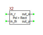
This 4-pin device takes two input signals as the radius and angle coordinates (ρ, φ) on a plane and generates the equivalent Cartesian coordinates as two output voltage signals: X and Y, with optional gains. The angle input signal must be expressed in radians.
Parameters:
| NAME | PARAMETER | UNITS | DEFAULT | NOTES |
|---|---|---|---|---|
| out_gain1 | output gain | - | 1.0 |
Pulse Generator
This is a voltage source that generates a periodic pulse train with user defined low and high voltage levels.
Parameters:
| NAME | PARAMETER | UNIT | DEFAULT | NOTES |
|---|---|---|---|---|
| fo | frequency | Hz | 1Meg | required |
| duty_cycle | pulse duty cycle | - | 0.5 | required |
| delay | delay time | sec | 0 | |
| rise_time | pulse rise time | sec | 0 | |
| fall_time | pulse fall time | sec | 0 | |
| out_low | low output voltage level | V | -1 | |
| out_high | high output voltage level | V | +1 |
Pulse Width Modulator Block
This device takes an input signal and compares it to an internally generated ramp signal with a specified period and generates a binary PWM modulated output signal. A designated pin provides the ramp signal output.
Parameters:
| NAME | PARAMETER | UNITS | DEFAULT | NOTES |
|---|---|---|---|---|
| r_in | input resistance | Ω | 1G | |
| r_out | output resistance | Ω | 1u | |
| V_lo | low output voltage level | V | 0 | |
| V_hi | high output voltage level | V | 1 | |
| V_lo | hysteresis voltage tolerance | V | 100m | |
| T_rmp | sampling period | sec | 1m | |
| rmp_lo | ramp minimum voltage level | V | 0 | |
| rmp_hi | ramp maximum voltage level | V | 1 | |
| duty_cycle | ramp duty cycle | - | 0.01 | Must be between 0.01 and 0.99 |
Quadrature Amplitude Modulator Block
This 3-pin device takes two input signals and generates a QAM modulated output signal of a specified carrier frequency:
[math] v_{out}(t) = A_c \left( v_{in_I}(t) \cdot \cos(2\pi f_c t) + v_{in_Q}(t) \cdot \sin(2\pi f_c t) \right) [/math]
Parameters:
| NAME | PARAMETER | UNITS | DEFAULT | NOTES |
|---|---|---|---|---|
| r_in | input resistance | Ω | 1G | |
| r_out | output resistance | Ω | 1u | |
| fc | carrier frequency | Hz | 1Meg | |
| ac | carrier peak amplitude | V | 1 |
Quadrature Harmonic Wave Generator
This is a 3-pin voltage source that generates two sinusoidal wave outputs with a 90° phase difference.
Parameters:
| NAME | PARAMETER | UNIT | DEFAULT | NOTES |
|---|---|---|---|---|
| fo | frequency | Hz | 1Meg | required |
| max_val | maximum output voltage level | V | 1 | |
| Vo | offset DC voltage | V | 0 | |
| Td | delay time | sec | 0 |
Radar Echo Block
This block models a radar echo signal. It takes the input signal and attenuates and delays it at the output based on the radar equation given the target range and its specified RCS.
Parameters:
| NAME | PARAMETER | UNITS | DEFAULT | NOTES |
|---|---|---|---|---|
| range | target range | m | 1.0 | |
| fo | frequency | Hz | 1Meg | |
| sigma | target RCS | m2 | 1.0 | |
| G_Tx | transmit antenna gain in dB | - | 0 | |
| G_Rx | receive antenna gain in dB | - | 0 |
Ramp Generator
This is a voltage source that generates a periodic ramp also known as a sawtooth waveform with user defined low and high voltage levels. You can define either an up-ramp or a down-ramp.
Parameters:
| NAME | PARAMETER | UNIT | DEFAULT | NOTES |
|---|---|---|---|---|
| T | ramp period | sec | 1m | required |
| out_low | low output voltage level | V | -1 | |
| out_high | high output voltage level | V | +1 | |
| ramp_type | 0 for up-ramp, 1 for down-ramp | - | 0 |
Random Digitized Signal Generator
This is a voltage source that generates a periodic random digitized signal with a user defined number of random levels.
Parameters:
| NAME | PARAMETER | UNIT | DEFAULT | NOTES |
|---|---|---|---|---|
| period | sampling period | sec | 1 | required |
| n_rand | number of random levels | - | 10 | |
| max_val | maximum output voltage level | V | 1 |
Random Noise Generator
This is a periodic noise generator with user defined peak-to-peak amplitude fluctuation.
Parameters:
| NAME | PARAMETER | UNIT | DEFAULT | NOTES |
|---|---|---|---|---|
| vpp | peak-to-peak amplitude | V | 0.1 | required |
| offset | offset voltage | V | 0 | |
| period | period | sec | 1m | required |
Random Pulse Generator
This is a voltage source that generates a periodic random pulse train with a user defined number of random levels. By default, both the pulse amplitude and pulse width are randomized. You have the option to fix either of these parameters.
Parameters:
| NAME | PARAMETER | UNIT | DEFAULT | NOTES |
|---|---|---|---|---|
| period | period | sec | 1 | required |
| duty_cycle | pulse duty cycle | - | 0.5 | required |
| random_amp | 1 for random amplitude, 0 otherwise | - | 1 | |
| random_wid | 1 for random pulse width, 0 otherwise | - | 1 | |
| n_rand | number of random levels | - | 10 | |
| rise_time | pulse rise time | sec | 0 | |
| fall_time | pulse fall time | sec | 0 | |
| max_val | maximum output voltage level | V | 1 |
Range-Crossing Detector Block
This 4-pin device compares its input signal to two different reference voltages. If detects the events every time vin becomes less than vref1 or greater than vref2. If vref1 ≤ vin ≤ vref2, the output is zero. If vin < vref1, the output switches to -A, and if vin > vref2, the output switches to +A.
Parameters:
| NAME | PARAMETER | UNITS | DEFAULT | NOTES |
|---|---|---|---|---|
| max_val | output amplitude | V | 1 |
Rect-to-Polar Coordinates Conversion Block
This 4-pin device takes two input signals as the X and Y coordinates on a plane and generates the equivalent polar coordinates as two output voltage signals: radius and angle, with optional gains. The angle output signal is expressed in radians.
Parameters:
| NAME | PARAMETER | UNITS | DEFAULT | NOTES |
|---|---|---|---|---|
| out_gain1 | gain of radius output | - | 1.0 | |
| out_gain2 | gain of angle output | - | 1.0 |
S-Domain Transfer Function Block
The s-domain transfer function is a single input and output transfer function in the Laplace transform variable \93s\94 that allows for flexible modulation of the frequency-domain characteristics of a signal. The code model may be configured to produce an arbitrary s-domain transfer function with the following restrictions:
1. The degree of the numerator polynomial cannot exceed that of the denominator polynomial in the variable \93s\94.
2. The coefficients for a polynomial must be stated explicitly. That is, if a coefficient is zero, it must be included as an input to the num_coeff or den_coeff vector.
Gain and input offset parameters are included to allow for tailoring of the required signal. Internal signal values and the output value of the s-domain transfer function do not have limits, so you are cautioned to specify gain and coefficient values that will not cause the model to produce excessively large values. In AC analysis, the value returned is equal to the real and imaginary components of the total s-domain transfer function at each frequency of interest.
The denormalized_freq term allows you to specify coefficients for a normalized filter (i.e., one in which the frequency of interest is 1 rad/s) Once these coefficients are included, specifying the denormalized frequency value \93shifts\94 the corner frequency to the actual one of interest.
Truncation error checking is included in the s-domain transfer block. This should provide for more accurate simulations, since the model will inherently request smaller time increments between simulations points if truncation errors would otherwise be excessive.
The order of the coefficient parameters is from that associated with the highest-powered term decreasing to that of the lowest.
Model Identifier: s_xfer
Netlist Format:
A<device_name> <in_pin> <out_pin> <model_name>
.model <model_name> s_xfer num_coeff = [<value1> {<value2>}...] den_coeff = [<value1> {<value2>}...]
+
int_ic = [<value1> {<value2>}...] {<param1 = value> < param2 = value> ...}
Example:
A 1 2 A_transfer_function
.model A_transfer_function s_xfer num_coeff = [1] den_coeff = [1] int_ic = [0.0]
Parameters:
| NAME | PARAMETER | UNITS | DEFAULT | NOTES |
|---|---|---|---|---|
| In_offset | input offset | V | 0.0 | |
| Gain | gain | - | 1.0 | |
| Num_coeff | numerator polynomial coefficients | - | [1] | required |
| Den_coeff | denominator polynomial coefficients | - | [1] | required |
| Int_ic | integrator stage initial conditions | V | [0.0] | required |
| Denormalized_freq | denormalized corner frequency | rad/s | 1.0 |
Schmitt Trigger Block
This device is a 2-pin Schmitt trigger switch with hysteresis effect. In general, if vin < X1, then vout = Y1, and if vin > X2, then vout = Y2. If the output voltage is at its low level Y1 and you increase the input signal, the output switches to the high level Y2 as soon as vin > X2. If the output voltage is at its high level Y2 and you decrease the input signal, the output switches to the low level Y1 as soon as vin < X1. The flag INV converts the block into an inverting Schmitt trigger.
Parameters:
| NAME | PARAMETER | UNITS | DEFAULT | NOTES |
|---|---|---|---|---|
| r_in | input resistance | Ω | 1G | |
| r_out | output resistance | Ω | 1u | |
| X1 | lower input switching voltage level | V | -1.0 | |
| X2 | higher input switching voltage level | v | 1.0 | |
| Y1 | lower output voltage level | V | -1.0 | |
| Y2 | higher output voltage level | V | 1.0 | |
| INV | flag for inverting Schmitt trigger | - | False |
Sigmoid Polarity Detector Block
This 3-pin device measures the difference signal Δv = vpos - vneg and produces an output proportional to the Sigmoid function of Δv:
[math] v_{out} = A \cdot \left( 2S(a\Delta v) - 1 \right) = A \cdot \left( \frac{2}{1+\exp(-a\Delta v)} - 1 \right) [/math]
Parameters:
| NAME | PARAMETER | UNITS | DEFAULT | NOTES |
|---|---|---|---|---|
| a | shaping Constant | - | 10 | |
| MaxVal | output amplitude | V | 1 |
Signal Normalizer Block
This block normalizes an input signal by dividing its voltage by its maximum value.
Parameters:
None
Signal Sampler Block
This device samples its input signal at a specified sampling period and outputs a pulse train with a specified duty cycle.
Parameters:
| NAME | PARAMETER | UNITS | DEFAULT | NOTES |
|---|---|---|---|---|
| T | sampling period | sec | 1 | required |
| duty_cycle | sampling pulse duty cycle | - | 0.01 | |
| rise_time | window rise time | sec | 0 | |
| fall_time | window fall time | sec | 0 |
Sine-to-Square Wave Converter Block
This device converts an input sinusoidal signal to a square wave or pulse train of the same frequency and amplitude with an optional gain.
Parameters:
| NAME | PARAMETER | UNITS | DEFAULT | NOTES |
|---|---|---|---|---|
| gain | converter gain | - | 1 |
Sine Wave Chirp Generator
This is a voltage source that generates a sine wave output with sawtooth chirp modulation.
Parameters:
| NAME | PARAMETER | UNIT | DEFAULT | NOTES |
|---|---|---|---|---|
| period | chirp period | sec | 1u | required |
| freq_low | lower frequency value | Hz | 10Meg | required |
| freq_high | higher frequency value | Hz | 20Meg | required |
| max_val | maximum output voltage level | V | 1 | |
| chirp_type | 0 for up-chirp, 1 for down-chirp | - | 0 |
Sine Wave VCO Block
This device is a voltage-controlled oscillator block with a sinusoidal output signal.
Parameters:
| NAME | PARAMETER | UNITS | DEFAULT | NOTES |
|---|---|---|---|---|
| fo | free-running frequency | Hz | 1Meg | |
| K_f | frequency conversion factor | Hz/V | 500k | |
| max_val | output peak amplitude | V | 1 |
Slew Rate Block
This function limits the absolute slope of the output with respect to time to some maximum or value. The actual slew rate effects of over-driving an amplifier circuit can thus be accurately modeled by cascading the amplifier with this model. Maximum rising and falling slope values are in volts or amperes per second. Thus a desired slew rate of 0.5 V/us will be expressed as 0.5e+6, etc.
The slew rate block will continue to raise or lower its output until the difference between the input and the output values is zero. Thereafter, it will resume following the input signal, unless the slope again exceeds its rise or all slope limits. Whenever the model is slewing and the output comes to within the input +/- the range value, the partial derivative of the output with respect to the input will begin to smoothly transition from 0.0 to 1.0. Dout/din will equal 1.0 when the model is no longer slewing (output = input).
Model Identifier: slew
Netlist Format:
A<device_name> <in_pin> <out_pin> <model_name></P>
.model <model_name> slew {<param1 = value> < param2 = value> ...}
Example:
A1 1 2 slew_block
.model slew_block slew rise_slope = 1n fall_slope = 1n
Parameters:
| NAME | PARAMETER | UNITS | DEFAULT | NOTES |
|---|---|---|---|---|
| Rise_slope | maximum rising slope value | V/s | 1.0e9 | |
| Fall_slope | maximum falling slope value | V/s | 1.0e9 |
Slope Detector Block
This device follows its input signal and send its measured slope to the output with a default unity gain.
Parameters:
| NAME | PARAMETER | UNITS | DEFAULT | NOTES |
|---|---|---|---|---|
| r_in | input resistance | Ω | 1G | |
| r_out | output resistance | Ω | 1u | |
| gain | gain | - | 1.0 |
Square Wave Chirp Generator
This is a voltage source that generates a pulse train or square wave output with sawtooth chirp modulation.
Parameters:
| NAME | PARAMETER | UNIT | DEFAULT | NOTES |
|---|---|---|---|---|
| period | chirp period | sec | 1u | required |
| freq_low | lower frequency value | Hz | 10Meg | required |
| freq_high | higher frequency value | Hz | 20Meg | required |
| out_low | output lower limit | V | -1 | |
| out_high | output higher limit | V | +1 | |
| chirp_type | 0 for up-chirp, 1 for down-chirp | - | 0 |
Square Wave VCO Block
This device is a voltage-controlled oscillator block with a square wave output signal oscillating between two binary voltage levels.
Parameters:
| NAME | PARAMETER | UNITS | DEFAULT | NOTES |
|---|---|---|---|---|
| fo | free-running frequency | Hz | 1Meg | |
| K_f | frequency conversion factor | Hz/V | 500k | |
| duty_cycle | pulse duty cycle | - | 0.5 | |
| rise_time | pulse rise time | sec | 1n | |
| fall_time | pulse fall time | sec | 1n | |
| out_low | output lower limit | V | -1.0 | |
| out_high | output higher limit | V | -1.0 |
Summer Block
The Summer Block has two inputs. Each input is added to its respective offset and then multiplied by the specified input gain (with default values of 1). These are then summed, multiplied by the output gain and added to the output offset. Note that the input offsets and input gains are specified as vectors. The summer function operates in DC, AC, and Transient analysis modes.
Model Identifier: summer
Netlist Format:
A<device_name> <in_pin> <out_pin> <model_name>
.model <model_name> summer {<param1 = value> < param2 = value> ...}
Example:
A1 [1 2] 3 summer
.model summer summer in_offset = [0 0] in_gain = [1 1] out_gain = 1.0 out_offset = 0.0
Parameters:
| NAME | PARAMETER | UNITS | DEFAULT | NOTES |
|---|---|---|---|---|
| in_offset | input offset vector | V | [0 0] | |
| in_gain | input gain vector | - | [1 1] | |
| out_gain | output gain | - | 1.0 | |
| out_offset | output offset | V | 0.0 |
Temporal Window Block
This device gates its input signals in time from instant t = T1 to instant t = T2.
Parameters:
| NAME | PARAMETER | UNITS | DEFAULT | NOTES |
|---|---|---|---|---|
| T1 | start time | sec | 0 | |
| T2 | stop time | sec | 1m | |
| rise_time | window rise time | sec | 0 | |
| fall_time | window fall time | sec | 0 |
Trailing Edge Detector Block
This device follows its input signal and produces an output at the specified low voltage level. Every time a trailing edge of the input signal is detected, that is vin crosses the specified threshold level from a higher value to a lower value, a short pulse of the specified width with an amplitude equal to the specified high voltage level is generated at the output.
Parameters:
| NAME | PARAMETER | UNITS | DEFAULT | NOTES |
|---|---|---|---|---|
| Vt | threshold voltage | V | 0.5 | |
| out_low | low output voltage level | V | 0 | |
| out_high | high output voltage level | v | 1 | |
| pulse_wid | output pulse width | sec | 0.1u |
Triangular-to-Sine Wave Converter Block
This device converts an input triangular wave signal to a sinusoidal signal of the same frequency and amplitude with an optional gain.
Parameters:
| NAME | PARAMETER | UNITS | DEFAULT | NOTES |
|---|---|---|---|---|
| gain | converter gain | - | 1 |
Triangular-to-Square Wave Converter Block
This device converts an input triangular wave signal to a square wave or pulse train of the same frequency with a specified peak amplitude.
Parameters:
| NAME | PARAMETER | UNITS | DEFAULT | NOTES |
|---|---|---|---|---|
| max_val | output peak amplitude | V | 1 |
Triangular Wave Chirp Generator
This is a voltage source that generates a triangular wave output with sawtooth chirp modulation.
Parameters:
| NAME | PARAMETER | UNIT | DEFAULT | NOTES |
|---|---|---|---|---|
| period | chirp period | sec | 1u | required |
| freq_low | lower frequency value | Hz | 10Meg | required |
| freq_high | higher frequency value | Hz | 20Meg | required |
| out_low | output lower limit | V | -1 | |
| out_high | output higher limit | V | +1 | |
| chirp_type | 0 for up-chirp, 1 for down-chirp | - | 0 |
Triangular Wave Generator
This is a voltage source that generates a triangular wave output oscillating between -A and A, where A is a user defined maximum voltage levels.
Parameters:
| NAME | PARAMETER | UNIT | DEFAULT | NOTES |
|---|---|---|---|---|
| fo | frequency | Hz | 1Meg | required |
| duty_cycle | pulse duty cycle | - | 0.5 | required |
| max_val | maximum output voltage level | V | 1 |
Triangular Wave VCO Block
This device is a voltage-controlled oscillator block with a triangular wave output signal oscillating between two binary voltage levels. The parameter "duty_cycle" has a default value of 0.5, generating a symmetric triangular output. In the limiting cases of duty_cycle = 0.99 and duty_cycle = 0.01, the output will have an up-ramp or a down-ramp sawtooth waveform, respectively.
Parameters:
| NAME | PARAMETER | UNITS | DEFAULT | NOTES |
|---|---|---|---|---|
| fo | free-running frequency | Hz | 1Meg | |
| K_f | frequency conversion factor | Hz/V | 500k | |
| duty_cycle | triangular waveform duty cycle | - | 0.5 | Must be between 0.01 and 0.99. |
| out_low | output lower limit | V | -1.0 | |
| out_high | output higher limit | V | -1.0 |
xN Frequency Multiplier Block
These devices take a harmonic input signal and generate a harmonic output signal with a frequency N times larger and a user specified amplitude: N = 3, 4, 5, 6, 7, 8, 9, 10.
Parameters:
| NAME | PARAMETER | UNITS | DEFAULT | NOTES |
|---|---|---|---|---|
| r_in | input resistance | Ω | 1G | |
| r_out | output resistance | Ω | 1u | |
| max_val | output amplitude | V | 1.0 |
Zero-Crossing Detector Block
This 3-pin device follows its input signal, detects its sign changes, and produces two binary outputs based on the zero crossings: Output 1 is a pulse train and Output 2 is an impulse train. Both output signals oscillate between -A and +A every time the input signal has a sign change.
Parameters:
| NAME | PARAMETER | UNITS | DEFAULT | NOTES |
|---|---|---|---|---|
| f_max | highest frequency | Hz | 1Meg | |
| max_val | output amplitude | V | 1 |
