Difference between revisions of "NeoScan"
Kazem Sabet (Talk | contribs) |
Kazem Sabet (Talk | contribs) |
||
| Line 53: | Line 53: | ||
*Vectorial field measurement with very high cross-polarization suppression | *Vectorial field measurement with very high cross-polarization suppression | ||
*Very wide dynamic range (>70dB) from very low field intensities under 1V/m to extremely high field intensities above 2MV/m | *Very wide dynamic range (>70dB) from very low field intensities under 1V/m to extremely high field intensities above 2MV/m | ||
| − | |||
| − | |||
| − | |||
| − | |||
| − | |||
| − | |||
| − | |||
| − | |||
| − | |||
| − | |||
| − | |||
| − | |||
| − | |||
| − | |||
| − | |||
| − | |||
| − | |||
| − | |||
| − | |||
| − | |||
| − | |||
== Electro-Optic (EO) Effect == | == Electro-Optic (EO) Effect == | ||
| Line 99: | Line 78: | ||
Using these measured field profiles, one can compute all the other secondary quantities of interest. You can use our field maps as an effective means of verification and validation (V&V) of your modeling and simulation tools. Similarly, you can use our electromagnetic analysis tools to verify and validate the field measurement results. | Using these measured field profiles, one can compute all the other secondary quantities of interest. You can use our field maps as an effective means of verification and validation (V&V) of your modeling and simulation tools. Similarly, you can use our electromagnetic analysis tools to verify and validate the field measurement results. | ||
| + | == Understanding Your RF Design Through Field Maps == | ||
| + | |||
| + | [[Image:NEOWEB15.png|thumb|550px|Modulating the polarization state of an optical beam passing through an electro-optic crystal.]] | ||
| + | [[Image:NEOWEB16.png|thumb|550px|Modulating the polarization state of an optical beam passing through an electro-optic crystal.]] | ||
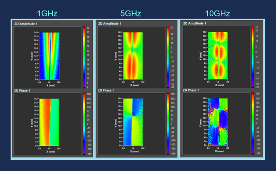
| + | Measurement of electric and magnetic fields has numerous uses and applications in different areas of RF technology. First and foremost, field maps shed light on the physical behavior of RF devices and systems. RF engineers typically use external measurement systems for high frequency characterization. For example, a network analyzer measures the port characteristics of a device. Antennas are usually characterized by their far field radiation patterns. Such external measurements do not reveal much about how signals, fields and waves evolve, build up and propagate inside a device from one port to another, or out into the free space. Just as an oscilloscope probe measures voltages and currents at various points of an electronic circuit, imagine if you could measure electric or magnetic fields at any point inside or around a distributed RF system! That's what NeoScan exactly does for you. | ||
| + | |||
| + | == Non-Invasive Ultra-Near-Field Scanning == | ||
| + | |||
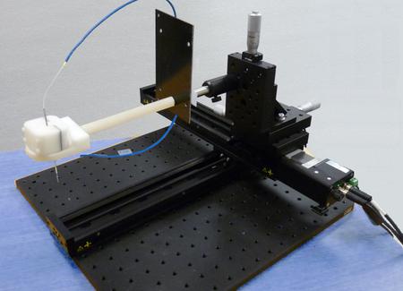
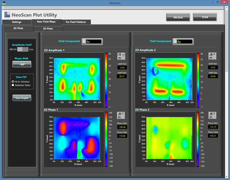
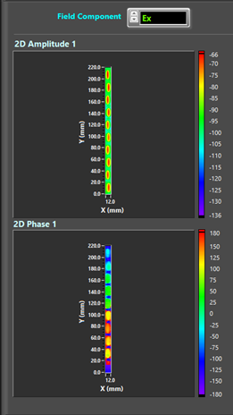
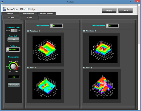
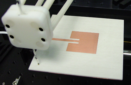
| + | One of the most unique features of the NeoScan system is the very small size of its field probes and the absence of any metallic parts at the probe tip. As a result, you can position a NeoScan field probe very close to the device under test without perturbing the ambient electric or magnetic fields. When mounted on a computer-controlled XY positioner, the probe can scan the surface of your device and create a field map in real time. You can generate maps of the tangential and normal components of the field displaying the amplitude and phase of the respective field components at all the scanned points. | ||
| + | |||
| + | <table> | ||
| + | <tr> | ||
| + | <td> | ||
| + | [[Image:NEOWEB6.png|thumb|550px|Modulating the polarization state of an optical beam passing through an electro-optic crystal.]] | ||
| + | </td> | ||
| + | </tr> | ||
| + | <tr> | ||
| + | <td> | ||
| + | [[Image:NEOWEB14.png|thumb|550px|Modulating the polarization state of an optical beam passing through an electro-optic crystal.]] | ||
| + | </td> | ||
| + | </tr> | ||
| + | </table> | ||
== A Low-Cost Alternative to Costly Anechoic Chambers and Much More... == | == A Low-Cost Alternative to Costly Anechoic Chambers and Much More... == | ||
Revision as of 17:18, 3 December 2015
NON-INVASIVE TURNKEY FIELD MEASUREMENT SYSTEM
Welcome to NeoScan Wiki!
Contents
- 1 Product Overview
- 2 A Unique Test & Evaluation Capability
- 3 Electro-Optic (EO) Effect
- 4 Verification & Validation of Simulation vs. Measurement
- 5 Understanding Your RF Design Through Field Maps
- 6 Non-Invasive Ultra-Near-Field Scanning
- 7 A Low-Cost Alternative to Costly Anechoic Chambers and Much More...
- 8 NeoScan vs. Conventional Near-Field Scanning Systems
- 9 NeoScan: The Perfect Non-Invasive Solution for Diagnostics of High-Power Antenna Systems
- 10 A Unique Technology for Real-Time Detection of Transient Fields & Signals
Product Overview
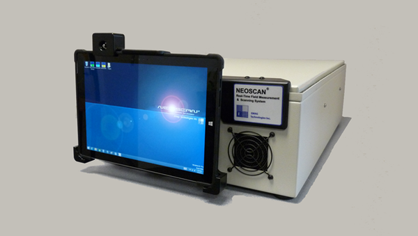
EMAG Technologies Inc. offers the NeoScan family of turnkey field measurement systems. NeoScan systems utilize our unique, patented, electro-optic and magneto-optic probe technologies to detect, sample, measure and scan electric and magnetic fields in a non-invasive manner, while providing a very large operational bandwidth and a very high spatial resolution. NeoScan systems can be used for a variety of RF test and evaluation applications:
- Non-invasive near-field mapping of RF devices, circuits and antennas
- System fault diagnostics through measurement of field emissions, leakage, coupling effects, etc.
- Compact near-field antenna range measurements
- Real time non-contact measurement of fields and signals in a variety of propagation media
NeoScan systems can be customized to meet your most demanding test and evaluation requirements or adapted for various unconventional types of RF measurements. At the present time, EMAG Technologies offers the following four turnkey NeoScan system configurations:
- NeoScan - MSR: Basic NeoScan Field Measurement System.
- NeoScan - MAP: NeoScan Field Mapping System.
- NeoScan - ANT: NeoScan Compact Antenna Characterization System.
- NeoScan - DET: NeoScan Real-Time Field Detection & Capture System.
NeoScan® is a turnkey, electric or magnetic field measurement system. NeoScan systems utilize EMAG's unique, patented, electro-optic (EO) or magneto-optic (MO) field probe technologies. The basic NeoScan system configuration (NeoScan - MSR) uses a non-invasive optical fiber probe to sample and measure the ambient field present at the probe's head. The optical beam from a laser source passes through the optical crystal at the probe head, and its polarization state is modulated by the high frequency electric or magnetic field. The reflected optical beam then passes through an optical processing system and is demodulated. The modulating electric or magnetic field signal is detected by a high frequency photodetector.
In addition to basic field measurement at fixed points in space, NeoScan can also be configured as a near-field scanning system for mapping aperture-level or device-level field distributions with minimal invasiveness to the antenna or device under test. Or it can be used as a real-time field detection system for sensing and detecting electric and magnetic fields in a variety of physical propagation media.
Unlike conventional near-field scanning systems that utilize metallic radiators to pick up the fields, NeoScan probes are absolutely non-metallic, and their operation is based on electro-optic (EO) or magneto-optic (MO) effects. Our field probes feature extremely small EO or MO crystals mounted at the tip of an optical fiber. The combination of small probe size and absence of metallic parts thus leads to the ultimate RF non-invasiveness.
NeoScan provides detailed field maps of passive and active devices and circuits including RFIC's and MMIC's. Such invaluable information can effectively be used for design validation, model verification, fault isolation or performance evaluation of various parts of your RF system.
A Unique Test & Evaluation Capability
Some of the key features of NeoScan field measurement systems include:
- Non-intrusive and non-contact RF measurement thanks to the small footprint and absence of any metal parts or interconnnects at the signal pickup area
- Broad measurement bandwidth (>20GHz) using the same optical probes
- High spatial resolution driven by the laser beam spot size (finer than 100 μm sq)
- Simultaneous amplitude and phase measurement
- Vectorial field measurement with very high cross-polarization suppression
- Very wide dynamic range (>70dB) from very low field intensities under 1V/m to extremely high field intensities above 2MV/m
Electro-Optic (EO) Effect
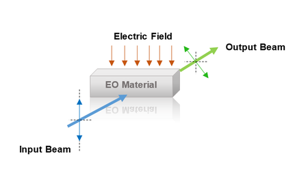
The NeoScan real-time field measurement & scanning system provides an entirely new capability for the measurement of high-intensity electric fields. This technology is based on the Pockel’s effect which measures the phase-retardance of an optical beam due to an impinging electric field. This electro-optic effect is observed in non-centrosymmetric crystals when an electric field is directed along certain crystal axes causes a change in the indices of refraction encountered by an incident optical beam. Figure 1.1 shows the basic principle of the electro-optic effect. The electro-optic effect provides a means of modulating the phase or intensity of the optical radiation. In another sense, this effect also makes it possible to detect the presence of an electric field impinging on the crystal. The polarization of an optical beam travelling through a crystal is altered by the electric field in that crystal. The comparison of polarization states allows determination of the amplitude and phase of the existing RF electric field. Since the electro-optic sensing phenomenon relies on small displacements of the atomic crystal structure, the response time of the process is extremely short. This short response time makes it possible to measure high-frequency electric fields up to the terahertz regime.
A typical EO probe is composed of an optical fiber affixed with an EO crystal coated with a dielectric reflection layer on its bottom surface as shown in Figure 1.2. These probes have very delicate optical interconnects and extreme care must be taken in handling the probes to prevent excessive shock, bending and out of plane stresses.
Due to its broad measurement bandwidth and high spatial resolution, the EO measurement technique is a promising means to characterize RF systems such as microwave and millimeter-wave integrated circuits, HPM sources and systems, and large-scale active arrays and other radiating structures. Unlike the conventional electrical measurement techniques which require some type of metal structure for the resonant detection of an RF signal, NeoScan’s unique real-time EO electric field measurement method requires no metal components. As a result, the field perturbation caused by introducing metal within the vicinity of a device under test (DUT) is significantly reduced.
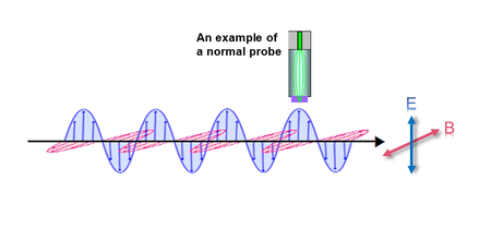
Figure 1.3 shows the electric and magnetic fields distribution of a traveling RF wave with a normal probe shown in typical orientation. To detect the maximum electric field in this configuration, the propagation direction of the optical beam of the probe should be parallel to the E-field direction. In general, a normal EO probe is only sensitive to the electric field component parallel to the probe handle, whereas a tangential probe is sensitive to the electric field component perpendicular to the probe handle. Yet, the E-field sensitivity of a tangential probe depends on its crystal orientation sitting on its tip.
A low noise 1550 nm laser diode is used as optical beam source. The optical connections are fiber-based. The beam is delivered to an optical probe. The polarization of the beam is modulated through an electro-optic crystal on the probe tip. The modulated beam is reflected back into the fiber, and back to the mainframe for analysis. An optical analyzer converts the polarization change of the beam into an amplitude change. The amplitude is linearly proportional to the strength of the external electric field at the probe-crystal location. The equation E=αV is used to calculate the electric field, where α is the calibration factor, or the slope between the electric field E (in V/m) and the measured EO signal V (in V/m/V). For instance, for a calibration factor of 1.082 V/m/V. a measured EO signal of 1000 V (0.001 V), corresponds to and electric field of 1.082 V/m/V 1000 V = 1082 V/m.
Due to the fast response of the EO crystal, it is possible to measure extremely high-bandwidth signals with the normal SNR limitations of wideband signal detection. Using this capability, EMAG Technologies Inc. has developed the world’s first fiber-based real-time polarimetric electric field sensor system – NeoScan – for the measurement of high-power microwave signals. Figure 1.4 is an example of a real time measurement of a 6.6 nsec pulse with 10 kV/m peak field strength. The upper trace shown on the oscilloscope is the received signal, and the lower trace is the detected signal.
The NeoScan system is capable of measuring signals with bandwidths up to 20 GHz and signal levels as low as 1 V/m for optical probes with a 10 m PM fiber. Because the optical probes are free of metallic parts, it is possible to measure extremely high-field strengths since there are no free electron surfaces to generate arcing. The NeoScan can measure fields up at least 2 MV/m and possibly higher.
Verification & Validation of Simulation vs. Measurement
Users of electromagnetic simulation tools often ask a critical question: "How do I know if my simulation results are right and represent the reality?" The primary solutions of most electromagnetic solvers are electric and/or magnetic fields in the given computational domain. All the secondary quantities such as the S/Z/Y parameters, radiation patterns and other characteristics are derived from the primary field quantities. In a similar vein, NeoScan field probes and scanning systems measure the actual electric and magnetic fields at a given point or on a specified surface.
Using these measured field profiles, one can compute all the other secondary quantities of interest. You can use our field maps as an effective means of verification and validation (V&V) of your modeling and simulation tools. Similarly, you can use our electromagnetic analysis tools to verify and validate the field measurement results.
Understanding Your RF Design Through Field Maps
Measurement of electric and magnetic fields has numerous uses and applications in different areas of RF technology. First and foremost, field maps shed light on the physical behavior of RF devices and systems. RF engineers typically use external measurement systems for high frequency characterization. For example, a network analyzer measures the port characteristics of a device. Antennas are usually characterized by their far field radiation patterns. Such external measurements do not reveal much about how signals, fields and waves evolve, build up and propagate inside a device from one port to another, or out into the free space. Just as an oscilloscope probe measures voltages and currents at various points of an electronic circuit, imagine if you could measure electric or magnetic fields at any point inside or around a distributed RF system! That's what NeoScan exactly does for you.
Non-Invasive Ultra-Near-Field Scanning
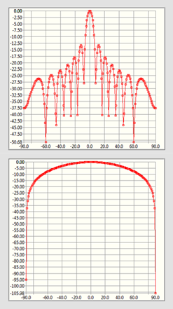
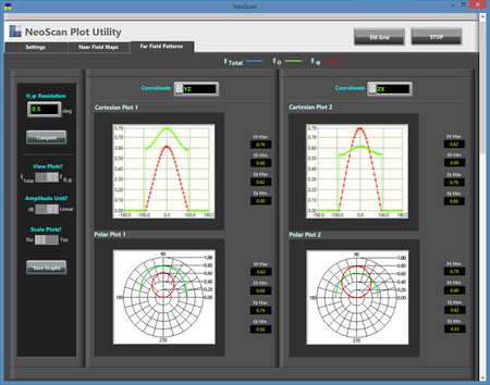
One of the most unique features of the NeoScan system is the very small size of its field probes and the absence of any metallic parts at the probe tip. As a result, you can position a NeoScan field probe very close to the device under test without perturbing the ambient electric or magnetic fields. When mounted on a computer-controlled XY positioner, the probe can scan the surface of your device and create a field map in real time. You can generate maps of the tangential and normal components of the field displaying the amplitude and phase of the respective field components at all the scanned points.
A Low-Cost Alternative to Costly Anechoic Chambers and Much More...
NeoScan systems can be used as an essential tool for characterization, test and evaluation of antennas and phased array systems. The radiation patterns of antennas and arrays are traditionally measured in anechoic chambers. The size of the chamber, its architecture and the quality of the surrounding absorbers all affect the chamber's frequency range of operation and the accuracy of the measured results. Anechoic chamber facilities are very expensive, require a large space and are hard to operate and maintain. Compact near-field ranges are smaller replacements for full-sized chambers.
Near-field scanning systems are by far the most compact alternatives for antenna pattern measurement. Yet, conventional near-field scanning systems have substantial downsides. These systems involve metallic radiators that act as receivers for picking up the near field of the antenna under test (AUT). Such metallic pick-up antennas cannot get close to the AUT since they would perturb its near fields. They also limit the operational bandwidth of the system, and their accuracy degrades significantly at lower frequency bands. Sophisticated software tools are often used in conjunction with these systems to de-embed and minimize various errors due to their specific architectures and configurations.
NeoScan vs. Conventional Near-Field Scanning Systems
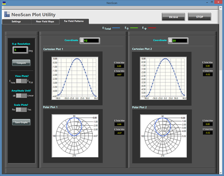
The NeoScan system provides a unique and highly superior alternative to the conventional near-field scanning systems. The NeoScan probes are optical and have absolutely non-metallic compositions. They are extremely small, can get very close to the surface of the radiating aperture, and provide ultra-wideband operation. Due to their non-invasive nature, NeoScan probes can generate ultra-near-field scans of the AUT. These can be used as an invaluable tool for diagnostic purposes. For instance, you can examine the inter-element coupling effects in passive and active phased arrays.
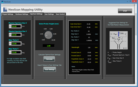
The NeoScan - ANT system comes with an operational software that quickly determines the optimal distance of the probe from the radiating aperture for the fastest scan. The radiation pattern of the AUT is readily computed using a rigorous near-to-far-field transformation without any need for eliminating artifact errors. This is due to the fact that NeoScan measures the "true" near fields of the AUT without any external perturbations.
In short, with NeoScan, you get a compact portable self-contained system that characterizes your antenna system from the very near fields to the very far fields without requiring considerable real estate. NeoScan is particularly useful for phase characterization and calibration large antenna arrays.
NeoScan: The Perfect Non-Invasive Solution for Diagnostics of High-Power Antenna Systems
Characterization of high-power active phased arrays is a very challenging task. Special considerations must be taken into account when measuring high-power antenna systems in an anechoic chamber including operator's safety. NeoScan probes can handle field intensities as large as 2MV/m and can even withstand higher radiated power levels. EMAG's unique probe and optical processing technology allows standoff distances as long as 50 meters between the probe location at the aperture of the high-power array and the optical mainframe and processing unit. This enables you to readily characterize very high-power antenna systems very accurately in a totally non-invasive manner without any serious safety or logistic concerns.
A Unique Technology for Real-Time Detection of Transient Fields & Signals
EMAG Technologies Inc. utilizes a novel patented technology for real-time measurement of electric and magnetic fields. EO and MO modulation effects provide a unique means of sensing and detecting wideband RF and microwave signals in real time. Since the carrier signal is at optical frequencies, the modulating RF field can have substantial bandwidths.
Our probe systems can be used as an instrument for real-time measurement of wideband RF signals in microwave circuits and systems. They can also be utilized in a unique way for a variety of other detection and sensing applications where the presence of metallic parts is highly undesirable such as directed energy and high power microwave systems. Using a robust, patented, optical processing technology, the probes can have standoff distances up to 50 meters from the physical location of the optical mainframe system.
NeoScan systmes can be configured in multi-channel architectures for simultaneous field measurements at multiple points and locations. Different channels can measure different polarizations in a totally coherent manner.
