Difference between revisions of "EM.Libera"
Kazem Sabet (Talk | contribs) (→Excitation Sources) |
Kazem Sabet (Talk | contribs) (→Working with 3D MoM Simulation Data) |
||
| Line 35: | Line 35: | ||
* Click the '''OK''' button of the dielectric material dialog to accept the changes and close it. | * Click the '''OK''' button of the dielectric material dialog to accept the changes and close it. | ||
| − | {{Note|Under dielectric material groups, you cannot draw [[Surface Objects|surface objects]] or [[Curve Objects|[[Curve Objects|[[Curve Objects|curve objects]]]]]].}} | + | {{Note|Under dielectric material groups, you cannot draw [[Surface Objects|surface objects]] or [[Curve Objects|[[Curve Objects|[[Curve Objects|[[Curve Objects|curve objects]]]]]]]].}} |
<table> | <table> | ||
| Line 68: | Line 68: | ||
"Show Mesh" generates a new mesh and displays it if there is none in the memory, or it simply displays an existing mesh in the memory. This is a useful feature because generating a PO mesh may take a long time depending on the complexity and size of objects. If you change the structure or alter the mesh settings, a new mesh is always generated. You can ignore the mesh in the memory and force [[EM.Cube]] to generate a mesh from the ground up by selecting '''Menu > Simulate > Discretization > Regenerate Mesh''' or by right clicking on the '''3-D Mesh''' item of the Navigation Tree and selecting '''Regenerate''' from the contextual menu. | "Show Mesh" generates a new mesh and displays it if there is none in the memory, or it simply displays an existing mesh in the memory. This is a useful feature because generating a PO mesh may take a long time depending on the complexity and size of objects. If you change the structure or alter the mesh settings, a new mesh is always generated. You can ignore the mesh in the memory and force [[EM.Cube]] to generate a mesh from the ground up by selecting '''Menu > Simulate > Discretization > Regenerate Mesh''' or by right clicking on the '''3-D Mesh''' item of the Navigation Tree and selecting '''Regenerate''' from the contextual menu. | ||
| − | To set the PO mesh properties, click on the [[File:mesh_settings.png]] button of the '''Simulate Toolbar''' or select '''Menu > Simulate > Discretization > Mesh Settings... '''or right click on the '''3-D Mesh''' item in the '''Discretization''' section of the Navigation Tree and select '''Mesh Settings...''' from the contextual menu, or use the keyboard shortcut '''Ctrl+G'''. You can change the value of '''Mesh Density''' to generate a triangular mesh with a higher or lower resolutions. Some additional mesh [[parameters]] can be access by clicking the {{key|Tessellation Options}} button of the dialog. In the Tessellation Options dialog, you can change '''Curvature Angle Tolerance''' expressed in degrees, which as a default value of 15°. This parameter can affect the shape of the mesh especially in the case of [[Solid Objects|[[Solid Objects|[[Solid Objects|[[Solid Objects|[[Solid Objects|[[Solid Objects|[[Solid Objects|[[Solid Objects|[[Solid Objects|[[Solid Objects|solid objects]]]]]]]]]]]]]]]]]]]]. It determines the apex angle of the triangular cells of the primary tessellation mesh which is generated initially before cell regularization. Lower values of the angle tolerance result in a less smooth and more pointed mesh of curved surface like a sphere. | + | To set the PO mesh properties, click on the [[File:mesh_settings.png]] button of the '''Simulate Toolbar''' or select '''Menu > Simulate > Discretization > Mesh Settings... '''or right click on the '''3-D Mesh''' item in the '''Discretization''' section of the Navigation Tree and select '''Mesh Settings...''' from the contextual menu, or use the keyboard shortcut '''Ctrl+G'''. You can change the value of '''Mesh Density''' to generate a triangular mesh with a higher or lower resolutions. Some additional mesh [[parameters]] can be access by clicking the {{key|Tessellation Options}} button of the dialog. In the Tessellation Options dialog, you can change '''Curvature Angle Tolerance''' expressed in degrees, which as a default value of 15°. This parameter can affect the shape of the mesh especially in the case of [[Solid Objects|[[Solid Objects|[[Solid Objects|[[Solid Objects|[[Solid Objects|[[Solid Objects|[[Solid Objects|[[Solid Objects|[[Solid Objects|[[Solid Objects|[[Solid Objects|solid objects]]]]]]]]]]]]]]]]]]]]]]. It determines the apex angle of the triangular cells of the primary tessellation mesh which is generated initially before cell regularization. Lower values of the angle tolerance result in a less smooth and more pointed mesh of curved surface like a sphere. |
<table> | <table> | ||
| Line 257: | Line 257: | ||
If the project structure is excited by gap sources, and one or more ports have been defined, the Wire MoM engine calculates the scattering (S) [[parameters]] of the selected ports, all based on the port impedances specified in the project's "Port Definition". If more than one port has been defined in the project, the scattering matrix of the multiport network is calculated. The S [[parameters]] are written into output ASCII data files. Since these data are complex, they are stored as '''.CPX''' files. Every file begins with a header starting with "#". The admittance (Y) and impedance (Z) [[parameters]] are also calculated and saved in complex data files with '''.CPX''' file extensions. The voltage standing wave ratio of the structure at the first port is also computed and saved to a real data '''.DAT''' file. | If the project structure is excited by gap sources, and one or more ports have been defined, the Wire MoM engine calculates the scattering (S) [[parameters]] of the selected ports, all based on the port impedances specified in the project's "Port Definition". If more than one port has been defined in the project, the scattering matrix of the multiport network is calculated. The S [[parameters]] are written into output ASCII data files. Since these data are complex, they are stored as '''.CPX''' files. Every file begins with a header starting with "#". The admittance (Y) and impedance (Z) [[parameters]] are also calculated and saved in complex data files with '''.CPX''' file extensions. The voltage standing wave ratio of the structure at the first port is also computed and saved to a real data '''.DAT''' file. | ||
| − | You can plot the port characteristics from the Navigation Tree. Right click on the '''Port Definition''' item in the '''Observables''' section of the Navigation Tree and select one of the items: '''Plot S [[Parameters]]''', '''Plot Y [[Parameters]]''', '''Plot Z [[Parameters]]''', or '''Plot VSWR''' | + | You can plot the port characteristics from the Navigation Tree. Right click on the '''Port Definition''' item in the '''Observables''' section of the Navigation Tree and select one of the items: '''Plot S [[Parameters]]''', '''Plot Y [[Parameters]]''', '''Plot Z [[Parameters]]''', or '''Plot VSWR'''. |
| − | + | ||
| − | + | ||
| − | + | ||
| − | + | ||
| − | + | ||
| − | + | ||
[[Image:MORE.png|40px]] Click here to learn more about '''[[Data_Visualization_and_Processing#Graphing_Port_Characteristics | Graphing Port Characteristics]]'''. | [[Image:MORE.png|40px]] Click here to learn more about '''[[Data_Visualization_and_Processing#Graphing_Port_Characteristics | Graphing Port Characteristics]]'''. | ||
| Line 308: | Line 302: | ||
3D radiation pattern of the circular loop antenna: (Left) Theta component, (Center) Phi components, and (Right) total far field. | 3D radiation pattern of the circular loop antenna: (Left) Theta component, (Center) Phi components, and (Right) total far field. | ||
| − | |||
| − | |||
| − | |||
| − | |||
| − | |||
| − | |||
| − | |||
| − | |||
| − | |||
| − | |||
| − | |||
| − | |||
| − | |||
| − | |||
| − | |||
| − | |||
| − | |||
| − | |||
=== Computing Radar Cross Section === | === Computing Radar Cross Section === | ||
Revision as of 19:03, 21 July 2015
Contents
An EM.Libera Primer
EM.Libera in a Nutshell
EM.Libera is a 3D free-space structure simulator for modeling metallic and dielectric structures. It features two full-wave Method of Moments (MoM) simulation engines, one based on a Wire MoM formulation and the other based on a Surface MoM formulation. In general, a surface MoM solver is used to simulate your physical structure, which may involve metallic and dielectric objects of arbitrary shapes as well as composite structures that contain joined metal and dielectric regions. If your project workspace contains at least one line or curve object, EM.Libera then invokes its Wire MoM solver. In that case, only metallic structure can be modeled, and all the surface and solid PEC objects are meshed as wireframes.
| |
You can use EM.Libera either for modeling metallic wire objects and wireframe structures or for modeling metallic, dielectric ad composite structures that do not contain lines or curves. |
A Overview of 3D Method Of Moments
The Method of Moments (MoM) is a rigorous, full-wave, numerical technique for solving open boundary electromagnetic problems. Using this technique, you can analyze electromagnetic radiation, scattering and wave propagation problems with relatively short computation times and modest computing resources. The method of moments is an integral equation technique; it solves the integral form of Maxwell’s equations as opposed to their differential forms used in the finite element or finite difference time domain methods.
In a 3D MoM simulation, the currents or fields on the surface of a structure are the unknowns of the problem. The given structure is immersed in the free space. The unknown currents or fields are discretized as a collection of elementary currents or fields with small finite spatial extents. Such elementary currents or fields are called basis functions. They obviously have a vectorial nature and must satisfy Maxwell's equations and relevant boundary conditions individually. The actual currents or fields on the surface of the given structure (the solution of the problem) are expressed as a superposition of these elementary currents or fields with initially unknown amplitudes. Through the MoM solution, you find these unknown amplitudes, from which you can then calculate the currents or fields everywhere in the structure.
EM.Libera offers two distinct 3D MoM simulation engines. The first one is a Wire MoM solver, which is based on Pocklington's integral equation. This solver can be used to simulate wireframe models of metallic structures and is particularly useful for modeling wire-type antennas and arrays. The second engine features a powerful Surface MoM solver. It can model metallic surfaces and solids as well as solid dielectric objects. The Surface MoM solver uses a surface integral equation formulation of Maxwell's equations. In particular, it uses an electric field integral equation (EFIE), magnetic field integral equation (MFIE), or combined field integral equation (CFIE) for modeling PEC regions. For the modeling of the dielectric regions of the physical structure , the so-called Poggio-Miller-Chang-Harrington-Wu-Tsai (PMCHWT) technique is utilized, in which equivalent electric and magnetic currents are assumed on the surface of the dielectric object to formulate the interior and exterior boundary value problems.
![]() Click here to learn more about the theory of 3D Method of Moments.
Click here to learn more about the theory of 3D Method of Moments.
Constructing the Physical Structure & 3D Mesh Generation
Defining Groups Of PEC Objects
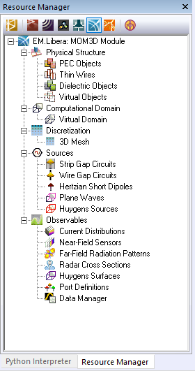
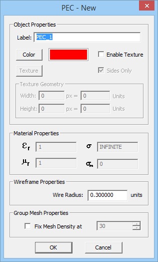
EM.Libera features two different simulation engines: Wire MoM and Surface MoM. Both simulation engines can handle metallic structures. The Wire MoM engine models metallic objects as perfect electric conductor (PEC) wireframe structures, while the Surface MoM engine treats them as PEC surfaces. The PEC objects can be lines, curves, surfaces or solids. All the PEC objects are created under the PEC node in the Physical Structure section of the Navigation Tree. Objects are grouped together by their color. You can insert different PEC groups with different colors. A new PEC group can be defined by simply right clicking on the PEC item in the Navigation Tree and selecting Insert New PEC... from the contextual menu. A dialog for setting up the PEC properties opens up. From this dialog you can change the name of the group or its color. Note that PEC object do not have any material properties that can be edited.
Defining Dielectric Objects
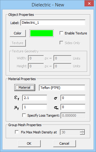
Of EM.Libera's two simulation engines, only the Surface MoM solver can handle dielectric objects. Dielectric objects are created under the Dielectric node in the Physical Structure section of the Navigation Tree. They are grouped together by their color and material properties. You can insert different dielectric groups with different colors and different permittivity er and electric conductivity s. Note that a PEC object is the limiting cases of a lossy dielectric material when σ → ∞.
To define a new Dielectric group, follow these steps:
- Right click on the Dielectric item of the Navigation Tree and select Insert New Dielectric... from the contextual menu.
- Specify a Label, Color (and optional Texture) and the electromagnetic properties of the dielectric material to be created: Relative Permittivity (er) and Electric Conductivity (s).
- You may also choose from a list of preloaded material types. Click the button labeled Material to open EM.Cube's Materials dialog. Select the desired material from the list or type the first letter of a material to find it. For example, typing V selects Vacuum in the list. Once you close the dialog by clicking OK, the selected material properties fill the parameter fields automatically.
- Click the OK button of the dielectric material dialog to accept the changes and close it.
| |
Under dielectric material groups, you cannot draw surface objects or [[Curve Objects|[[Curve Objects|[[Curve Objects|curve objects]]]]]]. |
Moving Objects Between Groups & Modules
By default, the last object group that was defined n the navigation tree is active. The current active group is always listed in bold letters in the navigation tree. All the new objects are inserted under the current active group. A group can be activated by right-clicking on its entry in the navigation tree and then selecting the Active item of the contextual menu. You can move one or more selected objects to any desired PEC group. Right click on the highlighted selection and select Move To ![]() MoM3D
MoM3D ![]() from the contextual menu. This opens another sub-menu with a list of all the available PEC groups already defined in the PO Module. Select the desired PEC group, and all the selected objects will move to that group. The objects can be selected either in the project workspace, or their names can be selected from the Navigation Tree. In the latter case, make sure that you hold the keyboard's Shift Key or Ctrl Key down while selecting a PEC group's name from the contextual menu. In a similar way, you can move one or more objects from a Physical Optics PEC group to EM.CUBE's other modules. In this case, the sub-menus of the Move To
from the contextual menu. This opens another sub-menu with a list of all the available PEC groups already defined in the PO Module. Select the desired PEC group, and all the selected objects will move to that group. The objects can be selected either in the project workspace, or their names can be selected from the Navigation Tree. In the latter case, make sure that you hold the keyboard's Shift Key or Ctrl Key down while selecting a PEC group's name from the contextual menu. In a similar way, you can move one or more objects from a Physical Optics PEC group to EM.CUBE's other modules. In this case, the sub-menus of the Move To ![]() item of the contextual menu will indicate all the EM.CUBE modules that have valid groups for transfer of the select objects.
item of the contextual menu will indicate all the EM.CUBE modules that have valid groups for transfer of the select objects.
3D Mesh Generation
A Note on EM.Libera's Mesh Types
EM.Libera features two simulation engines, Wire MoM and Surface MoM, which require different mesh types. The Wire MoM simulator handles only wire objects and wireframe structures. These objects are discretized as elementary linear elements (filaments). A wire is simply subdivided into smaller segments according to a mesh density criterion. Curved wires are first converted to multi-segment polylines and then subdivided further if necessary. At the connection points between two or more wires, junction basis functions are generated to ensure current continuity.
On the other hands, EM.Libera's Surface MoM solver requires a triangular surface mesh of surface and solid objects.The mesh generating algorithm tries to generate regularized triangular cells with almost equal surface areas across the entire structure. You can control the cell size using the "Mesh Density" parameter. By default, the mesh density is expressed in terms of the free-space wavelength. The default mesh density is 10 cells per wavelength. For meshing surfaces, a mesh density of 7 cells per wavelength roughly translates to 100 triangular cells per squared wavelength. Alternatively, you can base the definition of the mesh density on "Cell Edge Length" expressed in project units.
Creating & Viewing the Mesh
The mesh generation process in EM.Libera involves three steps:
- Setting the mesh properties.
- Generating the mesh.
- Verifying the mesh.
The objects of your physical structure are meshed based on a specified mesh density expressed in cells/λ0. The default mesh density is 10 cells/λ0. To view the PO mesh, click on the ![]() button of the Simulate Toolbar or select Menu > Simulate > Discretization > Show Mesh or use the keyboard shortcut Ctrl+M. When the PO mesh is displayed in the project workspace, EM.Cube's mesh view mode is enabled. In this mode, you can perform view operations like rotate view, pan, zoom, etc. However, you cannot select or move or edit objects. While the mesh view is enabled, the Show Mesh
button of the Simulate Toolbar or select Menu > Simulate > Discretization > Show Mesh or use the keyboard shortcut Ctrl+M. When the PO mesh is displayed in the project workspace, EM.Cube's mesh view mode is enabled. In this mode, you can perform view operations like rotate view, pan, zoom, etc. However, you cannot select or move or edit objects. While the mesh view is enabled, the Show Mesh ![]() button remains depressed. To get back to the normal view or select mode, click this button one more time, or deselect Menu > Simulate > Discretization > Show Mesh to remove its check mark or simply click the Esc Key of the keyboard.
button remains depressed. To get back to the normal view or select mode, click this button one more time, or deselect Menu > Simulate > Discretization > Show Mesh to remove its check mark or simply click the Esc Key of the keyboard.
"Show Mesh" generates a new mesh and displays it if there is none in the memory, or it simply displays an existing mesh in the memory. This is a useful feature because generating a PO mesh may take a long time depending on the complexity and size of objects. If you change the structure or alter the mesh settings, a new mesh is always generated. You can ignore the mesh in the memory and force EM.Cube to generate a mesh from the ground up by selecting Menu > Simulate > Discretization > Regenerate Mesh or by right clicking on the 3-D Mesh item of the Navigation Tree and selecting Regenerate from the contextual menu.
To set the PO mesh properties, click on the ![]() button of the Simulate Toolbar or select Menu > Simulate > Discretization > Mesh Settings... or right click on the 3-D Mesh item in the Discretization section of the Navigation Tree and select Mesh Settings... from the contextual menu, or use the keyboard shortcut Ctrl+G. You can change the value of Mesh Density to generate a triangular mesh with a higher or lower resolutions. Some additional mesh parameters can be access by clicking the Tessellation Options button of the dialog. In the Tessellation Options dialog, you can change Curvature Angle Tolerance expressed in degrees, which as a default value of 15°. This parameter can affect the shape of the mesh especially in the case of [[Solid Objects|[[Solid Objects|[[Solid Objects|[[Solid Objects|[[Solid Objects|[[Solid Objects|[[Solid Objects|[[Solid Objects|[[Solid Objects|[[Solid Objects|solid objects]]]]]]]]]]]]]]]]]]]]. It determines the apex angle of the triangular cells of the primary tessellation mesh which is generated initially before cell regularization. Lower values of the angle tolerance result in a less smooth and more pointed mesh of curved surface like a sphere.
button of the Simulate Toolbar or select Menu > Simulate > Discretization > Mesh Settings... or right click on the 3-D Mesh item in the Discretization section of the Navigation Tree and select Mesh Settings... from the contextual menu, or use the keyboard shortcut Ctrl+G. You can change the value of Mesh Density to generate a triangular mesh with a higher or lower resolutions. Some additional mesh parameters can be access by clicking the Tessellation Options button of the dialog. In the Tessellation Options dialog, you can change Curvature Angle Tolerance expressed in degrees, which as a default value of 15°. This parameter can affect the shape of the mesh especially in the case of [[Solid Objects|[[Solid Objects|[[Solid Objects|[[Solid Objects|[[Solid Objects|[[Solid Objects|[[Solid Objects|[[Solid Objects|[[Solid Objects|[[Solid Objects|solid objects]]]]]]]]]]]]]]]]]]]]. It determines the apex angle of the triangular cells of the primary tessellation mesh which is generated initially before cell regularization. Lower values of the angle tolerance result in a less smooth and more pointed mesh of curved surface like a sphere.
Mesh of Connected Objects
All the objects belonging to the same PEC or dielectric group are merged together using the Boolean union operation before meshing. If your structure contains attached, interconnected or overlapping solid objects, their internal common faces are removed and only the surface of the external faces is meshed. Similarly, all the surface objects belonging to the same PEC group are merged together and their internal edges are removed before meshing. Note that a solid and a surface object belonging to the same PEC group might not always be merged properly.
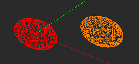
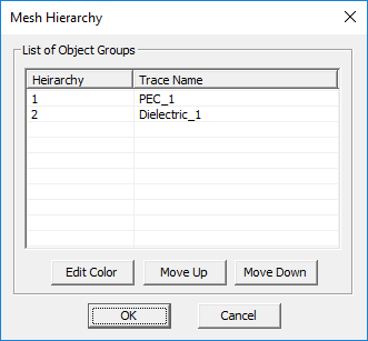
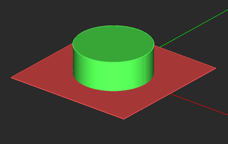
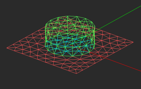
When two objects belonging to two different material groups overlap or intersect each other, EM.Libera has to determine how to designate the overlap or common volume or surface. As an example, the figure below shows a dielectric cylinder sitting on top of a PEC plate. The two object share a circular area at the base of the cylinder. Are the cells on this circle metallic or do they belong to the dielectric material group? Note that the cells of the junction are displayed in a different color then those of either groups. To address problems of this kind, EM.Libera does provide a "Material Hierarchy" table, which you can modify. To access this table, select Menu > Simulate < discretization < Mesh Hierarchy.... The PEC groups by default have the highest priority and reside at the top of the table. You can select an group from the table and change its hierarch using the Move Up or Move Down buttons of the dialog. You can also change the color of junction cells that belong to each group.
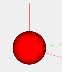
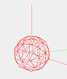
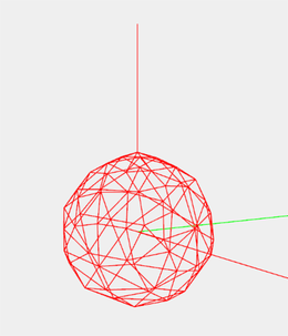
You can connect a line object to a touching surface. To connect lines to surfaces and allow for current continuity, you must make sure that the box labeled Connect Lines to Touching Surfaces is checked in the Mesh Settings Dialog. If the end of a line lies on a flat surface, EM.CUBE will detect that and create the connection automatically. However, this may not always be the case if the surface is not flat and has curvature. In such cases, you have to specifically instruct EM.CUBE to enforce the connection. An example of this case is shown in the figure below.
The line object at the top of a PEC sphere and the structure's mesh without and with proximity mesh connection enforced.
Excitation Sources
Gaps Sources On Wires
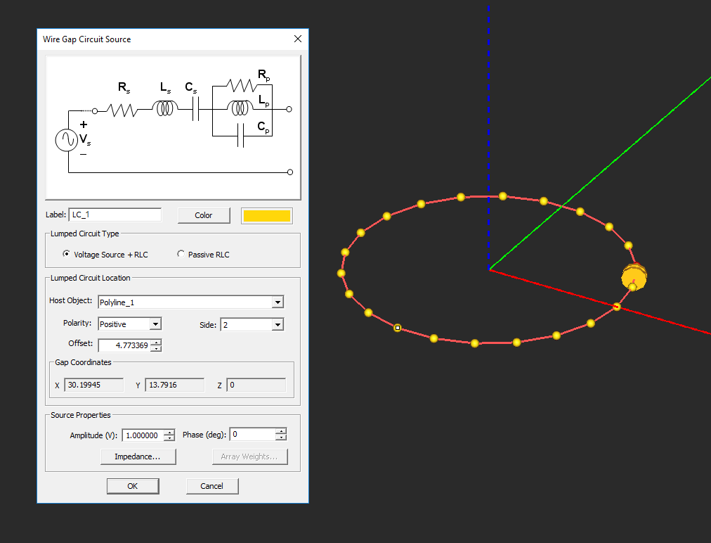
A Gap is an infinitesimally narrow discontinuity that is placed on the path of the current. In EM.Cube's MoM3D Module, a gap is used to define an excitation source in the form of an ideal voltage source. Gap sources can be placed only on Line and Polyline objects. If you want to excite a curved wire antennas such as a circular loop or helix with a gap source, first you have to convert the curve object into a polyline using EM.Cube's Polygonize Tool. The gap splits the wire into two segment with a an infinitesimally small spacing between them, across which the ideal voltage source is connected. To define a new gap source, follow these steps:
- Right click on the Gap Sources item in the Sources section of the Navigation Tree and select Insert New Source... from the contextual menu. The Gap Source Dialog opens up.
- In the Source Location section of the dialog, you will find a list of all the line and polyline objects in the Project Workspace. Select the desired line or polyline object. A gap symbol is immediately placed on the selected object.
- The box labeled Direction shows the polarity of the voltage source placed on the selected object. You have the option to select either the positive or negative direction for the source. This parameter is obviously relevant only for lumped elements of active type.
- In the case of a gap on a line object, in the box labeled Offset, enter the distance of the source from the start point of the line. This value by default is initially set to the center of the line object.
- In the case of a gap on a polyline object, first choose the Side of the polyline where you want to place the source. Then, in the box labeled Offset, enter the distance of the source from the start point of that side. By default, a gap source is placed at the center of the first side of the polyline object. You can also change the offset value using the spin buttons. If you keep pushing the spin buttons, the gap source moves from one side to the next, and its side index and offset value are adjusted automatically.
- In the Source Properties section, you can specify the Source Amplitude in Volts and the Phase in Degrees.
A gap source placed on one side of a polyline representing a polygonized circular loop.
![]() Click here to learn more about Using Sources & Loads in Antenna Arrays.
Click here to learn more about Using Sources & Loads in Antenna Arrays.
Modeling Lumped Circuits
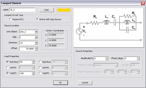
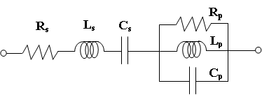
In EM.Cube's MoM3D Module, you can define simple lumped elements in a similar manner as gap sources. In fact, a lumped element is equivalent to an infinitesimally narrow gap that is placed in the path of the current, across which Ohm's law is enforced as a boundary condition. You can define passive RLC lumped elements or active lumped elements containing a voltage gap source. The latter case can be used to excite a wire structure and model a non-ideal voltage source with an internal resistance. Unlike the FDTD Module's single-device lumped loads that connect between two adjacent nodes, the MoM3D Module's lumped circuit represent a series-parallel combination of resistor, inductor and capacitor elements. This is shown in the figure below:
To define a new lumped element, follow these steps:
- Right click on the Lumped Elements item in the Sources section of the Navigation Tree and select Insert New Source... from the contextual menu. The Lumped Element Dialog opens up.
- In the Lumped Circuit Type select one of the two options: Passive RLC or Active with Gap Source. Choosing the latter option enables the Source Properties section of the dialog.
- In the Source Location section of the dialog, you will find a list of all the line and polyline objects in the Project Workspace. Select the desired line or polyline object. A lumped element symbol is immediately placed on the selected object.
- The box labeled Direction shows the polarity of the voltage source placed on the selected object. You have the option to select either the positive or negative direction for the source.
- In the case of a gap on a line object, in the box labeled Offset, enter the distance of the source from the start point of the line. This value by default is initially set to the center of the line object.
- In the case of a gap on a polyline object, first choose the Side of the polyline where you want to place the source. Then, in the box labeled Offset, enter the distance of the source from the start point of that side. By default, a gap source is placed at the center of the first side of the polyline object. You can also change the offset value using the spin buttons. If you keep pushing the spin buttons, the gap source moves from one side to the next, and its side index and offset value are adjusted automatically.
- In the Load Properties section, the series and shunt resistance values Rs and Rp are specified in Ohms, the series and shunt inductance values Ls and Lp are specified in nH (nanohenry), and the series and shunt capacitance values Cs and Cp are specified in pF (picofarad). The impedance of the circuit is calculated at the operating frequency of the project. Only the elements that have been checked are taken into account. By default, only the series resistor has a value of 50Σ and all other circuit elements are initially grayed out.
- If the lumped element is active and contains a gap source, the Source Properties section of the dialog becomes enabled. Here you can specify the Source Amplitude in Volts (or in Amperes in the case of PMC traces) and the Phase in degrees.
- If the workspace contains an array of line or polyline objects, the array object will be listed as an eligible object for gap source placement. A lumped element will be placed on each element of the array. All the lumped elements will have identical direction, offset, resistance, inductance and capacitance values. If you define an active lumped element, you can prescribe certain amplitude and/or phase distribution to the gap sources. The available amplitude distributions include Uniform, Binomial and Chebyshev. In the last case, you need to set a value for minimum side lobe level (SLL) in dB. You can also define Phase Progression in degrees along all three principal axes.
Defining Ports
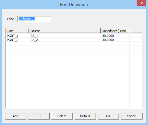
Ports are used to order and index gap sources for S parameter calculation. They are defined in the Observables section of the Navigation Tree. Right click on the Port Definition item of the Navigation Tree and select Insert New Port Definition... from the contextual menu. The Port Definition Dialog opens up, showing the total number of existing sources in the workspace. By default, as many ports as the total number of sources are created. You can define any number of ports equal to or less than the total number of sources. This includes both gap sources and active lumped elements (which contain gap sources). In the Port Association section of this dialog, you can go over each one of the sources and associate them with a desired port. Note that you can associate more than one source with same given port. In this case, you will have a coupled port. All the coupled sources are listed as associated with a single port. However, you cannot associate the same source with more than one port. Finally, you can assign Port Impedance in Ohms. By default, all port impedances are 50Σ. The table titled Port Configuration lists all the ports and their associated sources and port impedances.
| |
In EM.Cube you cannot assign ports to an array object, even if it contains sources on its elements. To calculate the S parameters of an antenna array, you have to construct it using individual elements, not as an array object. |
The MoM3D Module's port definition dialog.
Hertzian Dipole Sources
A short dipole provides a simple way of exciting a structure in the MoM3D Module. A short dipole source acts like an infinitesimally small ideal current source. To define a short dipole source, follow these steps:
- Right click on the Short Dipoles item in the Sources section of the Navigation Tree and select Insert New Source... from the contextual menu. The Short Dipole dialog opens up.
- In the Source Location section of the dialog, you can set the coordinate of the center of the short dipole. By default, the source is placed at the origin of the world coordinate system at (0,0,0).You can type in new coordinates or use the spin buttons to move the dipole around.
- In the Source Properties section, you can specify the Amplitude in Volts, the Phase in degrees as well as the Length of the dipole in project units.
- In the Direction Unit Vector section, you can specify the orientation of the short dipole by setting values for the components uX, uY, and uZ of the dipole's unit vector. The default values correspond to a vertical (Z-directed) short dipole. The dialog normalizes the vector components upon closure even if your component values do not satisfy a unit magnitude.
When you simulate a wire structure in the MoM3D Module, you can define a Current Distribution Observable in your project. This is used not only to visualize the current distribution in the project workspace but also to save the current solution into an ASCII data file. This data file is called "MoM.IDI" by default and has a .IDI file extension. The current data are saved as line segments representing each of the wire cells together with the complex current at the center of each cell. In the MoM3D Module, you can import the current data from an existing .IDI file to serve as a set of short dipoles for excitation. To import a wire current solution, right click on Short Dipoles item in the Sources section of the Navigation Tree and select Import Dipole Source... from the contextual menu. This opens up the standard Windows Open dialog with the file type set to .IDI. Browse your folders to find the right current data file. Once you find it, select it and click the Open button of the dialog. This will create as many short dipole sources on the PO Module's Navigation Tree as the total number of mesh cells in the Wire MoM solution. From this point on, each of the imported dipoles behave like a regular short dipole source. You can open the property dialog of each individual source and modify its parameters.
Plane Wave Sources
The wire-frame structure in the MoM3D Module can be excited by an incident plane wave. In particular, a plane wave source can be used to compute the radar cross section of a metallic target. A plane wave is defined by its propagation vector indicating the direction of incidence and its polarization. EM.CUBE's MoM3D Module provides the following polarization options:
- TMz
- TEz
- Custom Linear
- LCPz
- RCPz
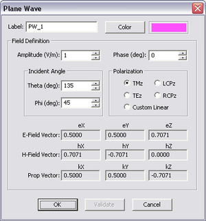
The direction of incidence is defined through the θ and φ angles of the unit propagation vector in the spherical coordinate system. The values of these angles are set in degrees in the boxes labeled Theta and Phi. The default values are θ = 180° and φ = 0° representing a normally incident plane wave propagating along the -Z direction with a +X-polarized E-vector. In the TMz and TEz polarization cases, the magnetic and electric fields are parallel to the XY plane, respectively. The components of the unit propagation vector and normalized E- and H-field vectors are displayed in the dialog. In the more general case of custom linear polarization, besides the incidence angles, you have to enter the components of the unit electric Field Vector. However, two requirements must be satisfied: ê . ê = 1 and ê × k = 0 . This can be enforced using the Validate button at the bottom of the dialog. If these conditions are not met, an error message is generated. The left-hand (LCP) and right-hand (RCP) circular polarization cases are restricted to normal incidences only (θ = 180°).
To define a plane wave source follow these steps:
- Right click on the Plane Waves item in the Sources section of the Navigation Tree and select Insert New Source... The Plane wave Dialog opens up.
- In the Field Definition section of the dialog, you can enter the Amplitude of the incident electric field in V/m and its Phase in degrees. The default field Amplitude is 1 V/m with a zero Phase.
- The direction of the Plane Wave is determined by the incident Theta and Phi angles in degrees. You can also set the Polarization of the plane wave and choose from the five options described earlier. When the Custom Linear option is selected, you also need to enter the X, Y, Z components of the E-Field Vector.
| |
In the spherical coordinate system, normal plane wave incidence from the top of the domain downward corresponds to θ of 180°. |
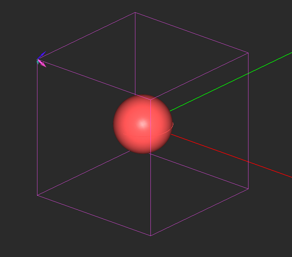
Figure: Illuminating a metallic sphere with an obliquely incident plane wave source.
Running Wire MoM Simulations
Running A Wire MoM Analysis

Once you have set up your metal structure in EM.CUBE's MoM3D Module, have defined sources and observables and have examined the quality of the structure's wire-frame mesh, you are ready to run a simulation. To open the Run Simulation Dialog, click the Run ![]() button of the Compute Toolbar or select Menu
button of the Compute Toolbar or select Menu ![]() Compute
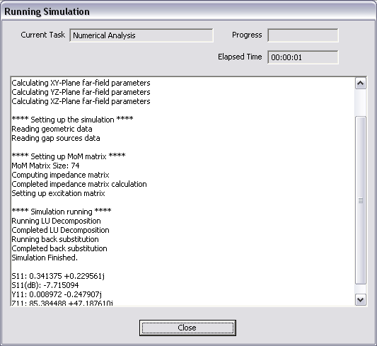
Compute ![]() Run...or use the keyboard shortcut Ctrl+R. To start the simulation click the Run button of this dialog. Once the Wire MoM simulation starts, a new dialog called Output Window opens up that reports the various stages of Wire MoM simulation, displays the running time and shows the percentage of completion for certain tasks during the Wire MoM simulation process. A prompt announces the completion of the Wire MoM simulation. At this time, EM.CUBE generates a number of output data files that contain all the computed simulation data. These include current distributions, near field data, far field radiation pattern data as well bi-static or mono-static radar cross sections (RCS) if the structure is excited by a plane wave source.
Run...or use the keyboard shortcut Ctrl+R. To start the simulation click the Run button of this dialog. Once the Wire MoM simulation starts, a new dialog called Output Window opens up that reports the various stages of Wire MoM simulation, displays the running time and shows the percentage of completion for certain tasks during the Wire MoM simulation process. A prompt announces the completion of the Wire MoM simulation. At this time, EM.CUBE generates a number of output data files that contain all the computed simulation data. These include current distributions, near field data, far field radiation pattern data as well bi-static or mono-static radar cross sections (RCS) if the structure is excited by a plane wave source.
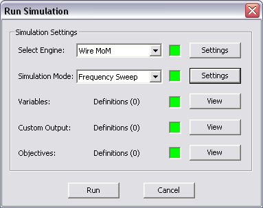
You have the choice to run a Fixed Frequency simulation, which is the default choice, or run a Frequency Sweep. In the former case, the simulation will be carried out at the Center Frequency of the project. This frequency can be changed from the Frequency Dialog of the project or you can click the Frequency Settings button of the Run Dialog to open up the Frequency Settings dialog. You can change the value of Center Frequency from this dialog, too.
In case you choose Frequency Sweep, the Frequency Settings dialog gives two options for Sweep Type: Adaptive or Uniform. In a uniform sweep, equally spaced samples of the frequency are used between the Start and End frequencies. These are initially set by the project Bandwidth, but you can change their values from the Frequency Settings dialog. The default Number of Samples is 10.In the case of adaptive sweep, you have to specify the Maximum Number of Iterations as well as the Error. An adaptive sweep simulation starts with a few initial frequency samples, where the Wire MoM engine is run. Then, the intermediary samples are calculated in a progressive manner. At each iteration, the frequency samples are used to calculate a rational approximation of the S parameter response over the specified frequency range. The process stops when the error criterion is met.
Figure: The output window.
Setting Wire MoM Numerical Parameters
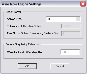
A Wire MoM simulation involves a number of numerical parameters that normally take default values unless you change them. You can access these parameters and change their values by clicking on the Settings button next to the "Select Engine" drop-down list in the Run Dialog. This opens up the Wire MoM Engine Settings Dialog. In the Solver section of the dialog, you can choose the type of linear solver. The current options are LU and Bi-Conjugate Gradient (BiCG). The LU solver is a direct solver and is the default option of the MoM3D Module. The BiCG solver is iterative. Once selected, you have to set a Tolerance for its convergence. You can also change the maximum number of BiCG iterations by setting a new value for Max. No. of Solver Iterations / System Size. The Wire MoM simulator is based on Pocklington's integral equation method. In this method, the wires are assumed to have a very small radius. The basis functions are placed on the axis of the "wire cylinder", while the Galerkin testing is carried out on its surface to avoid the singularity of the Green's functions. In the "Source Singularity" section of the dialog, you can specify the Wire Radius . EM.CUBE's MoM3D Module assumes an identical wire radius for all wires and wireframe structures. This radius is expressed in free space wavelengths and its default value is 0.001λ0. The value of the wire radius has a direct influence on the wire's computed reactance.
The wire MoM engine settings dialog.
3D MoM Sweep Simulations
You can run EM.CUBE's MoM3D simulation engine in the sweep mode, whereby a parameter like frequency, plane wave angles of incidence or a user defined variable is varied over a specified range at predetermined samples. The output data are saved into data file for visualization and plotting. EM.CUBE's MoM3D Module currently offers three types of sweep:
- Frequency Sweep
- Angular Sweep
- Parametric Sweep
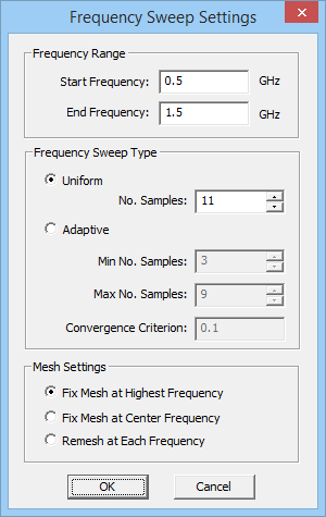
To run a MoM3D sweep, open the Run Simulation Dialog and select one of the above sweep types from the Simulation Mode drop-down list in this dialog. If you select either frequency or angular sweep, the Settings button located next to the simulation mode drop-down list becomes enabled. If you click this button, the Frequency Settings Dialog or Angle Settings Dialog opens up, respectively. In the frequency settings dialog, you can set the start and end frequencies as well as the number of frequency samples. The start and end frequency values are initially set based on the project's center frequency and bandwidth. During a frequency sweep, as the project's frequency changes, so does the wavelength. As a result, the mesh of the structure also changes at each frequency sample. The frequency settings dialog gives you three choices regarding the mesh of the project structure during a frequency sweep:
- Fix mesh at the highest frequency.
- Fix mesh at the center frequency.
- Re-mesh at each frequency.
The MoM3D Module offers two types of frequency sweep: adaptive or uniform. In a uniform sweep, equally spaced frequency samples are generated between the start and end frequencies. In the case of an adaptive sweep, you must specify the Maximum Number of Iterations as well as the Error. An adaptive sweep simulation starts with a few initial frequency samples, where the Wire MoM engine is initially run. Then, the intermediary frequency samples are calculated and inserted in a progressive manner. At each iteration, the frequency samples are used to calculate a rational approximation of the scattering parameter response over the specified frequency range. The process stops when the specified error criterion is met in a mean-square sense. The adaptive sweep simulation results are always continuous and smooth. This is due to the fact that a rational function curve is fitted through the discrete frequency data points. This usually captures frequency response characteristics such as resonances with much fewer calculated data points. However, you have to make sure that the process converges. Otherwise, you might get an entirely wrong, but still perfectly smooth, curve at the end of the simulation.
The MoM3D Module's run simulation dialog with frequency sweep selected and the frequency settings dialog.
In a parametric sweep, one or more user defined variables are varied at the same time over their specified ranges. This creates a parametric space with the total number of samples equal to the product of the number of samples for each variable. The user defined variables are defined using EM.CUBE's Variables Dialog. For a description of EM.CUBE variables, please refer to the CUBECAD manual or the "Parametric Sweep" sections of the FDTD or Planar Module manuals.
Working with 3D MoM Simulation Data
Visualizing Wire Current Distributions

At the end of a MoM3D simulation, EM.CUBE's Wire MoM engine generates a number of output data files that contain all the computed simulation data. The main output data are the current distributions and far fields. You can easily examine the 3-D color-coded intensity plots of current distributions in the Project Workspace. Current distributions are visualized on all the wires and the magnitude and phase of the electric currents are plotted for all the PEC objects. In order to view these currents, you must first define current sensors before running the Wire MoM simulation. To do this, right click on the Current Distributions item in the Observables section of the Navigation Tree and select Insert New Observable.... The Current Distribution Dialog opens up. Accept the default settings and close the dialog. A new current distribution node is added to the Navigation Tree. Unlike the Planar Module, in the MoM3D Module you can define only one current distribution node in the Navigation Tree, which covers all the PEC object in the Project Workspace. After a Wire MoM simulation is completed, new plots are added under the current distribution node of the Navigation Tree. Separate plots are produced for the magnitude and phase of the linear wire currents. The magnitude maps are plotted on a normalized scale with the minimum and maximum values displayed in the legend box. The phase maps are plotted in radians between -π and π.
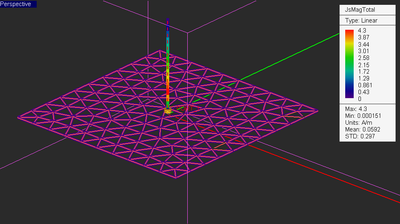
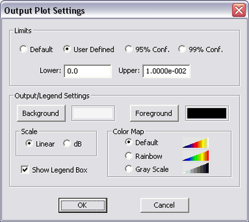
Current distribution maps are displayed with some default settings and options. You can customize the individual maps (total, magnitude, phase, etc.). To do so, open the Output Plot Settings Dialog by right clicking on the specific plot entry in the Navigation Tree and selecting Properties... or by double clicking on the surface of the plot's legend box. Two scale options are available: Linear and dB. With the Linear (default) option selected, the current value is always normalized to the maximum total current in that plane, and the normalized scale is mapped between the minimum and maximum values. If the dB option is selected, the normalized current is converted to dB scale. The plot limits (bounds) can be set individually for every current distribution plot. In the Limits section of the plot's property dialog, you see four options: Default, User Defined, 95% Conf. and 95% Conf.. Select the user defined option and enter new values for the Lower and Upper limits. The last two options are used to remove the outlier data within the 95% and 99% confidence intervals, respectively. In other words, the lower and upper limits are set to ? ± 1.96? and ? ± 2.79? , respectively, assuming a normal distribution of the data. Three color maps are offered: Default, Rainbow and Grayscale. You can hide the legend box by deselecting the box labeled Show Legend Box. You can also change the foreground and background colors of the legend box.
![]() Click here to learn more about Visualizing 3D Current Distribution Maps.
Click here to learn more about Visualizing 3D Current Distribution Maps.
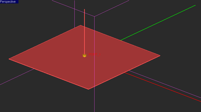
Figure: A monopole antenna connected above a PEC plate and its current distribution with the default plot settings.
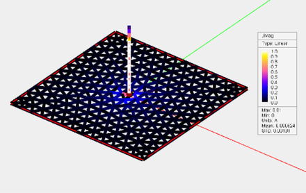
Figure: The output plot settings dialog, and the current distribution of the monopole-plate structure with a user defined upper limit.
Scattering Parameters and Port Characteristics
If the project structure is excited by gap sources, and one or more ports have been defined, the Wire MoM engine calculates the scattering (S) parameters of the selected ports, all based on the port impedances specified in the project's "Port Definition". If more than one port has been defined in the project, the scattering matrix of the multiport network is calculated. The S parameters are written into output ASCII data files. Since these data are complex, they are stored as .CPX files. Every file begins with a header starting with "#". The admittance (Y) and impedance (Z) parameters are also calculated and saved in complex data files with .CPX file extensions. The voltage standing wave ratio of the structure at the first port is also computed and saved to a real data .DAT file.
You can plot the port characteristics from the Navigation Tree. Right click on the Port Definition item in the Observables section of the Navigation Tree and select one of the items: Plot S Parameters, Plot Y Parameters, Plot Z Parameters, or Plot VSWR.
![]() Click here to learn more about Graphing Port Characteristics.
Click here to learn more about Graphing Port Characteristics.
Near Field Visualization

EM.CUBE allows you to visualize the near fields at a specific field sensor plane. Calculation of near fields is a post-processing process and may take a considerable amount of time depending on the resolution that you specify. To define a new Field Sensor, follow these steps:
- Right click on the Field Sensors item in the Observables section of the Navigation Tree and select Insert New Observable...
- The Label box allows you to change the sensor’s name. you can also change the color of the field sensor plane using the Color button.
- Set the Direction of the field sensor. This is specified by the normal vector of the sensor plane. The available options are X, Y and Z, with the last being the default option.
- By default EM.CUBE creates a field sensor plane passing through the origin of coordinates (0,0,0) and coinciding with the XY plane. You can change the location of the sensor plane to any point by typing in new values for the X, Y and Z Center Coordinates. You can also changes these coordinates using the spin buttons. Keep in mind that you can move a sensor plane only along the specified direction of the sensor. Therefore, only one coordinate can effectively be changed. As you increment or decrement this coordinate, you can observe the sensor plane moving along that direction in the Project Workspace.
- The initial size of the sensor plane is 100 × 100 project units. You can change the dimensions of the sensor plane to any desired size. You can also set the Number of Samples along the different directions. These determine the resolution of near field calculations. Keep in mind that large numbers of samples may result in long computation times.
After closing the Field Sensor Dialog, the a new field sensor item immediately appears under the Observables section in the Navigation Tree and can be right clicked for additional editing. Once a Wire MoM simulation is finished, a total of 14 plots are added to every field sensor node in the Navigation Tree. These include the magnitude and phase of all three components of E and H fields and the total electric and magnetic field values. Click on any of these items and a color-coded intensity plot of it will be visualized on the Project Workspace. A legend box appears in the upper right corner of the field plot, which can be dragged around using the left mouse button. The values of the magnitude plots are normalized between 0 and 1. The legend box contains the minimum field value corresponding to 0 of the color map, maximum field value corresponding to 1 of the color map, and the unit of the field quantity, which is V/m for E-field and A/m for H-field. The values of phase plots are always shown in Radians between -π and π. You can change the view of the field plot with the available view operations such as rotating, panning, zooming, etc.
![]() Click here to learn more about Visualizing 3D Near Field Maps.
Click here to learn more about Visualizing 3D Near Field Maps.
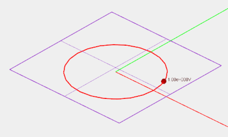
Figure: A circular loop antenna fed by a gap source.
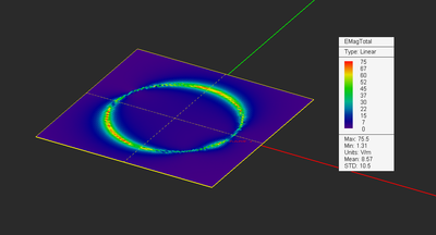
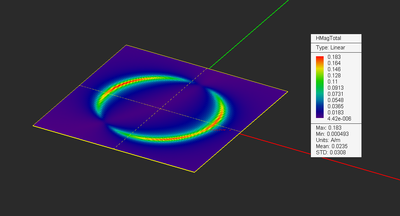
Electric and magnetic field plots of the circular loop antenna.
Visualizing 3D Radiation Patterns

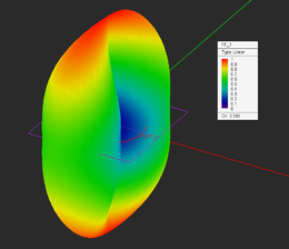
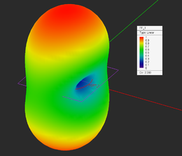
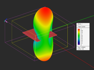
Unlike the FDTD method, the method of moments does not need a far field box to perform near-to-far-field transformations. But you still need to define a far field observable if you want to plot radiation patterns in EM.Libera. A far field can be defined by right clicking on the Far Fields item in the Observables section of the Navigation Tree and selecting Insert New Radiation Pattern... from the contextual menu. The Radiation Pattern dialog opens up. You can accept most of the default settings in this dialog. The Output Settings section allows you to change the Angle Increment for both Theta and Phi observation angles in the degrees. These parameters indeed set the resolution of far field calculations. The default values are 5 degrees. After closing the radiation pattern dialog, a far field entry immediately appears with its given name under the Far Fields item of the Navigation Tree and can be right clicked for further editing. After a 3D MoM simulation is finished, three radiation patterns plots are added to the far field entry in the Navigation Tree. These are the far field component in Theta direction, the far field component in Phi direction and the total far field.
![]() Click here to learn more about the theory of Far Field Computations.
Click here to learn more about the theory of Far Field Computations.
![]() Click here to learn more about the theory of Using Array Factors to Model Antenna Arrays .
Click here to learn more about the theory of Using Array Factors to Model Antenna Arrays .
![]() Click here to learn more about Visualizing 3D Radiation Patterns.
Click here to learn more about Visualizing 3D Radiation Patterns.
![]() Click here to learn more about Plotting 2D Radiation Graphs.
Click here to learn more about Plotting 2D Radiation Graphs.
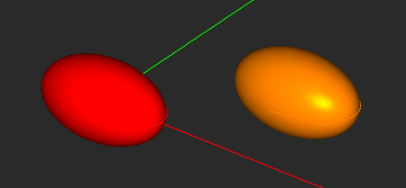
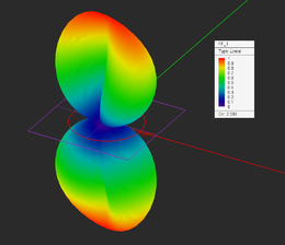
3D radiation pattern of the circular loop antenna: (Left) Theta component, (Center) Phi components, and (Right) total far field.
Computing Radar Cross Section

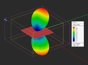
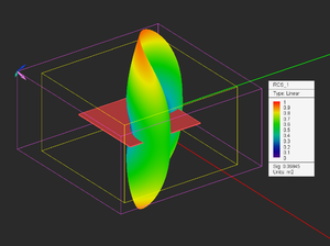
When your structure is excited by a plane wave source, the calculated far field data indeed represent the scattered fields. EM.Libera can calculate the radar cross section (RCS) of a target. Three RCS quantities are computed: the φ and θ components of the radar cross section as well as the total radar cross section: σθ, σφ, and σtot. In addition, EM.Libera calculates two types of RCS for each structure: Bi-Static RCS and Mono-Static RCS. In bi-static RCS, the structure is illuminated by a plane wave at incidence angles θ0 and φ0 and the RCS is measured and plotted at all θ and φ angles. In mono-static RCS, the structure is illuminated by a plane wave at incidence angles θ0 and φ0 and the RCS is measured and plotted at the echo angles 180°-θ0 and φ0.It is clear that in the case of mono-static RCS, the Wire MoM simulation engine runs an internal angular sweep, whereby the values of the plane wave incidence angles θ0 and φ0 are varied over the intervals [0°, 180°] and [0°, 360°], respectively, and the backscatter RCS is recorded.
To calculate RCS, first you have to define an RCS observable instead of a radiation pattern. Right click on the Far Fields item in the Observables section of the Navigation Tree and select Insert New RCS... to open the Radar Cross Section Dialog. Use the Label box to change the name of the far field or change the color of the far field box using the Color button. Select the type of RCS from the two radio buttons labeled Bi-Static RCS and Mono-Static RCS. The former is the default choice. The resolution of RCS calculation is specified by Angle Increment expressed in degrees. By default, the θ and φ angles are incremented by 5 degrees. At the end of a Wire MoM simulation, besides calculating the RCS data over the entire (spherical) 3-D space, a number of 2-D RCS graphs are also generated. These are RCS cuts at certain planes, which include the three principal XY, YZ and ZX planes plus one additional constant φ-cut. This latter cut is at φ=45° by default. You can assign another phi angle in degrees in the box labeled Non-Principal Phi Plane.
At the end of a Wire MoM simulation, the thee RCS plots σθ, σφ, and σtotare added under the far field section of the navigation tree. The 2D RCS graphs can be plotted from the data manager exactly in the same way that you plot 2D radiation pattern graphs. A total of eight 2D RCS graphs are available: 4 polar and 4 Cartesian graphs for the XY, YZ, ZX and user defined plane cuts. At the end of a sweep simulation, EM.Libera calculates some other quantities including the backscatter RCS (BRCS), forward-scatter RCS (FRCS) and the maximum RCS (MRCS) as functions of the sweep variable (frequency, angle, or any user defined variable). In this case, the RCS needs to be computed at a fixed pair of phi and theta angles. These angles are specified in degrees as User Defined Azimuth & Elevation in the "Output Settings" section of the Radar Cross Section Dialog. The default values of the user defined azimuth and elevation are both zero corresponding to the zenith.
| |
Computing the 3D mono-static RCS may take an enormous amount of computation time. |
![]() Click here to learn more about Visualizing 3D RCS.
Click here to learn more about Visualizing 3D RCS.
![]() Click here to learn more about Plotting 2D RCS Graphs.
Click here to learn more about Plotting 2D RCS Graphs.
