The Very Old Glossary of Black-Box Digital Signal Processing Virtual Blocks
Contents
- 1 4-Bit A/D Converter Block
- 2 4-Bit D/A Converter Block
- 3 4-Bit Signal Digitizer Block
- 4 8-Bit A/D Converter Block
- 5 8-Bit D/A Converter Block
- 6 Clocked Sample-and-Hold Block
- 7 Digital Integrator Block
- 8 Discrete Convolution Block
- 9 Discrete Fourier Transform (DFT) Block
- 10 Discrete-Time Fourier Transform (DTFT) Block
- 11 Discrete-Time Signal Hold Block
- 12 Finite Sequence Signal Sampler Block
- 13 Generalized Digital Filter Block
- 14 One-Shot Sample-and-Hold Block
- 15 Signal Sampler Block
- 16 Temporal Window Block
4-Bit A/D Converter Block
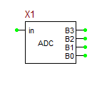
This is a 5-pin mixed-signal device with an analog input and 4 digital outputs. Based on the specified maximum input voltage level, a total of 16 discrete voltage levels are established. The block fits the input analog voltage between two of these 16 discrete levels and outputs the 4-bit binary equivalent to 4 digital pins B0-B3 representing the LSB and MSB, respectively.
Parameters:
| NAME | PARAMETER | UNITS | DEFAULT | NOTES |
|---|---|---|---|---|
| max_val | maximum input voltage | V | 5 |
4-Bit D/A Converter Block
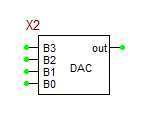
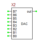
This is a 5-pin mixed-signal device with 4 digital inputs and an analog output. Based on the specified low and high output voltage levels, a total of 16 discrete voltage levels are established. The block converts the input 4-bit word (B0-B3 representing the LSB and MSB, respectively) to the corresponding discrete voltage level and outputs it as an analog voltage signal.
Parameters:
| NAME | PARAMETER | UNITS | DEFAULT | NOTES |
|---|---|---|---|---|
| out_low | output low voltage level | V | 0 | |
| out_high | output high voltage level | V | 5 |
4-Bit Signal Digitizer Block
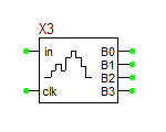
This is a 6-pin mixed-signal device with an analog input, a digital clock and 4 digital outputs. It samples its analog input signal at the period of the supplied digital clock. The digitized version of the input signal is sent out to 4 digital outputs B0-B3 representing the LSB and MSB, respectively.
Parameters:
| NAME | PARAMETER | UNITS | DEFAULT | NOTES |
|---|---|---|---|---|
| r_in | input resistance | Ω | 10G | |
| max_val | maximum input voltage | V | 5 |
8-Bit A/D Converter Block
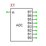
This is a 9-pin mixed-signal device with an analog input and 8 digital outputs. Based on the specified maximum input voltage level, a total of 256 discrete voltage levels are established. The block fits the input analog voltage between two of these 256 discrete levels and outputs the 8-bit binary equivalent to 8 digital pins B0-B7 representing the LSB and MSB, respectively.
Parameters:
| NAME | PARAMETER | UNITS | DEFAULT | NOTES |
|---|---|---|---|---|
| max_val | maximum input voltage | V | 5 |
8-Bit D/A Converter Block
This is a 9-pin mixed-signal device with 8 digital inputs and an analog output. Based on the specified low and high output voltage levels, a total of 256 discrete voltage levels are established. The block converts the input 8-bit word (B0-B7 representing the LSB and MSB, respectively) to the corresponding discrete voltage level and outputs it as an analog voltage signal.
Parameters:
| NAME | PARAMETER | UNITS | DEFAULT | NOTES |
|---|---|---|---|---|
| out_low | output low voltage level | V | 0 | |
| out_high | output high voltage level | V | 5 |
Clocked Sample-and-Hold Block
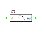
This device samples its input signal at a specified sampling period and holds the values of each sample during each clock cycle. The output signal is a quantized version of the input signal.
Parameters:
| NAME | PARAMETER | UNITS | DEFAULT | NOTES |
|---|---|---|---|---|
| T | sampling period | sec | 1 | required |
| duty_cycle | sampling pulse duty cycle | - | 0.1 | |
| Tmax | signal period or maximum duration | sec | 10 |
Digital Integrator Block
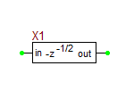
This device models a digital integrator with a Z-transform of -z-1/2, which is equivalent to a delay line with a delay of half the sampling period
Parameters:
| NAME | PARAMETER | UNITS | DEFAULT | NOTES |
|---|---|---|---|---|
| T | sampling period | sec | 1 | required |
Discrete Convolution Block
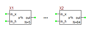
These blocks perform an N-point discrete convolution of their input signals. Both of the input signals x(t) and h(t) are sampled at the specified sampling period. The samples of x(t) are then shifted in time for the convolution. The output signal is a pulse train of the same period with the specified duty cycle. The input signal of these block can be either continuous-time signals or pulse trains of the specified period.
Parameters:
| NAME | PARAMETER | UNITS | DEFAULT | NOTES |
|---|---|---|---|---|
| T | sampling period | sec | 1 | required |
| rise_time | window rise time | sec | 0 | |
| fall_time | window fall time | sec | 0 | |
| duty_cycle | output pulse duty cycle | - | 0.1 | |
| gain | output gain | - | 1 |
Discrete Fourier Transform (DFT) Block
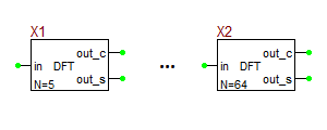
These blocks perform an M-point discrete Fourier transform (DFT) of their input signal and then sample each period of the Fourier transform N times in the frequency domain. The output signals are two finite sequence pulse trains representing the cosine and sine DFT transforms. The input signal of these block can be either a continuous-time signal or a pulse train of the specified period.
There are ten DFT blocks for M = 5, 6, 7, 8, 9, 10, 12, 16, 32, 64. In each case, the total duration of the transform window is MT, where T is the sampling period. By default, the frequency domain sampling starts at t = MT and takes place over one spectral period equal to fs = 1/T. You can change the sampling start time by "n_delay" temporal periods. n_delay = 0 by default, but it can be either positive or negative. You can also extend spectral sampling to more than one spectral period by increasing the value of the parameter "n_dur", which has a default value of 1.
Parameters:
| NAME | PARAMETER | UNITS | DEFAULT | NOTES |
|---|---|---|---|---|
| T | sampling period | sec | 1 | required |
| N | sequence length | - | 5 | required |
| rise_time | window rise time | sec | 0 | |
| fall_time | window fall time | sec | 0 | |
| duty_cycle | output pulse duty cycle | - | 0.1 | |
| n_delay | number of delayed period before sampling | - | 0 | |
| n_dur | number of frequency-sampled periods | - | 1 |
Discrete-Time Fourier Transform (DTFT) Block
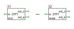
These blocks perform an N-point discrete-time Fourier transform (DTFT) of their input signal and output the transform as two temporal voltage signals representing the cosine and sine DTFT transforms. The The input signal of these block can be either a continuous-time signal or a pulse train of the specified period.
There are ten DTFT blocks for N = 5, 6, 7, 8, 9, 10, 12, 16, 32, 64. In each case, the total duration of the transform window is NT, where T is the sampling period.
Parameters:
| NAME | PARAMETER | UNITS | DEFAULT | NOTES |
|---|---|---|---|---|
| T | sampling period | sec | 1 | required |
| rise_time | window rise time | sec | 0 | |
| fall_time | window fall time | sec | 0 |
Discrete-Time Signal Hold Block
This device takes a pulse train of a specified period as its input and holds the value of each pulse's amplitude during each clock cycle at the output.
Parameters:
| NAME | PARAMETER | UNITS | DEFAULT | NOTES |
|---|---|---|---|---|
| T | sampling period | sec | 1 | required |
| duty_cycle | sampling pulse duty cycle | - | 0.1 | |
| rise_time | window rise time | sec | 0 | |
| fall_time | window fall time | sec | 0 | |
| Tmax | signal period or maximum duration | sec | 10 |
Finite Sequence Signal Sampler Block
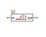
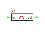
This device samples its input signal during a finite time window at a specified sampling period and outputs a pulse train of finite duration with a specified duty cycle.
Parameters:
| NAME | PARAMETER | UNITS | DEFAULT | NOTES |
|---|---|---|---|---|
| T | sampling period | sec | 1 | required |
| duty_cycle | sampling pulse duty cycle | - | 0.01 | |
| rise_time | window rise time | sec | 0 | |
| fall_time | window fall time | sec | 0 | |
| n | number of samples | - | 5 | |
| start | start time | sec | 0 |
Generalized Digital Filter Block
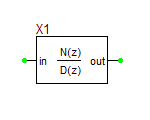
This block models a generalized digital filter characterized by a rational transfer functions in the Z-transform domain variable z:
[math] H(z) = \frac{N(z)}{D(z)} = \frac{ \sum_{m=0}^{M} b_m z^m }{ \sum_{n=0}^{N} a_n z^n } [/math]
subject to the requirement N ≥ M. To access the parameters of this block, you have to click the Edit Model... button of its property dialog.
Parameters:
| NAME | PARAMETER | UNITS | DEFAULT | NOTES |
|---|---|---|---|---|
| deg | highest degree of z in transfer function | - | 2 | required |
| coeff_den | denominator coefficients array: coefficients of powers of (-z1/2), highest power first | - | 1 0 1 0 1 | required |
| coeff_num | numerator coefficients array: coefficients of powers of (-z1/2), highest power first | - | 1 0 0 0 0 | required |
| freq | sampling frequency | Hz | 1 | required |
One-Shot Sample-and-Hold Block
This device follows its input signal and samples it at a specified instant of time. It holds the value of that sample at its output indefinitely.
Parameters:
| NAME | PARAMETER | UNITS | DEFAULT | NOTES |
|---|---|---|---|---|
| T | sampling period | sec | 1 | required |
| Tmax | signal period or maximum duration | sec | 10 |
Signal Sampler Block
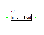
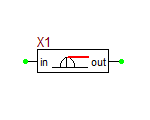
This device samples its input signal at a specified sampling period and outputs a pulse train with a specified duty cycle.
Parameters:
| NAME | PARAMETER | UNITS | DEFAULT | NOTES |
|---|---|---|---|---|
| T | sampling period | sec | 1 | required |
| duty_cycle | sampling pulse duty cycle | - | 0.01 | |
| rise_time | window rise time | sec | 0 | |
| fall_time | window fall time | sec | 0 |
Temporal Window Block
This device gates its input signals in time from instant t = T1 to instant t = T2.
Parameters:
| NAME | PARAMETER | UNITS | DEFAULT | NOTES |
|---|---|---|---|---|
| T1 | start time | sec | 0 | |
| T2 | stop time | sec | 1m | |
| rise_time | window rise time | sec | 0 | |
| fall_time | window fall time | sec | 0 |
