EM.Picasso Tutorial Lesson 2: Analyzing a CPW-Fed Folded Slot Antenna
Contents
Objective:
To construct a CPW-fed folded slot antenna in EM.Cube’s Planar Module, analyze it and visualize its near and far field characteristics and parameterize the design and explore its variations.
What You Will Learn:
In this tutorial lesson you will introduce slot (PMC) traces to your physical struture. You will also define coupled ports to model coplanar waveguide (CPW) structures.
Getting Started
Open the EM.Cube application and switch to Planar Module. Start a new project with the following attributes:
- Name: EMPicasso_Tutorial_4
- Length Units: mm
- Frequency Units: GHz
- Center Frequency: 1.7GHz
- Bandwidth: 0.6GHz
- Planar Mesh Density: 30 cells/λeff
- Number of Finite Substrate Layers: 1
- Layer Stack-up:
- Top Half-Space: Vacuum
- Middle Layer: ROGER RT/Duroid 5880, εr = 2.2, μr = 1, σ = σm = 0, thickness = 1.2mm
- Bottom Half-Space: Vacuum
Drawing the Slot Line Components
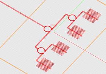
Create a PMC group on the Navigation Tree and call it PMC_1. Draw 13 rectangle strip objects with dimensions and locations given in the table at the top of next page. As you can see from the table, there are many identical objects, which you can copy and paste from one another and move them to their right locations.
|
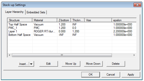
After you finish the drawing of all slot line components, open up the stack-up manager to examine the layer hierarchy of your planar structure. Your slot (PMC) trace must be sandwiched between the dielectric layer and the top half-space. If not, move the trace up. Also, make sure that the botton half-space is free space. Remember that the default settings of the bottom half-space is PEC when you create the project.
Defining Sources & Assigning Ports
You are going to define two coupled de-embedded sources for your two input slot lines, which together create a coplanar waveguide (CPW) feed line. A practical CPW transmission lines operates at the dominant odd mode. In the CPW odd mode, the electric fields across the two coupled slot lines are equal in magnitude, but they are 180o out of phase. Therefore, you are going to define two sources with a unit amplitude and a 180o phase difference.
Define a +Y-directed de-embedded source on the object Rect_Strip_12 (L12) and another +Y-directed de-embedded source on the object Rect_Strip_13 (L13). Set both offset values to zero. Both source should have an amplitude of 1V. The first source should have a zero phase while the second should have a phase of 180o.
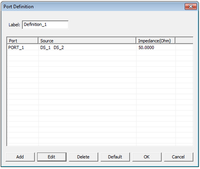
Next, you have to define an input port for your antenna. Open the Port Definition Dialog. The initial default setting shows two ports PORT_1 and PORT_2 assigned to the sources DS_1 and DS_2, respectively. In other words, the two ports are independent of each other. To define a single coupled port, first delete PORT_2 by selecting and highlighting in the port list and clicking the Delete button of the dialog. At this point, you have only PORT_1 defined. Select and highlight PORT_1 in the port list and click the Edit button of the dialog. This opens up Edit Port Dialog, which has two tables in the “Sources” section. The table on the left is called “Available Sources” and the one on the right is called “Associated Sources”. At this point, you should have DS_2 in the left table and DS_1 in the right table. Select DS_2 from the left table and click the Right Arrow (→) button of the dialog to transfer it to the right table.
Now, you have both sources DS_1 and DS_2 associated with PORT_1. Accept the change and close the dialog to return to the Port Definition Dialog. In the port list, you should now see both DS_1 and DS_2 next to PORT_1 (see the figure on the right).
| |
In EM.Cube’s Planar Module, you can a define a CPW transmission line using two parallel and identical rectangle strip slot (PMC) objects separated by the proper distance and exciting them with two sources of identical amplitudes but 180° phase difference. |
| |
De-embedded sources use Prony’s exponential approximation method to extract the scattering parameters. You can set the number of Prony’s modes in the source’s property dialog. This number is one by default, corresponding to a pair of incident and reflected dominant propagation modes. In CPW structures, besides the desired “odd” mode, you might excite the unwanted “even” mode, too. In such cases, you can set the number of Prony modes equal to 2 to obtain more accurate results. |
Running a Planar MoM Analysis
Before running a simulation, let’s take a look at the planar mesh of your slot antenna. The specified mesh density for this project is 30 cells/λeff. As you would expect, both feed lines with de-embedded ports on them are extended to 2λg. For slot lines,λeff = λ0/√εeff, where εeff ≈ (εr + 1)/2, if the medium above the slot is vacuum and the one beneath it is a dielectric of permittivity εr. Here you can see a planar mesh consisting solely of rectangular cells. EM.Cube’s “Hybrid Planar Mesher” identifies the junctions and joints among rectangular objects of the same width and generates a smooth rectangular transition mesh in those areas. This happens if you create all those joints objects (L2, L3, L6, L7, L10, L11). Otherwise, if you simply connect rectangular objects from their elongated sides without paying particular attention to microstrip discontinuities like bends and tee or cross junctions, a triangular mesh will be generated at these connection areas. Results like port or radiation characteristics are usually good and comparable in both cases. However, if you are interested in detailed current distribution plots, then you need to increase the mesh density adequately in the latter case.Run a quick planar MoM analysis of your folded slot antenna and visualize its current distribution and 3D radiation pattern. Keep in mind that since your slot trace is purely PMC, the electric surface current density is zero everywhere, and you should look at the magnetic current density plots instead. Note that magnetic current density has units of V/m, which is the same as that of electric field. The radiation pattern is typical of a dipole antenna as you would expect. The port characteristics are reported as:
S11: -0.016278 -0.076813j
S11(dB): -22.100521
Z11: 47.839321 -7.394976j
Y11: 0.020415 +0.003156j
Running a Frequency Sweep
Next, you will run a frequency sweep of your folded slot antenna to examine its frequency response and resonance behavior. Keep in mind that an adaptive frequency sweep does not generate current distribution plots or 3D radiation patterns at each frequency sample, but a uniform frequency sweep does. Therefore, first run a uniform frequency sweep with the following parameters:
- Start Frequency: 1.4GHz
- End Frequency: 2.0GHz
- Number of Frequency Samples: 13
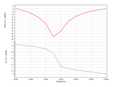
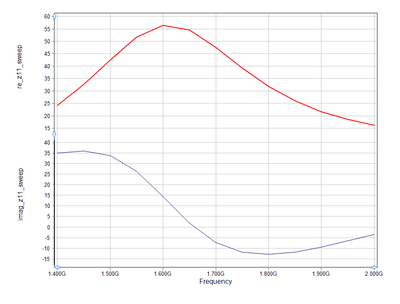
You will see that around 1.65GHz, the imaginary part of Z11 (i.e. input reactance) vanishes. Additionally, around the same frequency, the magnitude of S11 (return loss) dips into a deep minimum. This a good sign that your antenna both is both resonant and impedance-matched at that frequency.
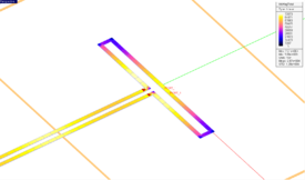
The figures below show the magnetic current distributions on the slot antenna and its CPW feed line at three different frequencies:
Next, run an adaptive frequency sweep with the following parameters:
- Start Frequency: 1.4GHz
- End Frequency: 2.0GHz
- Min No. of Frequency Samples: 5
- Max No. of Frequency Samples: 15
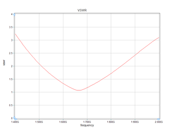
- Convergence Criterion: 0.02
At the end of the adaptive sweep, graph the data files “S11_RationalFit.CPX” and “Z11_RationalFit.CPX” in EM.Grid. From the S11 and Z11 graphs you can see that the actual resonant frequency is about 1.665GHz. You can also check the voltage standing wave ration of your antenna structure by graphing the file “VSWR_RationalFit.DAT”. In this graph, you can see the minimum VSWR value of 1.06. The two red horizontal lines mark VSWR = 1.0 and VSWR = 1.5.
