EM.Libera Tutorial Lesson 4: Analyzing Radar Cross Section of Surface and Solid Targets
Contents
- 1 Objective:
- 2 What You Will Learn:
- 3 Getting Started
- 4 Creating a Rectangular Plate Object
- 5 Source Definition
- 6 Defining Project Observables
- 7 Mesh Generation
- 8 Running the Surface MoM Simulation
- 9 Viewing the Simulation Results
- 10 Plane Wave Sources with Oblique Incidence
- 11 Creating a Hemispherical Metallic Hump
- 12 Adding a Hemispherical Dielectric Hump
- 13 Using a TE-Polarized Plane Wave Source
Objective:
To construct perfect electric conductor (PEC) and dielectric targets in EM.Cube’s MoM3D Module, illuminate them with plane wave sources and compute their radar cross section (RCS).
What You Will Learn:
In this tutorial lesson, first you will consider a rectangular metal plate and excite it with normally and obliquely incident plane wave sources. Then, you will create a hemispherical metallic hump on your flat plate. Finally, you will replace the metallic hump with a dielectric hump and see its effect on the RCS of the target. This tutorial will guide you through all necessary steps required to set up and perform a basic Surface MoM simulation and visualize and graph the simulation results.
Getting Started
Open the EM.Cube application and switch to MoM3D Module. Start a new project with the following attributes:
- Name: SMOMLesson1
- Length Units: mm
- Frequency Units: GHz
- Center Frequency: 1.0
- Bandwidth: 1.0
Creating a Rectangular Plate Object
Select the Rectangle Strip Tool from the Object Toolbar (or use the keyboard shortcut F2, or the menu Object → Surface → Rectangle Strip).

With the rectangle strip tool selected, click the origin (0,0,0), and drag the mouse to start drawing a rectangle. Observe the changing X and Y Dimension values in the dialog box as you drag the mouse back and forth. When both X and Y Dimensions reach a value of 1200 units, left-click to “lock-in” the value. You may also left-click at any point and adjust the length by typing in a value of 1200 in the object’s property dialog. Since you drew a very large plate, it may full up the entire screen. You can zoom to fit your structure into the screen using the keyboard shortcut Ctrl+E or by clicking the Zoom Extents ![]() button of View Toolbar.
button of View Toolbar.
Since the center frequency of the project is 1GHz, the operating wavelength is λ0 = 300mm. In this case, the electrical size of your metal plate is 2λ0 × 2λ0.
Source Definition
In order to analyze electromagnetic scattering from targets, you illuminate them with a plane wave source and compute the scattered (or reflected) fields. To define a plane wave source, right click on the Plane Waves item of the Sources section in the Navigation Tree and select Insert New Source… from the contextual menu. The Plane Wave Dialog opens up with a number of default settings. Your plane wave source will have an "Amplitude" of 1V/m and a zero "Phase". You will keep the default TMz polarization. In the “Incident Angle” section of the dialog you need to enter the elevation θ and azimuth φ angles in the standard spherical coordinate system. Accept the default values: θ = 180° andφ = 0°, which represent an X-polarized normally incident plane wave. Note that In EM.Cube, plane waves are characterized by their unit propagation vector. Therefore, for a downward-looking normally incident plane wave, θ = 180°, and for an upward looking wave (along the positive Z-axis), θ = 0°.
Defining Project Observables
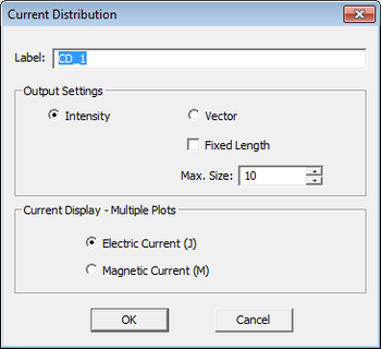
Project observables are output quantities that you would like to compute at the end of a SMOM simulation. By default, the Surface MoM solver does not generate any output data unless you define one or more project observables before you start a simulation. Current distribution observables are used to visualize the surface electric and magnetic currents on the metallic and dielectric structures. To define a current distribution observable, right click on the Current Distributions item in the “Observables” section of the Navigation Tree and select Insert New Observable… This opens up the Current Distribution Dialog. Keep all the default options and close the dialog. A new entry CD_1 is added to the Navigation Tree.
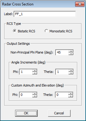
Next, you will define a Radar Cross Section (RCS) observable. This is one of the two far fields observable types. Right-click on the Far Fields item in the Navigation Tree and select Insert New RCS... from the contextual menu. The Radar Cross Section Dialog opens up. In the "RCS Type" section of the dialog, select the default "Bistatic RCS" option. Change the values of "Angle Increment" for both Theta and Phi from the default value of 5° to 1°, and close the dialog. This will set a very high angular resolution for both elevation and azimuth spherical observation angles.
Mesh Generation
EM.Cube has several types of mesh generators that are used to discretize the physical structure for the numerical solution of Maxwell's equations either directly or in their asymptotic forms. The Surface MoM simulator of EM.Cube's MoM3D Module uses a triangular surface mesh generator that creates a set of triangular cells on surface objects or on the surface of solid objects. The triangular cells are usually generated to be as regular as possible with almost the same surface area throughout the entire mesh. The Surface MoM solver ignores all the lines or curve objects.
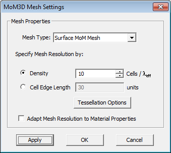
You can control the mesh resolution in two ways. The first method is to set the "Mesh Density" in the form of the number of cells per wavelength. In this case, your mesh will be frequency dependent, and the number of cells on a rectangular object of fixed dimensions will increase as the frequency increases. For example, the default mesh density is 10 cells per wavelength. This means that on a rectangular plate of dimensions λ0 × λ0, you will have exactly 100 square cells but slightly more than 200 regular triangular cells. With the same mesh density, your 2λ0 × 2λ0 metal plate will have 400 square cells and 934 regular triangular cells. The second method of controlling the mesh is by setting a fixed "Edge Length" for the mesh cells. The edge length is set in the project units. A mesh of this kind will be frequency-independent.
The mesh properties can be accessed by clicking the Mesh Settings ![]() button of the Simulate Toolbar (or using the keyboard shortcut Ctrl+G or via the menu Simulate → Discretization → Mesh Settings). To view the mesh, click the Show/Generate Mesh
button of the Simulate Toolbar (or using the keyboard shortcut Ctrl+G or via the menu Simulate → Discretization → Mesh Settings). To view the mesh, click the Show/Generate Mesh ![]() button of the Simulate Toolbar (or alternatively use the keyboard shortcut Ctrl+M). In general, the mesh view shows how the simulation engine sees your physical structure. To exit the mesh view mode, use the keyboard's "Esc" key or click the Show Mesh button of the Simulate Toolbar one more time.
button of the Simulate Toolbar (or alternatively use the keyboard shortcut Ctrl+M). In general, the mesh view shows how the simulation engine sees your physical structure. To exit the mesh view mode, use the keyboard's "Esc" key or click the Show Mesh button of the Simulate Toolbar one more time.
Running the Surface MoM Simulation
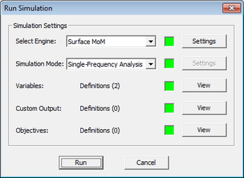
At this time, your project is ready for the Surface MoM simulation of your metal plate structure. Click the Run ![]() Button of the Simulate Toolbar to open up the Simulation Run Dialog. Or alternatively, use the keyboard shortcut Ctrl+R, or the menu Simulate → Run… By default, when you open the Run Dialog in EM.Cube's MoM3D Module, the Wire MoM solver is shown as the default simulation engine. From the "Select Engine" drop-down list, select the "Surface MoM" option. The simplest simulation mode in EM.Cube is “Analysis”. In this mode, your physical structure is taken “As Is” and its mesh is passed to the Surface MoM simulation engine, along with the necessary information regarding the sources and observables. Since Surface MoM simulations are frequency-domain, you will run a "Single-Frequency Analysis". Select this option from the drop-down list labeled "Simulation Mode".
Button of the Simulate Toolbar to open up the Simulation Run Dialog. Or alternatively, use the keyboard shortcut Ctrl+R, or the menu Simulate → Run… By default, when you open the Run Dialog in EM.Cube's MoM3D Module, the Wire MoM solver is shown as the default simulation engine. From the "Select Engine" drop-down list, select the "Surface MoM" option. The simplest simulation mode in EM.Cube is “Analysis”. In this mode, your physical structure is taken “As Is” and its mesh is passed to the Surface MoM simulation engine, along with the necessary information regarding the sources and observables. Since Surface MoM simulations are frequency-domain, you will run a "Single-Frequency Analysis". Select this option from the drop-down list labeled "Simulation Mode".
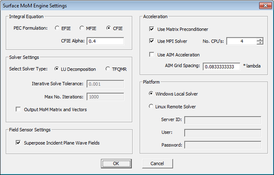
Before starting the simulation, let us take a look at some simulation parameters and options. Click on the Settings button next to the "Select Engine" drop-down list to open the Surface MoM Engine Settings Dialog. This dialog contains a number of solver options. For problems that involve linear system smaller than N = 5000, it is recommended to use the "LU Decomposition" solver, while for large linear systems, the iterative TFQMR solver is the more efficient choice. For this project, chose the "LU" option. Also check the option "Use Matrix Preconditioner". Chances are your computer has a multicore CPU. Check the option "Use MPI Solver" and set the number of CPUs to 4 or higher depending on the number of cores of your CPU.
| |
EM.Cube's Surface MoM solver is highly parallelized for multicore CPU architectures. Surface MoM simulations can greatly speed up if you choose the MPI solver. |
To run the simulation, click the Run button of the Simulation Run Dialog. A separate window pops up displaying messages from the simulation engine. Once the simulation is completed, the Navigation Tree is populated with simulation results, most notably under Current Distributions and Far Fields nodes.
Viewing the Simulation Results
EM.Cube’s computational modules usually generate two types of data: 2D and 3D. Examples of 2D data are Cartesian and polar radiation patterns. 2D data are graphed in EM.Grid. Examples of 3D data are near field distributions and 3D radiation patterns. 3D data are visualized in EM.Cube’s project workspace and the plots are usually overlaid on the physical structure.
First, you will visualize the current distribution on the metal plate. The "Current Distribution" section of the Navigation Tree plots both electric currents (J) and magnetic currents (M). Each current distribution observable contains a list of twelve amplitude and phase plots for all the six current components: Jx, Jy, Jz, and Mx, My, Mz. There are also two additional plots for the magnitude of total electric current and total magnetic current. In the case of your project, since you have only a PEC surface, M = 0. Click on any of these plots to display them in the project workspace. You can use the standard view operations such as dynamic zoom, rotate view, pan view, etc. to better examine these plots. As you can see from the figure below, the current distribution on the metal plate is concentrated at the edges of the plate and is relatively uniform elsewhere.
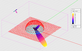
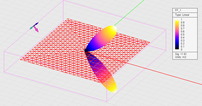
The Far Fields section of the Navigation Tree contains three different 3D RCS pattern plots: the Theta component of the RCS, the Phi component of the RCS, and the Total RCS. You will notice that the RCS plots are all centered at the origin of coordinates. This is due to the fact that the scattering patterns are calculated in a standard spherical coordinate system centered at (0, 0 , 0).
Note that in the figure below for the 3D RCS pattern, the metal plate has been replaced with a simple wireframe. You can turn objects into a simple wireframe in the project workspace by right-clicking on their surface and selecting "Freeze" from the contextual menu. In the freeze state you cannot select objects or highlight them in the project workspace. You can, however, select a frozen object from the Navigation Tree. To restore a frozen object to its normal display, you have to right-click on its name in the Navigation Tree and remove the check mark before "Freeze" from the contextual menu.
Besides 3D visualization of the RCS, you can plot 2D RCS graphs at certain plane cuts. A list of all the 2D output data files generated at the end of a simulation can be viewed in EM.Cube’s Data Manager. To open this dialog, click the Data Manager ![]() button of Simulate Toolbar, or use the keyboard shortcut Ctrl+D, or access the menu Simulate → Data Manager, or right click on the Data Manager item in the “Observables” section of the Navigation Tree and select Open Data Manager…
button of Simulate Toolbar, or use the keyboard shortcut Ctrl+D, or access the menu Simulate → Data Manager, or right click on the Data Manager item in the “Observables” section of the Navigation Tree and select Open Data Manager…
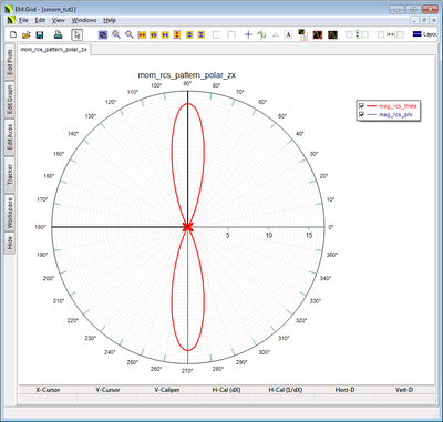
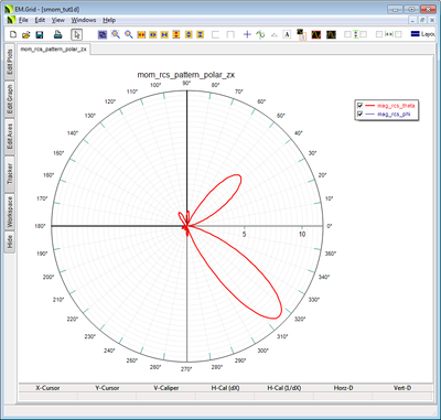
The 2D RCS patterns can be plotted as both Cartesian and polar graphs. Open up the Data Manager dialog and spot Cartesian pattern data files with a “.DAT” file extension as well as the polar (angular) data files with a “.ANG” file extension. The figure below shows the Cartesian and polar RCS plots in the ZX plane cut. Besides the three principal XY, YZ and ZX plane cuts, there are also data files for one additional user defined Phi‐plane cut, which by default is calculated at φ = 45o.
Plane Wave Sources with Oblique Incidence
In the previous section, your plane wave source was normally incident with θ = 180° and φ = 0°. In addition, it had a "TMz" polarization with an X-directed electric field. The propagation vector and electric and magnetic field polarization vectors are shown as a trident at the top of the pink plane wave box that encloses your structure in the project workspace. If you change the polarization of a normally incident plane wave source to "TEz", its electric field polarization vector will rotate by 90° clock wise and will become -Y-directed.
You can define a plane wave source with an arbitrary polarization and an arbitrary propagation vector. However, in most practical cases, you will use a normally or obliquely incident, TMz or TEz polarized, plane wave with arbitrary incident angles "Theta" and "Phi". In this section of the tutorial lesson, you will define a TMz-polarized plane wave illuminating from the left side of the metal plate at an angle of 45° with respect to the zenith. This translates to θ = 135° and φ = 0°. Open the property dialog of your plane wave source from the previous part and change the values of Theta and Phi accordingly. Run a new Surface MoM analysis of your structure and view the simulation results.
As you can see from the above plots, with a TM-polarized obliquely incident plane wave source, the peaks of the currents at the edges have shifted forward towards the front corners of the metal plate. The RCS plot shows two very strong scattered lobes along the θ = 45° and θ = 135°. These correspond to the so-called reflected and transmitted rays had the metal plate been a infinitely large horizontal PEC plane.
Creating a Hemispherical Metallic Hump
In this part of the tutorial lesson, you will build a hemispherical metallic hump and place it at the center of your rectangular metal plate. To do so, first you will use the Object Toolbar's "Sphere Tool" (keyboard shortcut: F6) to draw a sphere of radius 150mm. Center the sphere at (0, 0 , 0). EM.Cube allows you to draw incomplete spheres with start and end angles different than 0° and 360°, respectively. For a hemisphere, set the start and end angles to 0° and 180°, respectively, in the sphere's property dialog.
The Surface MoM mesh generator automatically conjoins all the objects that belong to the same material group. This is equivalent to a "Boolean Union" operation. A consistent surface triangular mesh of the resulting union object is then generated. When your objects are connected through a shared common surface, a special connection mesh region is created to ensure mesh continuity between the two overlapping objects. This connection mesh region is displayed in a different color (aqua or light blue in this case).
Run a new Surface MoM simulation of the metal plate structure with a hemispherical metallic hump at its center and visualize the results. From the RCS pattern plot, you can see that the reflected lobe has almost disappeared due to the hump.
Adding a Hemispherical Dielectric Hump
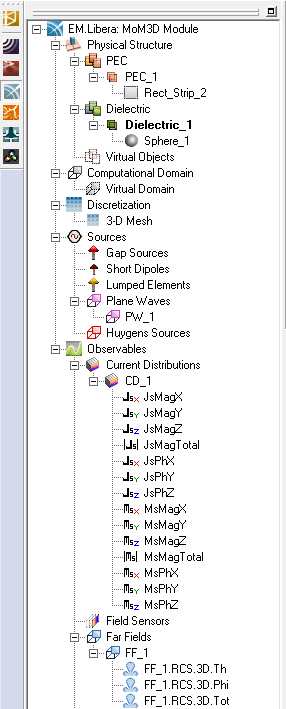
In this part of the tutorial lesson, you will see the effect of replacing the metallic hump with a dielectric hump of the same geometry and dimensions. EM.Cube's MoM3D Module categorizes and organizes the CAD objects based on their material composition. Currently there are two material types: Perfect Electric Conductor (PEC) and Dielectric. When you drew your first rectangle object in the beginning, its was assumed to be a PEC by default. A new node called PEC_1 was created and inserted to the "Physical Structure" section of the Navigation Tree. When you draw your sphere object, it was simply added to the same PEC_1 group. This means that both the rectangle object Rect_Strip_1 and the spherical object Sphere_1 are of the perfect electric conductor type with the same red color.
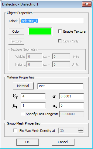
Next, you will create a dielectric material group to accommodate your dielectric hump. Right-click on the Dielectric item in the Physical Structure section of the Navigation Tree and select Insert New Dielectric... from the contextual menu. The New Dielectric Dialog opens up. Besides a name and a color, dielectric objects have other properties like the permittivity εr and conductivity σ. You can enter these values manually or you can use EM.Cube's material list. Click on the Meterial button of the dialog to open EM.Cube's Material List dialog. You can type any letter on your keyboard and more the selection to the first material starting with that letter. Select "PVC" with εr = 4, and close the dialogs to return to the project workspace.
When you create a new material group, it becomes the active group in the Navigation Tree. This means that all the new objects your draw in the project workspace will belong to this active group. You can change the active group to any group in the Navigation Tree by right-clicking on the group's name and selecting Activate from the contextual menu. With the new Dielectric_1 group active, you can start drawing a new sphere similar to the one you drew in the previous part. However, you have to delete the metallic sphere first to open the space for the new one. Alternatively, you can move objects between different material groups. Instead of deleting the old red metallic hemisphere and drawing a new green one under the Dielectric_1 group, you can simply move the old red metallic hemisphere object to the Dielectric_1 group. to do so, select Sphere_1 either in the project workspace or on the Navigation Tree and select Move To from the contextual menu. This leads further to two submenu options: PEC_1 and Dielectric_1. Select the latter and Sphere_1 will move under Dielectric_1. You will notice the color of the hemispherical hump now turns into bright green. Check out the mesh of the new structure. You can see the connection mesh regions at the boundary between the two different material types.
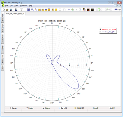
Run a new Surface MoM simulation of this structure and visualize the results. From the RCS pattern plot, you can see that the reflected lobe has come back again due to the presence of the penetrable dielectric hump.
Using a TE-Polarized Plane Wave Source
Next, you will change the polarization of the plane wave source to TEz with the same incident angles. You do this in the "Polarization" section of the plane wave source's property dialog. Run a new Surface MoM analysis and view the simulation results again. This time, with a TE-polarized obliquely incident plane wave source, you can see that the reflected lobe has decreases again, but has sizable back-scattered lobe has emerged.
