EM.Ferma Tutorial Lesson 9: Exploring Coplanar Waveguide Transmission Lines
Contents
What You Will Learn
In this tutorial you will construct and analyze more complicated types of multi-conductor transmission lines such as various coplanar waveguide structures with and without a dielectric substrate or conductor backing.
A coplanar waveguide (CPW) transmission line consists of a center metallic strip located between two wide grounded metallic strips on the two sides. All the three strips are collocated on the same plane. The width of the center strip (also called center conductor) is denoted by s. The gap between the center strip and the lateral ground strips on either side is denoted by w and is known as the slot width. In practice, a dielectric substrate is used to support the three metallic strips. The dielectric substrate can be an infinite half-space or a layer of finite thickness. The simplest CPW utilizes an air substrate. This can be realized using a very thin membrane and does have practical applications. The dielectric substrate may also have a PEC ground backing on its other side.
Getting Started
Open the EM.Cube application and switch to EM.Ferma. Start a new project with the following attributes:
Constructing the Basic CPW Line
Create two PEC groups PEC_1 and PEC_2 in the Navigation Tree and draw the following three rectangle strip objects:
| Object | Group | LCS Coordinates | Dimensions |
|---|---|---|---|
| Rect_Strip_1 | PEC_1 | (0, 0, 0) | 25mm × 1mm |
| Rect_Strip_2 | PEC_2 | (0, 6.5mm, 0) | 25mm × 10mm |
| Rect_Strip_3 | PEC_2 | (0, -6.5mm, 0) | 25mm × 10mm |
Open the Domain Settings dialog and change the offset values in the various directions according to the following table:
| Offset | Value |
|---|---|
| -X | 10mm |
| +X | 10mm |
| -Y | 0mm |
| +Y | 0mm |
| -Z | 10mm |
| +Z | 10mm |
Also, define a 1V voltage source called VS_1 and associate it with the PEC_1 group, which contains the center conductor. Define a vertical X-directed field sensor observable called Sensor_1 and place it at (0, 0, 0). Note that the 2D quasi-static analysis will be performed on this sensor plane. The CPW structure has 10mm of clearance from the top and bottom domain boundary walls. However, the ground strips Rect_Strip_2 and Rect_Strip_3 touch the side boundary walls and are therefore held at zero potential.
Next, open the 2D Domain Settings dialog from the 2D Solution Planes item in the Navigation Tree and instruct EM.Cube to run a 2D quasi-static analysis of your CPW structure in the Sensor_1 plane. Designate VS_1 as the signal source.
Running a Quasi-Static Simulation of the Basic CPW Line
Your 2D solution domain has dimensions of 23mm × 20mm along the Y and Z directions, respectively. In order to have adequate mesh resolution on the center conductor and across the slot gaps, you will choose a cell size of 0.05mm along the Y direction. This will put 20 cells on the center conductor and across each slot gap. To have square mesh cells of dimensions 0.05mm × 0.05mm, you need to set the number of mesh cells equal to 460 and 400 along the Y and Z directions, respectively. Open the Mesh Settings dialog and make these changes. Keep in mind that the number of cell along the X direction does not matter because you will run a 2D analysis only on the YZ plane.
Run a quasi-static "Analysis" of your 2D CPW transmission line structure. At the end of the simulation, the output message window reports the computed values of the characteristic impedance and effective permittivity of the transmission line:
Z0: 143.148 Ohms
Epsilon_Effective: 1
An effective permittivity of one is expected as your structure represents an air-filled homogenous multi-conductor transmission line supporting a dominant TEM propagating mode. RF.Spice's CPW Line calculator predicts a characteristic impedance value of Z0 = 147.35Ω for this transmission line.
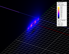
You can also view the electric field and electric potential results. The figure below in the middle shows the vector plot of the total electric field in the YZ plane. As you can see from the figure, the field is highly concentrated at the edges of the center conductor and in the gap regions between the center conductor and the two side ground strips.
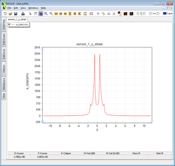
Open the Data Manager and plot the data files "Sensor_1_Y_ETotal.DAT" and "Sensor_1_Z_ETotal.DAT" in EM.Grid as shown in the figures below. The spikes in the figure on the left represent the field singularities at the edges of the metallic strips. On the other hand, the null at the center of the figure on the right (at Z = 0) corresponds to the zero field at the center of the center conductor.
Analyzing a CPW Line with a Dielectric Substrate
In this part of the tutorial lesson, you will add a finite-sized dielectric substrate underneath your CPW structure and will see its effect on the line characteristics. For this purpose, define a new dielectric material group called Dielectric_1 in the Navigation Tree. Assign Rogers RO4003C as the material from EM.Cube's Materials List. With the Dielectric_1 group active, draw a box object of dimensions 25mm × 23mm × 1.5mm and place its local coordinate system at (0, 0, -1.5mm). In other words, you will add a dielectric substrate of thickness 1.5mm and εr = 3.38 just underneath the CPW structure of the previous part.
Keep all the other settings the same as in the previous part. Adding the dielectric layer increases the total domain size along the Z-axis to 21.5mm. To maintain a square mesh cell size of 0.05mm, you have to set the number of cells to 460 and 430 along the Y and Z directions, respectively. Run an quasi-static "Analysis" of your 2D CPW line with the dielectric substrate. At the end of the simulation, the output message window reports the computed values of the characteristic impedance and effective permittivity of the transmission line:
Z0: 99.9166 Ohms
Epsilon_Effective: 2.05568
RF.Spice's CPW Line calculator predicts a characteristic impedance value of Z0 = 103.13Ω and an effective permittivity value of εeff = 2.04 for this transmission line. Note that since the dielectric substrate is fairly thick compared to the strip and slot width, it resembles a dielectric half-space underneath the CPW line. For this type of CPW line, there is an analytical formula for the effective permittivity, which is given by:
[math] \epsilon_{eff} = \frac{\epsilon_r + 1}{2} = \frac{3.38+1}{2} = 2.19 [/math]
Visualize the electric field and electric potential distribution plots as shown in the figures below. The field distribution is quite similar to the case of air substrate.
Plot the data files "Sensor_1_Y_ETotal.DAT" and "Sensor_1_Z_ETotal.DAT" in EM.Grid. Note the visible asymmetry of the graph below on the right. At Z = -1.5mm, there is a field discontinuity at the interface between air and the dielectric layer.
Adding Conductor Backing to a Thin Dielectric Substrate
In many practical RF circuits, the CPW lines are printed on thin conductor-backed substrates. To explore this type of conductor-backed CPW lines, open the property dialog of the dielectric substrate object (Box_1) and decrease its height by a half to 0.75mm. To make the substrate conductor-backed, open the Domain Settings dialog and set the "-Z Offset" equal to zero. This brings the bottom PEC domain boundary wall up and places it right underneath the substrate layer. The total domain size along the Z-axis is now reduced to 10.75mm. Accordingly, open the Mesh Settings dialog and change the number of cells along the Y and Z directions to 460 and 215, respectively.
Run an quasi-static "Analysis" of your 2D CPW line with the conductor-backed dielectric substrate. At the end of the simulation, the output message window reports the computed values of the characteristic impedance and effective permittivity of the transmission line:
Z0: 62.0829 Ohms
Epsilon_Effective: 2.60676
RF.Spice's CPW Line calculator predicts a characteristic impedance value of Z0 = 67.93Ω and an effective permittivity value of εeff = 2.51 for this transmission line.
Visualize the electric field and electric potential distribution plots as shown in the figures below. You can see from the figures that there is substantial field concentration between the center conductor and the underlying ground plane. In effect, the field of the conductor-backed CPW line looks more like a microstrip line as you saw earlier in Tutorial Lesson 4.
Plot the data files "Sensor_1_Y_ETotal.DAT" and "Sensor_1_Z_ETotal.DAT" in EM.Grid. In this case, the field below Z = -0.75mm (underneath the ground plane) is zero. However, at Z = -0.75mm, the vertical electric field has a nonzero value and it undergoes another discontinuity at Z = 0, which represents the interface between air and the top surface of the dielectric substrate.
![]() Back to EM.Ferma Tutorial Gateway
Back to EM.Ferma Tutorial Gateway


