Working with Symbol Editor
RF.Spice's Symbol Editor can be invoked from both the Workshop and the Device Manager. You use the Symbol Editor to edit and save symbols. Please note that there are slight differences in the appearance and functionality of the Symbol Editor depending on whether you open it from the Device Manager or from the Schematic Editor. Using the Symbol Editor in the Device Manager, you can create new symbols from the ground up. You can also modify all the symbols in the parts database. However, from the Workshop you can only edit the symbols of the parts in your currently open project. You can choose to save the modified symbol(s) to the current circuit project only. Or you can save your changes to your parts database and make them permanent.
What is a Symbol?
A symbol is a graphical object that RF.Spice A/D uses to represent a part or device. Every device in the Parts Database has an associated symbols. Some devices may have more than one associated symbol. When you place a part in your schematic, its symbol is drawn in the schematic window. You can move a part in your circuit by selecting and dragging its symbol around. A symbol is typically made up of a drawing, one or more texts and one or more pins. The drawing can be as simple as a box or a circle or very sophisticated graphics. The Symbol Editor provides a number of drawing tools: Line, Rectangle, Ellipse, Polygon and Arc. A symbol may contain a composite drawing involving several distinct shapes. The symbol's text(s) may include the device name and a number of parameter values.
What is a Pin?
Pins are used to connect a device to wires and other parts in your schematic. A symbol must have at least one pin to make the device connectable and useful. In the Symbol Editor, pins are displayed as very small hollow squares that are connected to the body of the device (graphics) using straight lines or leads. In the Schematic Editor, the pins of a part are displayed as small solid green circles. When you click on a pin in the Schematic Editor, its border turns red to imply that it has been selected. When you draw a wire in the Schematic Editor and drag it onto a pin, the pin's boundary turns to a red square, implying that a circuit connection to that pin is about to be made. Each pin of a symbol must have a unique name. You can use numbers or letters or a combination of them or longer meaningful names to identify the pins of a symbol.
Creating a New Symbol
To create a new symbol, first you have to open the Device Editor. Go to the File Menu of the Device Editor and select "New Symbol...". This opens up the Symbol Editor in a separate window. Symbol Editor has a default grid. The grid is used as a visual aid to draw graphics. The objects you draw in the Device Editor's Symbol Editor do not snap to the grid points. Pins, on the other hand, always snap to the grid points.
The following steps describe how to create a new basic symbol:
- Use one or more of the drawing tools, Line, Rectangle, Ellipse, Polygon and Arc, to draw your symbol.
- Using the "Pin Tool" define and place one or more pins. Name them properly. Use the "Line Tool" to connect the pins to the body of your device.
- Use the "Text Tool" to create a title for your symbol. For this purpose, draw a text box and place the text "[title]" in it.
- You may also want to place a text next to each pin to identify it. This can be the pin name or characters like "+" or "-".
- Save your symbol and give it a name to be stored in the Parts Database.
Drawing Objects
The simplest geometrical object is a line. Select the "Line Tool". Draw a line by holding down the left mouse button and dragging. Release the mouse button where you want to end the line. Note that when you select the Line Tool, the Symbol Editor enters the Line mode and will stay in that mode until you change its mode. This means that once you finish drawing your line object, you can continue drawing new line objects. The Symbol Editor's default or normal mode is the "Select Mode". Click the "Select Tool" (white arrow) button on the toolbar to enter the Select Mode.
To draw a rectangle or ellipse, select the respective tool from the toolbar and click on the first corner point. Hold down the left mouse button and drag it in the right direction until to get the right size for your new object. In the case of an ellipse, the first corner point indeed corresponds to the bounding box of the ellipse. You can use the "Polygon Tool" to draw a closed polygon. You start a polygon just like a line. Every time you click the left mouse button you can change the direction of your polygon and add a new side. Single-click on the right mouse (or double-click with the left) to finish your polygon. You don't have to connect back to the original point. The polygon will automatically closes upon completion. To draw an arc, select the "Arc Tool" and first draw a full ellipse. Once your full ellipse is completed, a new varying radial line pops out of the center of the ellipse, whose ends follows the current location of your mouse. This allows you to set the start point of your arc. Click at the desired start point and drag the mouse either clockwise or counter-clockwise to stretch the arc. Then, click at the desired end point to finish your new arc object.
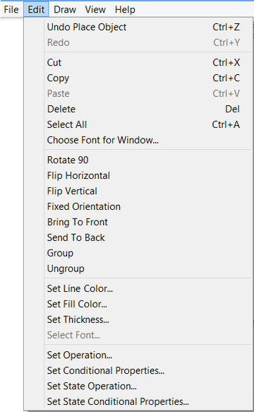
You can change the color of your lines and the boundaries of your objects from the default black. To do so, select one or more objects. Then select "Set Line Color..." from Symbol Editor's Edit Menu. This opens the color palette, where you can choose any desired color for your selected objects. You can set the thickness of the lines and object borders. By default, the line thickness is one point. To change an object's line thickness, first select the object and then select "Set Thickness..." from Symbol Editor's Edit Menu. Enter the desired value for the line thickness in the Thickness dialog. You can fill in rectangle, ellipse and polygon objects with any color. To fill in a object, first select it and then select "Set Fill Color..." from Symbol Editor's Edit Menu. This opens the same color palette, where you can choose your fill color. Symbol Editor's Edit Menu gives you more options to change or tailor your drawing. Some of these additional tools include rotating objects by 90 degrees, flipping horizontally or vertically, bringing objects to "Front" or sending them "Back" or grouping and ungrouping objects.
Adding Text
You can add text to a symbol for various purposes. A descriptive text such as the device type can be useful. To add text to your symbol, select the "Text Tool" from the toolbar and draw a text box of proper size at the desired location on the screen. The text dialog opens up immediately where you can type in your text.
You can also add a title to your symbol. Keep in mind that you might have several instances of the same device in your schematic. These parts of the same device type are identified on your schematic by their "Part Titles". You can make your symbol display the part title on the schematic. For this purpose, create a text box using the Text Tool and enter "[title]" for the text. The brackets indicate that the contents of the text box must be retrieved from the part's properties, in this case, its title. When you use this symbol in the Workshop, the title field will be replaced with the name of the part instance.
Besides its title, a part may have many other properties or parameters. You can also display the values of these parameters on the part's symbol. For example, a resistor has the parameter "resistance" with the units of Ohm. In order to display a part's parameter as part of the symbol, create a text box using the Text Tool and for its text enter the name of the device parameter enclosed by brackets. For example, enter "R = [resistance]" for your resistor. The [resistance] portion of the text field will be replaced with the value of resistance for that model. On the schematic, it will appear as "R = 1k" if the resistance value is 1k.
You can change the font of your symbol's text. Note that fonts are stored in the parts database, but the colors are not. To change the font, first select and highlight the text and then select "Set Custom Font..." from Symbol Editor's Edit Menu. Choose the desired font, font style, font size and click OK.
Editing an Existing Symbol from Device Editor
Symbols can be edited from both the Workshop and Device Editor. To edit an existing symbol from the Device Editor, go to the Edit Menu, and select "Edit Symbol...". This will open up the Select Symbol dialog. On the left you see a list of all the existing symbols in the Parts Database. Select the symbol you wish to edit and press the "Edit" button. You can also search for a symbol's name or use the search filters to quickly find your desired symbol.
Once you open a symbol for editing, you can add, delete, move and modify its constituent objects. To delete any object, select it and press the Delete Key. To move an object, select it and drag the object to the new location. When you hover the mouse over an object that can be moved, the cursor changes its shape from the Select Mode's default white arrow to small crossed double-arrows. Only lines, rectangles, ellipses and text boxes can be resized. To resize an object, first select it and then move the cursor to the corners or ends of the object. The cursor shape changes to an arrow with a plus sign for lines or a double-arrow for boxes and ellipses. Click and drag to resize the object. For rectangles, you can also resize from the center of sides. Pins and text fields can be edited by double clicking on them, whereby you can change the text or the pin name. Keep in mind that changes saved in the Device Editor are global.
Editing a Part's Symbol from Workshop
To edit a part's symbol from the Workshop, right click on the part's symbol in the schematic and select "Edit Symbol..." from the contextual menu. Or select the part first and then select "Symbol Operations > Edit Symbol..." from Schematic Editor's Edit Menu. Either way, the Symbol Editor opens up in a new window. As mentioned earlier, the appearance of the Symbol Editor in the Workshop is slightly different than the one in the Device Editor. The Workshop's Symbol Editor has a vertical toolbar on the left side that contains all the drawing tools. It also has a horizontal toolbar at the top which contains many additional buttons for graphical operations like group/ungroup, set line and fill colors, etc. Aside from the interface appearance, the functionality of the Workshop's Symbol Editor is mostly the same as the Device Editor's.
In the Workshop, you have to decide whether to save your changes locally or globally. In Symbol Editor's File Menu, you will find three items: "Store to Part Instance in Circuit", "Store to All Parts Using This Symbol in Circuit", and "Store to Database". The first option stores the modified symbol into the current project file only for the edited part, while the second option saves and updates the modified symbol for all the parts of the same type or even other parts in your current circuit project that share the same symbol just modified. The third option will also save and store the modified symbol into the Parts Database and make the change permanent for this project and all other projects in the future that will use the same symbol. However, keep in mind that the database changes are not retroactive and do not affect previously saved projects.
Setting Conditional Properties and Digital Operations
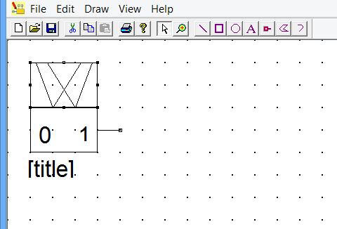
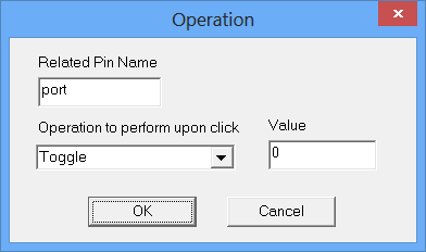
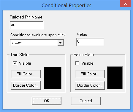
The Device Editor has the ability to create interactive symbols with conditional graphics â graphics that react to mouse clicks and pin states. This is most useful in digital simulations where some inputs such as buttons will change appearance with each click. For instance, if you edit the toggle switch's symbol (symbol name âtoggleâ), you will see that it is actually made of several conditional graphics. The changing part of the symbol indeed consists of three objects: an enclosing rectangle, a left-leaning polygon and a right-leaning polygon. The figure below shows the "Set Operation Dialog" and "set Conditional Properties Dialog". The "Related Pin Name" points to the pin whose condition is being tested to change the state of the graphics. In this case, if the pin âportâ is high, the right-leaning switch is visible; otherwise, it is invisible. As for the left-leaning switch, the graphic is visible only if the pin state is low, and it is invisible otherwise. The large rectangle overlaying the two switch graphics is the area where a mouse click will be detected and affect the pin value.
The "Set Operation Dialog" for the toggle switch defines the type of operation. Every time a click is detected inside the active area, the pin âportâ is toggled from high to low or vice versa. Therefore, in the drop-down list labeled "Operation to perform upon click", the "Toggle" option has been selected. Other options include Increment, Decrement, Set High, Set Low, Set Unknown, and Set Value To, with an edit box to enter the value. To make the rectangular active-click region an invisible graphic, go to the "Set Conditional Properties Dialog" of the rectangle object, where you will see both âVisibleâ checkboxes unchecked. The âCondition to evaluate upon clickâ should be set to some option other than âNo Conditionâ. The "Set Operation Dialog" for the left-leaning and right-leaning polygons is similar to that of the active-area rectangle object. Both have the "Toggle" option selected for the operation to perform upon click. However, in the "Set Conditional Properties Dialog" of the left-leaning polygon, you see the "Is Low" option selected for the condition to evaluate upon click. Also, the checkbox labeled "Visible" in the "True State" section is checked. On the other hand, in the "Set Conditional Properties Dialog" of the right-leaning polygon, you see the "Is High" option selected for the condition to evaluate upon click. In this case, too, the checkbox labeled "Visible" in the "True State" section is checked. During a digital simulation, the pin value is evaluated by the conditional properties discussed above, and the graphics changes accordingly.
Viewing and Setting Pin Names
To view a list of a symbol's pin names go to Symbol Editor's View Menu and select "View Pin List..." to open a dialog that displays the list of pin names. You may also view each individual pin name by selecting the Pin Tool and clicking on the pin itself. The Pin Name dialog displays the name of the selected pin, where you may change it. When creating a new device, its symbol's pin names must match the pin names of the device's simulation model. The pin names of the simulation model can be modified to match the names of the symbol pins in the Device Editor. However, if the symbol's pins are named correctly ahead of time, then this will save you a step. Most built-in simulation models have easy-to-remember pin names, such as R+ and R- for the pins of the resistor. If you don't know the simulation model's pin names, then use meaningful names for the symbol pins. Some examples of symbols that already have set pin names are:
List of Standard Device Symbols & Their Pins
Â
